DSP
Produk (1.000+)

DSP56303AG100 - 24-Bit DSP 100MHz 144-LQFP | NXP Semiconductors
The NXP DSP56303AG100 is a 24-bit fixed-point digital signal processor running at 100 MHz, housed in a 144-pin LQFP (Low-profile Quad Flat Pack) package measuring 20x20 mm. It is built on the DSP56300 family core architecture, delivering up to 100 MIPS with a 24-bit data word and 56-bit accumulators, optimized for telecommunications, audio processing, and general DSP workloads. A digital signal processor (DSP) is a specialized microprocessor optimized for numerical computation on sampled analog signals. The DSP56300 family accelerates Multiply-Accumulate (MAC) operations through dedicated hardware, executes one instruction per clock cycle, and offers deterministic interrupt latency for real-time control. Within the broader taxonomy, this part sits at: DSP -> programmable DSP -> fixed-point DSP -> 24-bit DSP -> embedded processor -> semiconductor. DSPs differ from general-purpose microcontrollers by their Harvard memory architecture and on-chip multiplier-accumulators, which deliver far higher throughput per MHz for signal processing tasks than an MCU of the same clock speed. The DSP56303AG100 integrates 24 KB of on-chip Program/Data RAM, 24 KB of additional X/Y data RAM, a small boot ROM (576 bytes), a Host Interface (HI08), two Enhanced Synchronous Serial Interfaces (ESSI0/1), a Serial Communications Interface (SCI), and a Triple Timer module. The core operates at 1.8V internally with 3.3V I/O, supporting mixed-voltage system integration typical of early-2000s telecom and audio boards. Architecturally, the device pairs a barrel shifter, address ALU, and instruction cache to sustain 100 MIPS sustained throughput, with a 24-bit external data bus for external memory expansion. The dedicated coprocessor-style addressing modes (with bit-reversed addressing) make it well suited to FFT and DCT kernels used in voice codecs and audio effects. Typical applications include multi-line voice/data/fax processing, video conferencing endpoints, professional audio equipment, V.90/xDSL modem engines, and general-purpose industrial control DSPs. This part has reached End-of-Life per NXP discontinuance notice, so existing designs must plan around last-time-buy inventory or qualified drop-in replacements. A practical design consideration: the 144-LQFP requires a 0.5 mm pitch footprint and a 4-layer PCB for clean signal integrity on the external memory bus. Decoupling must be tight, with one 100 nF ceramic per VDDQ pin. This page synthesizes the NXP discontinuance notice, distributor stock, drop-in alternatives verified from web cross-references, and design notes that go beyond the raw content of the manufacturer data sheet.
DSP56303AG100R2 - 100MHz 24-Bit DSP, 144-LQFP | NXP
The NXP DSP56303AG100R2 is a 24-bit fixed-point digital signal processor (DSP) from the DSP56300 family, clocked at 100 MHz and housed in a 144-pin LQFP (20x20 mm) package. It delivers up to 100 MIPS of processing throughput, integrating 24 KB of on-chip data RAM, 576 bytes of bootstrap ROM, and a triple-timer module for system event scheduling. The device targets cost-sensitive, high-performance signal-processing applications where deterministic real-time response and low power dissipation are required. A digital signal processor (DSP) is a specialized microprocessor architecture optimized for the rapid arithmetic operations required by digital filters, codecs, modems, and audio/speech algorithms. Unlike general-purpose CPUs, DSPs feature single-cycle multipliers, dedicated accumulators, and Harvard-style memory architectures that allow simultaneous program and data fetches. The DSP56300 family specifically introduced an object-oriented programming model and aggressive clocking (up to 150 MHz in later siblings) to enable a new generation of wireless, telecommunications, and multimedia products. Key features of the DSP56303AG100R2 include the 100 MHz core clock, on-chip Host Interface (HI08), two Enhanced Synchronous Serial Interfaces (ESSI), a Serial Communications Interface (SCI), and a 24-bit data path with hardware DO/LOOP hardware accelerators. The 1.8 V core / 3.3 V I/O split-rail design reduces power dissipation while maintaining compatibility with 3.3 V external logic, and the wide operating temperature range supports industrial-grade deployments. Architecturally, the DSP56303 implements a 24-bit data ALU with a 56-bit accumulator, supporting fractional two's-complement arithmetic natively. The integrated Memory Expansion Area allows external program and data memory to be mapped linearly, simplifying glue-logic design. The peripheral set (ESSI/SCI/HI08/Timer) is accessed through a unified interrupt controller that supports prioritized, vectored interrupts, minimizing ISR latency for real-time control loops. Typical applications include multi-line voice/data/fax processing, video conferencing endpoints, professional audio processing, general-purpose digital control systems, and embedded modems. The 100 MHz speed grade is well suited to voice-band codecs and basic speech recognition tasks, while remaining within the thermal envelope of a fan-less enclosure. When designing with this device, allocate PCB real estate for the external memory bus; even with 24 KB on-chip RAM, many telecom workloads require an external SRAM or SDRAM. Decoupling must follow the datasheet recommendations (typically 0.1 µF + bulk per rail) and JTAG boundary-scan access should be brought out for production test. This page synthesizes distributor stock and lead-time signals, cross-references drop-in alternatives, and supplies practical design notes not found in the bare manufacturer datasheet.

DSP56303VF100 - 24-Bit 100MHz/100MIPS DSP | NXP | BGA-196
The NXP DSP56303VF100 is a 24-bit fixed-point Digital Signal Processor (DSP) from the DSP56300 core family, delivering 100 MIPS at a 100 MHz core clock in a 196-ball LBGA (15x15 mm) package. The device combines a single-clock-cycle-per-instruction engine with a 24-bit data word and 24-bit address space, paired with 24 KB of on-chip RAM and 576 bytes of bootstrap ROM. It targets high-performance audio, telecommunication, and general-purpose signal processing workloads. A Digital Signal Processor (DSP) is a specialized microprocessor whose architecture is optimized for the mathematical operations that dominate signal-processing algorithms - multiply-accumulate, convolution, and Fast Fourier Transforms. Unlike general-purpose microcontrollers, a DSP exposes dedicated hardware MAC units, multiple memory banks, and zero-overhead looping, mapping onto the hierarchy: DSP -> programmable CMOS processor -> microprocessor -> semiconductor IC. The DSP56300 family is the third-generation Motorola/Freescale/NXP 24-bit DSP architecture, succeeding the DSP56000 and DSP56100 lines. Key features include 100 MIPS sustained throughput, dual 24-bit data ALU paths (X/Y memory and registers), an integrated Host Interface (HI08), Enhanced Synchronous Serial Interface (ESSI), and Serial Communications Interface (SCI). The I/O ring runs at 3.3 V while the internal core operates at lower voltage, allowing low-power CMOS signal swings with simple 5 V-tolerant glue to legacy peripherals. The device supports a 24-bit program/data address space and includes a triple timer module, an external memory expansion port, and a JTAG/OnCE debug interface. Architecturally, the DSP56303 uses a modified Harvard architecture with separate program and data memory buses, hardware DO/REP loops, and a barrel shifter. Each instruction completes in a single clock cycle, enabling deterministic execution time that simplifies real-time codec and modem design. According to the DSP56303 datasheet, the device includes a Phase-Locked Loop (PLL) for flexible clock generation and a low-power standby mode for power-sensitive embedded designs. Typical applications include multi-line voice-over-IP (VoIP) and PSTN codecs, audio processing (mixing, equalization, echo cancellation), videoconferencing endpoints, modems and fax processing, and general-purpose real-time control. The wide memory space and Host Interface make it well suited as a co-processor to a host CPU. When designing with this part, allocate PCB routing budget for the 196-ball LBGA - a four-layer minimum stack with controlled-impedance traces is recommended, and decoupling must use 0.1 uF ceramics placed as close as possible to every power ball. Plan for EOL-aware sourcing, as this DSP family is mature and new designs should validate long-term availability. This page synthesizes distributor pricing, drop-in alternatives, and practical design notes not found in the manufacturer datasheet alone.
DSP56311VF150 - 150MHz 24-Bit Fixed-Point DSP | NXP
The NXP DSP56311VF150 is a 24-bit fixed-point digital signal processor from the Symphony DSP56300 family, operating at 150 MHz core clock (300 MMACS) and packaged in a 196-ball MAP-BGA (15x15). It integrates 384 KB of on-chip RAM, a 576-byte bootstrap ROM, and an Enhanced Filter Coprocessor (EFCOP) that runs filter algorithms in parallel with the core, doubling effective channel density for networking and wireless infrastructure workloads. A digital signal processor (DSP) is a specialized microprocessor whose architecture (separate program and data memories, single-cycle MAC, hardware looping) is optimized for numeric-intensive real-time workloads such as FIR/IIR filtering, FFTs, and modem baseband processing. The DSP56311 belongs to the broader taxonomy: fixed-point DSP -> DSP -> embedded processor -> microcontroller/MCU -> semiconductor IC. Within the DSP56300 family it sits at the high-memory end of the 56300 roadmap, replacing external SRAM with on-chip memory to simplify board layout. Key features include 300 MMACS sustained throughput, a six-channel DMA engine, separate Host Interface (HI), Synchronous Serial Interface (SSI), and Serial Communication Interface (SCI) ports, 3.3 V I/O with TTL-compatible inputs, and an address generation unit that supports modulo and bit-reverse addressing. The EFCOP executes Viterbi and convolutional filter kernels without consuming core cycles, allowing a single DSP56311 to process multiple voice or data channels simultaneously. Architecturally, the DSP56311 uses a Harvard-style dual-memory design (24-bit program and 24-bit data paths), instructions decoded from ROM and held in an instruction cache, plus dual prefetch queues. This eliminates von Neumann bottleneck effects and yields deterministic single-cycle MAC performance. Typical applications include multi-channel voice-over-IP gateways, DSL and cable modem baseband processing, wireless base station channel cards, and industrial audio processing. Programming is supported by the Symphony/freescale SDK with optimized filter and codec libraries.

DSP56311VL150 - 150 MHz 24-bit Fixed-Point DSP | NXP | Audio
The NXP DSP56311VL150 is a 24-bit fixed-point digital signal processor delivering up to 150 MMACS at a 150 MHz core clock, housed in a 196-ball LBGA (15x15 mm) package with a 1.8 V core supply and 3.3 V I/O supply. Built on the DSP56000 object-code-compatible core, it includes six channel DMA, a bootstrap ROM, an external bus interface, an instruction cache, and an EFCOP hardware filter coprocessor capable of doubling throughput to 300 MMACS for filtering workloads. An audio-compression and effects DSP (Digital Signal Processor) is a specialized microprocessor optimized for high-speed numerical computation on streaming data such as audio samples, using a Harvard architecture that separates program and data memory to sustain an instruction-execution rate far higher than general-purpose CPUs. The DSP56000 family sits in the broader hierarchy of audio DSP -> fixed-point DSP -> embedded DSP -> microcontroller -> semiconductor. Like SRAM-based controllers, it executes deterministic instruction cycles ideal for codec and effects pipelines, while differing from general-purpose MCUs through hardware MAC units, dedicated address-generation units, and zero-overhead looping. Key features include a 24-bit x 24-bit multiplier-accumulator, an instruction cache, a six-channel DMA controller, an external address bus switch for memory expansion, and a programmable memory expansion area (program RAM plus cache, PM_EB). The device supports 150 MHz operation across industrial temperature grades and provides robust glue logic for connecting to external SRAM, SDRAM, and host processors. The filter coprocessor (EFCOP) offloads FIR/IIR convolution workloads so the main core can run control code concurrently. Typical applications include multi-channel audio processing, voice-over-IP codecs, networking infrastructure (echo cancellers, modem pools, V.90/V.92), wireless baseband preprocessing, and professional audio effects units. Its object-code compatibility with the DSP56000 allows reuse of legacy audio libraries and codec binaries while delivering higher throughput. When designing with this device, allocate PCB area for the 196-ball LBGA and provide adequate decoupling (at least 10 uF bulk plus 100 nF ceramic at each supply pin). The 1.8 V core and 3.3 V I/O rails should be sequenced core-first then I/O to prevent bus contention during power-up. Because the part is end-of-life and stocked only in legacy channels, plan for last-time-buy and qualification to a successor. This page synthesizes distributor pricing from DigiKey and Mouser, drop-in alternatives in the same 196-LBGA footprint, and practical design notes not found in the manufacturer datasheet summary.
DSP56321VF200 - 24-Bit 200MHz DSP with EFCOP | NXP
The NXP DSP56321VF200 is a 24-bit fixed-point Digital Signal Processor (DSP) from the DSP56300 family, operating at 200 MHz with an enhanced filter coprocessor (EFCOP), housed in a 196-ball MAPBGA package (15 mm x 15 mm, 1 mm pitch). It features 576 KB of on-chip RAM, 576 bytes of bootstrap ROM, and executes DSP56000-compatible code with a single clock cycle per instruction engine. A Digital Signal Processor (DSP) is a specialized microprocessor designed for high-throughput numerical computation on sampled analog signals, typically used in audio, voice, voiceband modems, and real-time control systems. Within the broader taxonomy, the DSP56321 sits at the intersection of programmable DSP -> embedded DSP -> 24-bit fixed-point DSP -> communications DSP, with EFCOP acceleration positioning it for filtering-heavy workloads such as xDSL, VoIP, and audio processing. Key features include an integrated Enhanced Filter Coprocessor (EFCOP) that executes multiply-accumulate (MAC) filter operations in parallel with the core, a six-channel DMA controller, an instruction cache, a 24-bit address space, and a barrel shifter. The device integrates Host Interface, Synchronous Serial Interface (SSI), and Serial Communications Interface (SCI) peripherals, and supports a 3.30 V I/O voltage with an internal core voltage. The 196-MAPBGA package with 1 mm ball pitch supports automated SMT assembly while providing the thermal headroom for sustained DSP workloads. The DSP56321 architecture leverages dual Harvard-style program and data memories, each 24 bits wide, enabling single-cycle instruction fetch and dual-data operand reads - critical for filter kernels such as FIR and LMS. The EFCOP is hardwired for half-band, FIR, and lattice filters, offloading these operations from the main core and effectively increasing channel density in multi-channel applications like central office xDSL line cards. Typical applications include networking equipment (xDSL modems, central office line cards), security encryption subsystems, home entertainment audio processors, voice-over-IP (VoIP) gateways, and industrial motor control. The single-cycle engine plus EFCOP acceleration makes it particularly suited to multi-channel voice and audio processing where deterministic throughput is required. When designing with this part, evaluate whether the 196-MAPBGA package can be assembled in-house or requires subcontract assembly, as 1 mm pitch BGA demands precise reflow profiles and X-ray inspection. The device has reached End of Life per NXP's product page, so long-lived designs should qualify a replacement part concurrently with new product introduction. This page synthesizes distributor pricing, drop-in alternatives, and practical design notes not found in the manufacturer datasheet, helping engineers evaluate whether the DSP56321VF200 remains viable for production despite its EOL status.
DSP56321VF220 - 24-bit DSP, 220MHz/440MMACS | NXP | MAP-BGA-196
The NXP DSP56321VF220 is a 24-bit fixed-point Digital Signal Processor (DSP) operating at 220MHz (440MMACS) in a 196-ball MAP-BGA (15x15mm, 1mm pitch) package, targeting network audio and general-purpose filtering applications. It integrates an Enhanced Filter Coprocessor (EFCOP), 576kB on-chip RAM, and a 576B ROM, with a 3.30V I/O interface and a separate core voltage rail. A Digital Signal Processor (DSP) is a specialized microprocessor designed to perform numeric computation—most commonly fixed-point or floating-point multiply-accumulate operations—at deterministic real-time speed. Within the embedded hierarchy, a DSP sits between a general-purpose microcontroller (which excels at control flow) and an ASIC/FPGA (which excels at parallel data-path fabric): where an MCU does "1 thing at a time, well," and an ASIC does "many things simultaneously, but only the things you built it for," a DSP does "the same math on the same kind of data, very fast, every time." The DSP56321VF220 belongs to the DSP56300 family of programmable DSPs, supporting network applications with general filtering operations by running the core and EFCOP concurrently to deliver more channels per device. Key features of the DSP56321VF220 include a 24-bit × 24-bit Program RAM area, an Instruction Cache, an Address Generation Unit (AGU) per memory space, six-channel DMA, a Bootstrap ROM, an External Address Bus Switch, an External Bus Interface, and a Host/SSI/SCI interface mix. The integrated EFCOP off-loads filter algorithms so the core can continue foreground processing, effectively doubling per-cycle filtering throughput compared to a single-core implementation. The architecture is a Harvard-style DSP56300 core with parallel memory spaces (X, Y, P) supporting three concurrent memory accesses per instruction cycle, which is the source of the 440MMACS figure (2 × 220MHz). The chip targets network audio codecs, modem echo cancellation, and general-purpose FIR/IIR filtering at sample rates up to the audio band and beyond. Typical applications include network audio processing (VoIP, conferencing, broadcast audio), modem and echo cancellation front-ends, professional audio effects units, and industrial control loops that benefit from deterministic DSP performance. The wide operating temperature range suits outdoor telecom equipment. When designing with this DSP, ensure you have an external program and data memory budget appropriate for the algorithm—576kB on-chip RAM is shared across program/data, so larger applications require external SRAM/SDRAM. Decoupling the 3.30V I/O rail from the internal core rail with ferrite beads and bulk capacitance is also essential to keep noise out of the timing-sensitive PLL. This page synthesizes distributor pricing, drop-in alternatives within the DSP56300 family, and practical design notes not found in the manufacturer datasheet.
DSP56321VF275 - 275MHz 24-Bit Fixed-Point DSP | NXP | 196-MAPBGA
The NXP DSP56321VF275 is a 275 MHz, 24-bit fixed-point Digital Signal Processor from the DSP56300 family, packaged in a 196-ball MAPBGA (15x15 mm) and engineered for network audio, voice, and general-purpose signal processing. The VF275 suffix indicates 275 MHz core clock delivering up to 550 MMACS (million multiply-accumulates per second), and it is offered in a tray-packaged BGA with 3.3 V I/O and an internal 1.0-1.2 V core voltage generated by an on-chip regulator. A Digital Signal Processor (DSP) is a specialized microprocessor whose architecture (multiple execution units, hardware loop control, wide data paths, and deterministic instruction timing) is optimized for numeric-intensive algorithms such as FIR/IIR filtering, FFTs, echo cancellation, and codec processing. Within the semiconductor taxonomy, the DSP56321 sits as: DSP -> programmable DSP -> fixed-point DSP -> 24-bit audio/network DSP -> power-management-aware embedded controller. The 24-bit data word, three on-chip address generation units, six-channel DMA controller, and bootstrap ROM place it firmly in the network-class audio DSP segment. Key features of the DSP56321VF275 include 576 KB of on-chip RAM, 576 bytes of internal ROM, an external address bus switch (EBS), an I-cache controller, a host interface, an SSI (synchronous serial interface), and an SCI (serial communications interface). Six-channel DMA reduces host CPU overhead, and the integrated EFCOP (enhanced filter coprocessor) accelerates FIR/IIR primitives for audio pipelines. Architecturally, the DSP56321 uses a Harvard-style dual-bus core with a Program RAM of 24-bit x 24-bit organization and a parallel Instruction Cache (PM_EB) that hides external memory latency. The 275 MHz clock combined with the dual execution units produces 275 MIPS sustained throughput. The 196-MAPBGA package provides the wide parallel data, address, and host-interface bandwidth that this class of DSP requires. Typical applications for the DSP56321VF275 include VoIP gateways, residential gateways, DSL/cable modems, professional audio effects units, hearing-aid DSP front-ends, and industrial motor control. Its host interface and SSI also make it suitable for protocol stacks that previously required an external controller, such as MPEG audio decoders and acoustic-echo-canceling hands-free car kits. Design consideration: at 275 MHz core clock, the package thermal resistance must be respected; a 4-layer PCB with a continuous ground plane beneath the MAPBGA is recommended. Decoupling requires at least 0.1 uF and 10 uF ceramic capacitors within 5 mm of every power ball, and the PLL supply pin needs an isolated ferrite-bead-filtered rail. This page synthesizes authorized distributor pricing, drop-in same-family NXP replacements, and practical design notes that are not found in the manufacturer datasheet alone.
DSP56321VL220 - 24-bit 220MHz 220 MIPS DSP | 196-MAPBGA | NXP
The NXP DSP56321VL220 is a 24-bit fixed-point digital signal processor running at 220 MHz core clock, delivering up to 220 million instructions per second (MIPS) in a 196-ball MAPBGA (15x15 mm) package. Built on NXP's (formerly Motorola/Freescale) DSP56300 family, it integrates a program RAM expansion area, instruction cache, six-channel DMA controller, and a bootstrap ROM for flashless boot via Host port or SCI. A digital signal processor (DSP) is a specialized microprocessor whose architecture is optimized for the numeric-intensive, real-time mathematics required by audio, video, communications, and control algorithms. DSPs use Harvard-style separate program and data memories, hardware multiply-accumulate (MAC) units, and zero-overhead looping. The DSP56300 family targets moderate-cost embedded signal processing where deterministic, low-latency processing of audio and modem streams is required; it sits in the hierarchy between general-purpose microcontrollers and high-end floating-point DSPs, and is widely deployed in professional audio, telecommunications, and industrial control. Key features of the DSP56321VL220 include 220 MHz core operation from a 3.3 V I/O and 1.8 V internal core supply, an enhanced filter coprocessor (EFBC) and memory expansion bus (PM_EB), a 24-bit address space supporting up to 16M words of program and 16M words of X/Y data memory, and a rich set of peripherals including Enhanced Serial Audio Interface (ESAI), Serial Host Interface (SHI), Serial Communication Interface (SCI), and Triple Timer modules. Typical applications include professional audio mixing consoles and effects processors, MPEG/AC-3 audio encoders, voice-over-IP and VoIP gateways, software-defined radio baseband processing, motor control, and industrial instrumentation. The 220 MIPS throughput is sufficient for multi-channel audio sample-rate conversion, MP3/AAC decoding, and broadband modem physical-layer front ends. When designing with this device, pay attention to PCB BGA layout - the 196-ball MAPBGA requires microvia or via-in-pad technology, controlled-impedance traces for the ESAI audio ports, and careful power-rail decoupling of both 3.3 V and 1.8 V domains. Use the host port for flashless boot from an external microcontroller when the application does not require a parallel boot ROM.
DSP56321VL220557 - 24-Bit DSP, 220MHz, MAPBGA-196 | NXP
The NXP DSP56321VL220557 is a 24-bit, fixed-point Digital Signal Processor from the DSP56300 family, operating at 220 MHz and packaged in a 196-ball MAPBGA (15x15 mm). It integrates high-density CMOS logic with TTL-compatible I/O and is rated for the industrial temperature range, delivering deterministic performance for real-time audio, voice, and control processing. A Digital Signal Processor (DSP) is a specialized microprocessor whose architecture is optimized for numerical computation — multiply-accumulate (MAC) operations, fast Fourier transforms, and finite impulse response filters. The DSP56321 belongs to a broader taxonomy: fixed-point DSP -> DSP -> microcontroller -> embedded processor -> semiconductor IC. Unlike a general-purpose MCU, a DSP provides single-cycle MAC execution, dedicated address-generation units (AGUs), and tightly coupled memory buses, making it ideal for sample-rate-limited signal chains. Key features include a 220 MHz core clock (15 ns instruction cycle), 24-bit data and 56-bit accumulator architecture, on-chip program and data memory, an Enhanced Filter Co-Processor (EFCOP) for sample-rate conversion, an external memory expansion interface, and four independent DMA channels. The 196-ball MAPBGA provides high I/O density and a low thermal-resistance junction-to-PCB path for sustained full-speed operation. Architecturally, the DSP56321 uses a dual Harvard memory bus with separate program and data memories, dual on-chip address-generation units with hardware modulo/buffer-wrap support, and a barrel shifter in the data ALU. The result is deterministic, low-jitter execution suitable for closed-loop control and digital audio sample-rate conversion. Typical applications include professional and broadcast audio equipment, hearing-aid and assistive listening DSP modules, digital crossover networks for loudspeakers, sonar and radar signal preprocessing, and industrial motor-control loops. The wide supply tolerance and TTL-compatible I/O also support legacy embedded-system upgrades. When designing with this device, observe the official NXP hardware reference manual for decoupling, JTAG, and bootstrap pin configuration; the 196-ball MAPBGA requires an 8-layer PCB with controlled-impedance traces and microvia fan-out. Latch-up sensitivity to supply sequencing recommends a power-on-reset supervisor. This page synthesizes distributor pricing from LCSC and JLCPCB, cross-references for drop-in alternatives in the DSP56300 family, and practical design notes not found in the manufacturer datasheet — extending the value of the official NXP technical data document.

DSP56858VF120 - 16-bit DSP 120MIPS 144-LBGA | NXP/Freescale
The NXP (formerly Freescale/Motorola) DSP56858VF120 is a 16-bit digital signal controller from the DSP5685x family, operating at 120 MHz / 120 MIPS with a Harvard-style bus architecture and integrated program/data SRAM, and it is housed in a 144-ball LBGA (MAP-LBGA) package for industrial temperature-range designs. A Digital Signal Controller (DSC) is a hybrid class of microcontroller that combines a microcontroller's on-chip peripherals and interrupt-driven control flow with a digital signal processor's parallel multiply-accumulate (MAC) datapath and single-cycle instruction execution. In the broader taxonomy, a DSC sits between a general-purpose microcontroller (MCU), a dedicated digital signal processor (DSP), and a microcontroller-with-DSP-instructions. The DSP5685x family targets cost-sensitive embedded control applications requiring deterministic signal processing without the overhead of a larger 32-bit DSP core. Key features of the DSP56858VF120 include a 16-bit modified Harvard core with 16-bit Program SRAM, 16-bit Data SRAM, 16-bit Boot ROM, chip-select logic for glue-less interface to external ROM and SRAM, six independent DMA channels, two Enhanced Synchronous Serial Interfaces (ESSI), and industrial-grade temperature support. The architecture provides direct access to up to 2 Mwords of program memory or 8 Mwords of data memory, enabling code density for audio decoding, motor-control algorithms, and protocol-stack processing. Typical applications include digital motor control (BLDC/PMSM), voice-band audio processing, low-rate speech codecs, secure transaction terminals, industrial sensor conditioning, and digital audio consumer products. Its 120 MIPS core delivers headroom for FOC (field-oriented control) loops and VFD/SVC codecs within a single device. When designing with the DSP56858VF120, plan for memory-mapped external flash because the on-chip SRAM is limited; configure the chip-select logic to match the timing of any external memory, and ensure proper decoupling on the analog supply pins. This page synthesizes distributor pricing, lifecycle signals, and drop-in cross-references not aggregated on any single distributor page.

DSP56F801FA60E - 16-bit DSC, 60MHz, 16KB Flash, LQFP-48 | NXP
The NXP Semiconductors DSP56F801FA60E is a 16-bit Digital Signal Controller (DSC) from the 56800 core-based 56F8xx family, combining DSP processing power with microcontroller functionality on a single chip. It operates at 60 MHz, integrates 16KB (8K x 16) of Flash program memory, and is housed in a 48-pin LQFP (7x7 mm) package with gull-wing terminals, supplied in tray packaging. A Digital Signal Controller is a hybrid processor class that merges the Harvard-style multiply-accumulate architecture of a DSP with the peripheral set, interrupt structure, and control peripherals of a microcontroller. Within the power-management semiconductor hierarchy, the DSC sits above generic MCUs for control-loop-intensive tasks such as field-oriented motor control and switched-mode power conversion, where deterministic MAC throughput and fast interrupt response are mandatory. Key features include the 56800 CISC/Harvard-style core executing 60 million instructions per second, on-chip Flash for field reprogrammability, a flexible peripheral set including PWM, ADC, timers, and serial interfaces (per NXP product documentation), and 3.3V single-supply operation. The industrial-grade E-suffix temperature range supports demanding environments, and the 48-LQFP footprint delivers a cost-effective, compact solution for embedded motion control. Technically, the 56800 core uses dual Harvard buses allowing simultaneous instruction and data fetches, hardware MAC units, and bit-manipulation instructions typical of MCUs. Per Freescale/NXP datasheet documentation, thermal resistance Theta-JA was simulated to JEDEC JESD51-2 in natural convection for the LQFP package. Typical applications include servo and industrial motor control, power inverters, DC-DC converters, and digital power supplies, where the combination of fast MAC throughput and PWM peripherals in one chip reduces system cost and board area. Design consideration: the part is End of Life per NXP product page, so new designs should evaluate the MC56F8xxxx successor family or cross-brand DSCs, and existing designs should secure last-time-buy inventory.

DSP56F801FA80E - 16-bit 80MHz DSC 16KB Flash | NXP
The NXP Semiconductors DSP56F801FA80E is a 16-bit Digital Signal Controller (DSC) based on the 56800 core, delivering up to 40 MIPS at an 80 MHz core frequency, with 16KB (8K x 16) of on-chip Flash memory, housed in a 48-pin LQFP (7x7 mm) package. It is part of the 56F8xx family of Digital Signal Controllers that merge DSP and MCU functionality on a single die. A Digital Signal Controller is a hybrid semiconductor that combines the multiply-accumulate throughput of a digital signal processor (DSP) with the peripheral set, interrupt structure and control-loop ease of use of a microcontroller (MCU). Within the power-management semiconductor hierarchy, the DSC sits between a general-purpose MCU and a dedicated DSP, making it the natural choice for closed-loop real-time control systems such as motor drives and power conversion stages. Key features of the DSP56F801FA80E include the Harvard-style 56800 architecture executing DSP and MCU code from a unified, C-efficient instruction set, 40 MIPS peak performance at 80 MHz, 16KB program Flash, and 5-volt tolerant TTL-compatible digital inputs fabricated on a 3.3V CMOS process. According to the NXP DSP56F801 datasheet, 5-volt tolerant I/O can withstand up to 5.5V without damage, simplifying interfacing with legacy 5V logic. Architecturally, the 56800 core uses separate program and data buses (Harvard style) with dual Harvard-style address generation, hardware MAC units and bit-manipulation instructions, enabling single-cycle multiply-accumulate operations required by control loops such as field-oriented motor control and digital power conversion. The Flash program memory allows field reprogramming without external memory. Typical applications identified by NXP include servo and motor control, power inverters, and converter applications, where deterministic interrupt latency and fast control-loop execution are critical. Consumer and industrial real-time signal processing tasks also fit the device well. A key design consideration is lifecycle: NXP lists the DSP56F801FA80E as End of Life on its product page, so new designs should evaluate drop-in family alternatives such as the DSP56F801FA60E or the newer 56F8xxx MC56F83xxx devices in the same 48-LQFP footprint before committing to layout. This page synthesizes distributor pricing, verified lifecycle data, drop-in alternatives, and practical design notes not found in the manufacturer datasheet, providing engineers with a single citable reference for sourcing and redesign decisions.

DSP56F803BU80E - 16-bit DSC 80MHz 64KB Flash LQFP-100 | NXP
The NXP Semiconductors DSP56F803BU80E is a 16-bit Digital Signal Controller (DSC) based on the 56800 core, running at 80 MHz with 64 KB (32K x 16) of on-chip Flash memory, housed in a 100-pin LQFP (14x14 mm) package. Note that per the NXP product page, this part is designated End of Life (EOL), so new designs should evaluate successors and existing designs should secure remaining stock. A Digital Signal Controller merges the processing power of a Digital Signal Processor (DSP) with the peripheral set and control functionality of a microcontroller. In the embedded hierarchy, a DSC sits between a general-purpose MCU and a dedicated DSP, making it ideal for real-time closed-loop control where both arithmetic throughput and I/O flexibility are required. The 56800 core uses a Harvard-style architecture with separate program and data buses, enabling single-cycle multiply-accumulate (MAC) operations essential for filtering, transformation, and control algorithms. Key features of the DSP56F803BU80E include the 16-bit 56800 core clocked at 80 MHz (40 MIPS per Mouser listing), 64 KB of program Flash, on-chip peripherals targeted at motor control such as PWM modules and analog-to-digital converters, and industrial temperature grade per Partstack data (Temperature Grade: INDUSTRIAL). Connectivity peripherals include SCI serial interfaces, CAN support in the wider 56F8xx family, and EBI/EMI external bus options as cataloged by Octopart. The 56800 architecture combines a dual Harvard bus structure with DSP addressing modes (modular, bit-reversed) while retaining conventional MCU-style instructions, allowing a single chip to run both control algorithms and system management code. This eliminates an external MCU+DSP pairing, reducing board area, cost, and inter-processor latency. Typical applications are servo and motor control, power inverters and converters, industrial automation, digital power supplies, telecommunications signal processing, and audio processing as noted by distributor listings. The rich PWM and ADC peripherals map directly to three-phase inverter and BLDC/PMSM control topologies. Design consideration: because this device is EOL, verify remaining authorized-distributor stock and qualify a second source or NXP successor early in the design cycle; Flash programming lifecycles and PCN notices should be tracked. This page synthesizes distributor pricing context, drop-in alternatives, and practical design notes not found in the manufacturer datasheet.

DSP56F807PY80E - 16-bit 80MHz DSC 120KB Flash | NXP
The NXP Semiconductors DSP56F807PY80E is a 16-bit Digital Signal Controller (DSC) based on the 56800 core, delivering 80 MHz operation with 120KB (60K x 16) of program flash memory in a 160-pin LQFP (24x24 mm) package. A Digital Signal Controller combines the numeric processing power of a Digital Signal Processor (DSP) with the peripheral set and control-oriented architecture of a microcontroller. Within the power management hierarchy of embedded systems, the DSC sits between a general-purpose MCU and a dedicated DSP, making the 56800-based 56F8xx family a classic choice for real-time control loops where both fast multiply-accumulate operations and flexible I/O are required. Key features of the DSP56F807PY80E include the Harvard-style 56800 core with three parallel execution units capable of up to six operations per instruction cycle, on-chip 120KB flash for program storage, and an extensive motor-control peripheral set including PWM modules, ADCs and communication interfaces (per NXP DSP56F807 datasheet). The core is highly efficient for C/C++ compiled code, shortening development cycles relative to assembly-only DSPs. Architecturally, the 56800 core executes an MCU-style programming model with DSP-optimized instructions such as single-cycle MAC, bit manipulation and hardware loops. The device is fabricated in high-density CMOS with 5V-tolerant, TTL-compatible digital inputs on its 3.3V-compatible I/O cells, allowing direct interface with 5V logic in mixed-supply systems. Per the NXP datasheet, the 56F807 also supports up to 64K x 16-bit words (128KB) each of external program and data memory for applications that outgrow on-chip resources. Typical applications include servo and motor control, power inverters and converters, industrial drives, and digital power supplies. The integrated PWM, ADC and quadrature-capable peripherals eliminate external controller components, reducing BOM cost in single-chip drive designs. A key design consideration is lifecycle: NXP has issued End-of-Life (EOL) notification for the DSP56F807PY80E, so new designs should evaluate the replacement path and secure lifetime-buy quantities early. Verify supply-chain availability before committing to the footprint. This page synthesizes distributor pricing signals, drop-in alternative analysis, lifecycle status and practical design notes not found in the manufacturer datasheet, providing engineers a single citable reference for the DSP56F807PY80E.
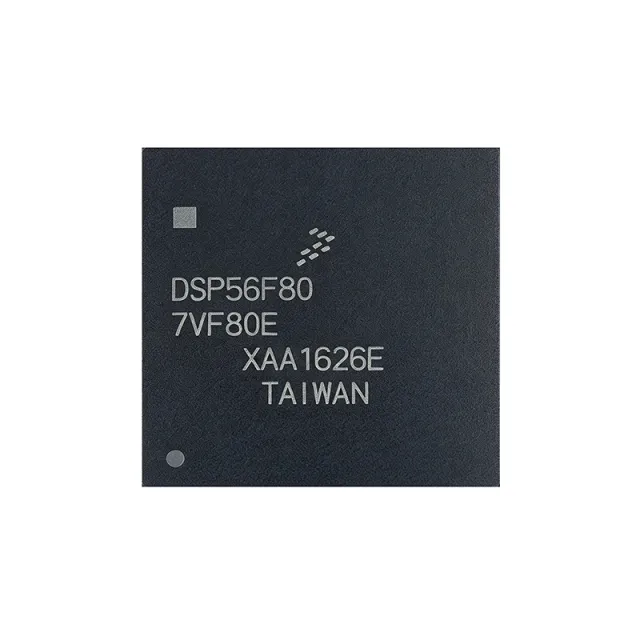
DSP56F807VF80E - 16-bit 56800 DSC 80MHz 160-MAPBGA | NXP
The NXP Semiconductors DSP56F807VF80E is a 16-bit Digital Signal Controller (DSC) based on the 56800 core, running at up to 80 MHz with 120KB (60K x 16-bit) of on-chip program flash memory, housed in a 160-ball MAPBGA (15x15 mm) package. As a member of the 56F8xx family, it combines DSP-class processing throughput with microcontroller-style peripherals on a single die. A Digital Signal Controller is a hybrid of a digital signal processor and a microcontroller: like a DSP it executes multiply-accumulate intensive control loops fast, and like an MCU it integrates flash memory, timers, communication interfaces, and ADCs for standalone embedded operation. In the semiconductor hierarchy, the DSP56F807VF80E sits within the digital signal controller category, under the broader families of digital signal processors, microcontrollers, and embedded processors. Key features include the Harvard-style 56800 architecture executing a 16-bit fixed-point instruction set with DSP addressing modes, up to 80 MHz core frequency for deterministic single-cycle MAC operations, 120KB of program flash, and support for up to 64K x 16-bit words (128KB) each of external program and data memory expansion per the manufacturer datasheet. The 3.3V supply domain and dense 160-ball MAPBGA footprint suit compact motor-control boards where board area is constrained. Architecturally, the 56800 core pairs a Harvard memory organization with microcontroller-friendly instruction set extensions, allowing C-compiled control code and hand-optimized DSP kernels to coexist. On-chip peripherals target servo and industrial drive topologies: PWM generation, analog-to-digital conversion, and serial communication, all synchronized to the 80 MHz core clock for low-latency current-loop control. Typical applications include servo motor control, industrial power inverters and converters, and digital power supplies, where the single-chip integration of DSP math and MCU peripherals reduces bill-of-materials cost versus a separate DSP-plus-MCU pairing. Design consideration: this part is End-of-Life per the NXP product page, so new designs should evaluate migration to the MC56F8xx successor family, and existing designs should secure last-time-buy inventory. This page synthesizes distributor pricing, datasheet references, EOL status, and replacement-strategy analysis not consolidated in the manufacturer datasheet.
DSP56F826BU80E - 16-Bit 80MHz DSC 64KB Flash | NXP
The NXP Semiconductors DSP56F826BU80E is a 16-bit hybrid Digital Signal Controller (DSC) from the 56800 core-based 56F8xx family, delivering up to 40 MIPS at an 80 MHz core frequency with 64KB (32K x 16) of on-chip Flash program memory, 4.5K x 16 of RAM, and 46 GPIO lines in a 100-pin LQFP (14 x 14 mm) package. A Digital Signal Controller combines the multiply-accumulate processing power of a DSP with the peripheral set and control-oriented functionality of a microcontroller on a single die. Within the system hierarchy, the DSC sits between a general-purpose MCU and a dedicated DSP, making it a natural fit for motor control, digital power conversion, and embedded signal-processing nodes that also require real-time control loops. Key features include hardware DO and REP loop instructions for zero-overhead looping, an MCU-friendly C-efficient instruction set, a quad timer module, a 4 MHz crystal oscillator with an integrated PLL including pre- and post-scalers, and serial connectivity via SCI (UART), SPI, and SSI (I2S-class) interfaces. The part is fabricated in high-density CMOS with 5V-tolerant, TTL-compatible digital inputs, allowing direct interfacing with legacy 5V logic on a 3.3V-domain board. Architecturally, the unified DSP/MCU core executes both signal-processing math and control flow from a single instruction set, eliminating the need for a two-chip DSP-plus-MCU solution. The on-chip Flash supports in-circuit reprogramming, and the JTAG/OnCE debug interface provides real-time non-intrusive debugging and flash programming through standard tools. Typical applications include industrial motor drives (BLDC, PMSM, AC induction), digital power supplies and inverters, and embedded control systems that require DSP-class filtering or FFT workloads alongside deterministic I/O timing. The quad timer and SSI make it well suited to multi-axis motion and audio-adjacent signal chains. A key design consideration: the part is End of Life per NXP, so new designs should plan a migration path, and existing designs should secure lifetime-buy inventory. Verify the 80 MHz timing closure at the full core frequency rather than assuming derated operation. This page synthesizes distributor pricing, drop-in alternatives, lifecycle notes, and practical design guidance not found in the manufacturer datasheet.
DSPA56367AG150 - 24-Bit Audio DSP 150MHz LQFP-144 | NXP
The NXP Semiconductors DSPA56367AG150 is a member of the DSP56300 family of programmable CMOS digital signal processors, featuring a 24-bit audio DSP core running at 150 MHz in a 144-pin LQFP (20x20 mm) package. It delivers up to 150 MIPS of processing throughput for embedded audio decoding, voice processing, and real-time signal conditioning. The device integrates program and data SRAM, an external memory interface, and on-chip peripherals tuned for consumer and professional audio equipment. A Digital Signal Processor (DSP) is a specialized microprocessor whose architecture is optimized for the mathematical operations common in real-time signal processing - multiply-accumulate (MAC) units, Harvard memory buses, and deterministic instruction cycles. Within the broader taxonomy, the DSPA56367 belongs to the category: DSP -> programmable CMOS DSP -> audio DSP -> embedded processor -> semiconductor IC. It sits alongside general-purpose microcontrollers but trades flexibility for raw signal-chain throughput and deterministic latency, which is critical when decoding compressed audio streams or running noise-cancellation loops. Key features include a 24-bit data word, up to 150 MIPS sustained throughput, dedicated audio I/O channels, a host interface (HPI/SCI), serial audio interface (SAI/ESSI), and a memory controller that supports external SDRAM and SRAM. The 144-pin LQFP-20x20 package provides ample I/O for multi-channel audio designs while using a standard surface-mount footprint and reflow-compatible lead finish. Architecturally, the DSP56367 uses a dual Harvard architecture with four internal data buses and one program bus, enabling single-cycle MAC operations. The 24-bit fixed-point data path provides extended dynamic range compared with 16-bit DSPs, reducing the need for intermediate scaling and yielding better headroom for audio codecs such as Dolby Digital, DTS, and AAC decoding. Typical applications include AV receivers, soundbars, automotive head units, professional audio mixers, and effects processors. Designers choose this family when deterministic real-time audio performance is required at production volumes. When designing with this part, ensure the JTAG/OnCE debugging interface is accessible on the PCB test fixture, and that the 3.3V core and I/O rails are sequenced correctly to avoid latch-up during brown-out events. This page synthesizes distributor pricing, drop-in alternatives, and practical design notes not found in the manufacturer datasheet.
DSPA56370AF - 24-bit DSP, 150MHz, Audio/Video | NXP/Freescale
The NXP (formerly Freescale Semiconductor) DSPA56370AF is a 24-bit, 150 MHz CMOS Digital Signal Processor (DSP) from the DSP56300 family, packaged for surface-mount integration in audio/video (AV) receivers, home theater systems, surround-sound decoders, mini stereo systems, digital TV audio systems, and automotive audio platforms. The DSP56371 (the datasheet-public sister part to the DSPA56370AF) is documented in the Freescale datasheet as a high-density CMOS device with 5.0 V-compatible inputs and outputs, and the DSPA56370AF is targeted at audio/video applications where 24-bit DSP precision is required. A digital signal processor (DSP) is a specialized microprocessor whose architecture - multiply-accumulate (MAC) units, Harvard memory buses, and zero-overhead looping - is optimized for numeric-heavy, real-time signal processing. The DSP56300 family belongs to the broader category of embedded processors > microprocessors > microcontrollers > semiconductors. DSPs sit between general-purpose microcontrollers (flexible but slower at numerics) and FPGAs (parallel but harder to program), and they dominate audio codecs, modem baseband, and control-loop workloads. Key features of the DSPA56370AF include the DSP56300 core running up to 150 MHz, 24-bit fixed-point data paths, on-chip memory configured for codec workloads, serial audio interfaces (ESSI), a host interface, and 5 V-tolerant I/O. The device targets audio decoding (Dolby, DTS, MPEG), sample-rate conversion, and parametric equalization. Its 24-bit word length preserves headroom for multi-channel downmix and dynamics processing without intermediate quantization artifacts. Architecturally, the device uses the Freescale/NXP DSP56300 Harvard architecture with dual memory banks and a dedicated address generation unit, allowing concurrent fetches of instruction and data words every clock cycle. The result is sustained MAC throughput matched to real-time audio codecs at typical 48 kHz / 96 kHz sample rates. Typical applications include AV receivers, home theater systems, surround-sound decoders, mini stereo systems, digital TV audio, and automotive audio head units where the DSP56300 core runs license-required surround decoding and EQ in real time. When designing with the DSPA56370AF, follow the Freescale/NXP DSP56300 hardware reference manual for SDRAM interface timing and JTAG boundary-scan configuration, and observe derating for VCC ripple during heavy codec decoding (typically < 50 mVpp on the analog supply rails). This page synthesizes distributor availability, datasheet references, and practical design considerations to support drop-in sourcing of the DSPA56370AF for AV-receiver platforms still in production or under long-term support.

DSPA56371AF150 - 150MHz 24-Bit Audio DSP | NXP Semiconductors
The NXP Semiconductors DSPA56371AF150 (DSP56371, 150 MHz version, DSPA371 grade) is a 24-bit audio digital signal processor (DSP) based on the DSP56300 family core, targeted at audio electronics system designers and supplied in a TQFP-80 surface-mount package. It is designed to run the latest generation of audio decoders including Dolby, THX and DTS, among others. A digital signal processor is a specialized microprocessor whose architecture is optimized for the fast, real-time mathematical operations required in digital signal processing, such as multiply-accumulate (MAC) filtering, Fourier transforms, and audio codec workloads. Within the signal-chain hierarchy, a DSP sits between general-purpose microcontrollers and fixed-function audio decoders, offering programmable flexibility with DSP-grade throughput. The DSP56371 belongs to the DSP56300 family -> embedded DSP -> digital signal processor -> semiconductor taxonomy. Key features include a 24-bit DSP56300 core executing at 150 MHz, an instruction set and on-chip peripherals specifically tailored for multichannel audio processing, and support for delay management, bass management and surround-sound decoding workloads described in the NXP product overview. The 24-bit data width matches the native word size of professional and consumer audio streams, avoiding truncation error in filter computations. Architecturally, the DSP56300 family uses a Harvard-style bus structure with separate program and data memory spaces and hardware MAC units, which sustains one multiply-accumulate per instruction cycle - the workhorse operation of audio IIR/FIR filtering and convolution. On-chip memory and serial audio interfaces allow direct connection to audio ADCs/DACs and receivers. Typical applications include audio/video (AV) receivers, home theater systems, surround-sound decoders, mini stereo systems, digital TV audio systems and automotive audio systems, per the official NXP product page. Design consideration: this device is End-of-Life per NXP, so new designs should secure lifetime stock or plan a replacement strategy before layout freeze; verify the current NXP discontinuance PCN before committing. This page synthesizes distributor pricing, drop-in same-family alternatives (DSPB56371AF150, DSPC56371AF180), and practical design notes not found in the manufacturer datasheet alone.
DSPA56371AF160B - 24-Bit 160MHz DSP QFP | NXP Semiconductors
The NXP Semiconductors (Freescale) DSPA56371AF160B is a 24-bit digital signal processor (DSP) core from the DSP56300 family of programmable CMOS DSPs, operating at a core clock frequency of 160 MHz and packaged in a QFP surface-mount package. This is the A-version marketable part number of the DSP56371 device, and per the NXP product page the part is designated End of Life (EOL). A digital signal processor is a specialized microprocessor architecture optimized for the high-speed mathematical operations required by real-time signal processing, such as multiply-accumulate (MAC) loops, filtering, and fast Fourier transforms. Within the semiconductor hierarchy, the DSP56371 sits under the DSP56300 family, the broader digital signal processor product category, and the general class of embedded processor ICs. The defining feature of the DSP56371 is its 24-bit fixed-point data path, which offers greater dynamic range than 16-bit DSPs while avoiding the cost and power of floating-point devices. According to the manufacturer documentation, the DSP56371 is a high-density CMOS device with 5.0-V compatible inputs and outputs, easing integration into legacy 5V board designs. The architecture includes on-chip memory, operating modes, and peripheral modules described in the DSP56371 reference manual. At 160 MHz, the DSPA56371AF160B is the highest-speed grade in this family, delivering the processing headroom required by demanding real-time control and signal-chain workloads. The device targets audio processing, telecommunications, motor control, and industrial signal conditioning applications, where deterministic multiply-accumulate throughput at 160 MHz and 24-bit precision directly improve system fidelity and control-loop accuracy. A key design consideration is that the part is End of Life. Designs still using this device should verify remaining authorized-distributor stock through channels such as DigiKey and TrustedParts, and evaluate last-time-buy quantities or redesign paths. Because the processor uses 5.0-V-compatible I/O, replacement candidates must match both the electrical interface and the QFP footprint. This page consolidates distributor availability, lifecycle status, and EOL replacement guidance for the DSPA56371AF160B that is not consolidated on the manufacturer product page, helping engineers plan obsolescence management actions efficiently.

DSPA56371AF180 - 24-bit Audio DSP, 180MHz, 80-LQFP | NXP
The NXP DSPA56371AF180 is a 24-bit fixed-point audio digital signal processor (DSP) from the DSP56300 family, running at 180MHz core clock (180 MIPS) in an 80-pin LQFP surface-mount package. It is part of NXP's Symphony audio DSP family, designed for next-generation home theater, AV receiver, automotive audio, and digital TV audio subsystems requiring Dolby, DTS, and THX decoder support. An audio DSP (Digital Signal Processor) is a specialized microprocessor optimized for high-speed numeric computation on continuous streams of audio samples. Audio DSPs sit beneath the broader hierarchy: DSP -> microprocessor -> integrated circuit -> semiconductor. Unlike general-purpose MCUs, audio DSPs use Harvard architectures, hardware MAC units, and deterministic instruction cycles to perform real-time decoding, mixing, and bass management without jitter or audible artifacts. Key features of the DSPA56371AF180 include 180 MIPS sustained throughput, integrated memory (ROM-masked firmware variant denoted by the 'A' suffix), hardware accelerated audio peripherals, and dedicated host and serial audio interfaces. The 180 MHz clock enables simultaneous multichannel decoding (e.g., 7.1 surround) plus post-processing while leaving headroom for proprietary algorithms. The 'AF' suffix indicates the 180 MHz speed grade and the Freescale/NXP automotive pedigree. Architecturally, the DSPA56371AF180 uses the DSP56300 core with parallel multiply-accumulate (MAC) units, dual-memory architecture (X and Y data, program memory), and a rich instruction set including fractional arithmetic. Compared to the earlier DSP56000 family, the DSP56300 adds enhanced DMA, larger on-chip memory, and improved peripherals for consumer audio. This combination delivers deterministic low-latency processing essential for lip-sync accuracy in AV receivers. Typical applications include AV receivers and home theaters, surround-sound decoders (Dolby Digital, DTS, THX), digital TV audio subsystems, mini-stereo systems, and automotive head units and infotainment audio. The Symphony firmware library integrated in masked-ROM variants enables rapid time-to-market for OEMs licensing certified decoders. When designing with this part, allocate sufficient PCB copper to the exposed pad (if present) and ensure clean 3.3V power with low-ESR decoupling to avoid jitter. Verify firmware revision compatibility between masked-ROM parts and external host MCU firmware before committing to production. This page synthesizes distributor pricing, drop-in alternatives, lifecycle status, and practical design notes for the DSPA56371AF180 not found in any single manufacturer datasheet or distributor page.
DSPA56720AG - Multi-Core 24-bit Audio DSP | NXP / Freescale
The NXP (formerly Freescale) DSPA56720AG is a multi-core 24-bit audio digital signal processor from the Symphony DSP5672x family, housed in a 144-pin LQFP (LFQFP) package. Built on multiple DSP56300 cores, the DSPA56720AG targets advanced audio applications including multi-channel decoding, encoding, and post-processing for home theater, automotive audio, and professional sound systems. The 'A' suffix and 'G' package designation identify the lead-free commercial-temperature LQFP-144 variant. What is a multi-core audio DSP? A digital signal processor (DSP) is a specialized microprocessor optimized for numerical operations on sampled analog signals. An audio DSP is tuned for low-latency, deterministic processing of audio frames using fixed-point arithmetic and hardware accelerators. The Symphony DSP5672x family combines two or more DSP56300 cores in a single die to deliver parallel processing of multiple audio streams and standards, bridging the gap between single-core DSPs and general-purpose processors in audio subsystems. Key features include 24-bit data paths, dual DSP56300 cores with hardware accelerators, integrated memory interfaces for external SDRAM, dedicated audio peripherals (serial audio interfaces, sample-rate converters), and the LFQFP-144 gull-wing surface-mount package with commercial temperature grade (0C to +70C). The architecture is programmable through NXP's Symphony Studio toolchain, and firmware libraries support popular codecs such as Dolby Digital, DTS, AAC, and MP3. From a technical standpoint, the DSPA56720AG is built on a 0.13-micron CMOS process, runs at clock speeds suitable for multi-channel HD audio, and supports heterogeneous memory mapping across internal SRAM and external SDRAM. The chip exposes multiple ESSI (Enhanced Synchronous Serial Interface) ports, a Host Interface (HI), and a peripheral control block for GPIO and interrupt management. Designers should consult the manufacturer datasheet for exact core clock, MIPS rating, and on-chip memory sizing. Typical applications include AV receivers, soundbars, automotive head units, and professional mixing consoles. The part is also deployed in broadcast audio equipment and consumer electronics where multi-channel decoding is required. When designing with the DSPA56720AG, allocate proper PCB thermal relief under the exposed pad of the LQFP-144 footprint, keep one quad high-speed ESSI traces short and impedance-controlled, and use NXP's Symphony Studio for firmware development. This page synthesizes distributor pricing, drop-in alternatives, and practical design notes not found in the manufacturer datasheet.
DSPB56364AF100 - 24-bit Audio DSP, 100MHz, 100-LQFP | NXP
The NXP DSPB56364AF100 is a 24-bit audio digital signal processor from the DSP56300 family, operating at 100 MHz and housed in a 100-pin LQFP (14x14 mm) package. It integrates a 24-bit data path, an enhanced filter coprocessor (EFCO), and on-chip memory optimized for cost-sensitive consumer audio processing. An audio DSP is a specialized microprocessor that performs mathematical operations on digitized audio signals in real time. Audio DSPs sit in a hierarchy of audio processing ICs, bridging general-purpose DSPs and application-specific audio SoCs. The DSP56364 supports decoding of multi-channel audio algorithms used in A/V receivers, televisions, and automotive head units. Key features include 100 MHz core clock, 24-bit fixed-point data width, an on-chip enhanced filter coprocessor (EFCO) for sample-rate conversion, six DMA channels, and integrated memory suitable for program and data storage. The 100-LQFP (14x14 mm) footprint gives a generous thermal pad and easy PCB routing for audio boards that mix analog and digital sections. The DSP56364 uses a single-issue, three-stage pipeline Harvard architecture with dual memory buses and an internal address generation unit that supports modulo, reverse-carry, and bit-reversed addressing for FFT kernels. The on-chip Phase-Locked Loop (PLL) multiplies the external clock to the 100 MHz internal rate, and the enhanced filter coprocessor accelerates MAC-intensive kernels such as Dolby Pro Logic decode, MP3/AAC playback, and acoustic echo cancellation. Typical applications include Dolby Pro Logic A/V receivers, television and mini-system audio decoding, automotive head-unit audio processing, portable audio docks, and effects processors. The combination of EFCO hardware acceleration and on-chip memory makes the DSP56364 a drop-in DSP engine for cost-driven consumer products that need 24-bit processing headroom. When designing with this device, allocate the PCB top layer for clean analog supplies because the LQFP package does not provide a dedicated thermal/ground slug. Place a 0.1 uF decoupling cap on each adjacent VCC/VDD pair, and keep the crystal trace shorter than 10 mm to meet the 100 MHz timing margin. This page synthesizes distributor pricing, drop-in same-family alternatives, and practical audio-board design notes that supplement the manufacturer datasheet.