IC Antarmuka
Subkategori
Produk (3.100+)

MCP2517FD-H/SLVAO - CAN FD SPI Controller | Microchip
The Microchip Technology MCP2517FD-H/SLVAO is an external CAN FD controller with an SPI interface, operating with the CAN 2.0 protocol at up to 8 Mbps and housed in a 14-pin SOIC package. It provides a compact way to add CAN FD communication to a microcontroller or other host processor that already has an SPI interface. The controller handles the CAN protocol functions while the connected host manages higher-level data exchange, configuration, and application processing. A CAN FD controller is a semiconductor interface device that converts data supplied by a host processor into frames suitable for transmission over a Controller Area Network bus. CAN FD extends conventional CAN operation with flexible data-rate capability, making the controller hierarchy useful for systems that need efficient payload transfer while retaining compatibility with a standardized CAN network architecture. The external SPI interface allows the controller to be paired with a broad range of microcontrollers rather than requiring a dedicated integrated CAN peripheral. The MCP2517FD-H/SLVAO combines three principal characteristics: CAN 2.0 support, an 8 Mbps maximum data rate, and a 14-pin SOIC package. The SPI host interface provides a straightforward connection to embedded processors, while the external CAN controller architecture separates bus protocol processing from the host MCU. This separation can simplify firmware partitioning and make it possible to upgrade communication capability on a board whose main processor lacks an adequate CAN controller. Technical implementation depends on the selected MCU SPI peripheral and the accompanying CAN transceiver. The MCP2517FD-H/SLVAO is a controller, not a physical-layer transceiver, so it requires a separate device such as the Microchip ATA6563 cited with the manufacturer’s MCP2517FD Click board. That board demonstrates the architecture by combining the MCP2517FD with an ATA6563 high-speed CAN transceiver to create a complete CAN node. Typical uses include industrial automation controllers, automotive body and gateway electronics, robotics, building equipment, and other embedded systems that need high-speed CAN FD connectivity. The SPI architecture is particularly useful when the host MCU has limited or no native CAN resources but can provide a suitable peripheral. Firmware still needs to initialize the controller, establish bit timing, configure filters, exchange status information, and manage interrupts or polling. Layout and firmware planning should treat the MCP2517FD-H/SLVAO as a timing-sensitive interface device. The SPI traces should be routed away from noisy switching nodes, the device should be placed close to its host and transceiver connections, and power and ground paths should be kept stable. Because the verified excerpts do not publish complete electrical limits, pin assignments, transceiver requirements, or ordering-code details, those items must be confirmed in the manufacturer datasheet before schematic or PCB sign-off. This page consolidates the verified manufacturer and distributor information, distinguishes controller versus transceiver roles, documents same-package family alternatives, and identifies missing electrical and pinout data without inventing specifications. It is intended to support initial component selection while directing engineers to the authoritative Microchip datasheet for final design validation.

MCP2517FDT-H/JHA - 8 Mbps CAN FD SPI Controller | Microchip
The Microchip Technology MCP2517FDT-H/JHA is a stand-alone CAN FD controller with an SPI interface, CAN 2.0 and CAN FD support, an 8 Mbps data rate, and a 14-VDFN package measuring 4.5 x 3 mm. It is designed to add CAN FD connectivity to a microcontroller that already provides an SPI peripheral. The controller operates as a serial peripheral and manages CAN frame transmission, reception, filtering, interrupts, and buffer storage while the host processor executes the network protocol and application layer. A CAN FD controller is a semiconductor that implements the Controller Area Network protocol below the host software layer. CAN FD extends classical CAN with flexible data payloads and higher communication throughput, while the SPI interface provides a compact connection to embedded processors. In the hierarchy, the MCP2517FDT-H/JHA belongs to CAN bus controllers, interface ICs, embedded semiconductors, and CAN communication devices. The verified distributor information identifies the device as an external CAN FD controller with SPI connectivity, CAN 2.0 operation, standby capability, transmit/receive support, a 14-VDFN package, and an 8 Mbps CAN rate. The controller also provides 2 KB of RAM for message storage and supports a 40 MHz CAN clock capability according to the supplied product description. These features make it useful where a host MCU lacks an integrated CAN FD peripheral or where modular CAN communication is preferred. The controller is appropriate for automotive gateways, industrial automation equipment, robotics, building controls, and embedded test systems. Its compact package helps reduce PCB area, while the external CAN transceiver remains a separate system component. The SPI connection also simplifies integration with common embedded processors, provided the host firmware correctly handles interrupts, acceptance filters, transmit queues, error states, and bus timing. Designers should follow the manufacturer datasheet for the exact electrical limits, oscillator requirements, transceiver interface, and exposed-pad layout. The CAN transceiver, crystal or clock source, termination, filtering, and firmware configuration must be validated together. Because the verified material does not provide complete timing, voltage, temperature, and pin-level data, those values are marked as data needed rather than inferred. This page combines verified distributor descriptions, manufacturer positioning, pricing availability, package information, and practical integration guidance. It is intended to help engineers identify whether this controller fits a CAN FD architecture before downloading the datasheet and validating the final PCB design.
MCP2517FDT-H/SL - 8Mbps CAN FD Controller | Microchip
The Microchip Technology MCP2517FDT-H/SL is an external CAN FD controller with an SPI interface, an operating voltage range of 2.7 V to 5.5 V, and a maximum CAN data rate of 8 Mbps in a 14-pin SOIC package. It adds CAN FD connectivity to a microcontroller or processor that already provides an SPI peripheral. A CAN FD controller is a protocol-specific interface integrated circuit that manages CAN frames and communicates with host processing logic through a register interface. CAN FD, or Controller Area Network with Flexible Data-rate, extends classical CAN with faster data phases and larger payloads. Within the broader semiconductor hierarchy, this device is an interface controller, a network-communications IC, and a peripheral for industrial, automotive, and embedded systems. The verified product information identifies automatic retransmission control, monitor mode, and low-power or standby operation as major operating features. The 8 Mbps maximum data rate suits communication links that need more throughput than classical CAN while retaining the CAN bus architecture. The 2.7 V to 5.5 V range supports both 3.3 V and 5 V system rails, although the complete host and transceiver design must satisfy the controller's electrical requirements. Unlike a combined CAN controller and transceiver, the MCP2517FDT-H/SL implements the protocol controller side of the link. It therefore requires a separate CAN transceiver, suitable bus protection, and a correctly designed PCB signal path. Its SPI host interface allows a microcontroller to configure bit timing, filters, interrupts, masks, and transceiver standby behavior through register access. Typical uses include vehicle network gateways, industrial automation controllers, battery-management systems, diagnostic equipment, elevator controls, robotics, and other embedded CAN FD nodes. Standby support can reduce power demand when a node does not need continuous bus participation, while monitor mode can support passive observation of bus activity. The principal design consideration is preserving signal integrity between the controller, external transceiver, connector, and termination network. Power decoupling should follow the manufacturer datasheet, and firmware must initialize the CAN FD bit timing, arbitration and data-phase timing, filters, interrupt routing, and error handling before enabling communication. This product record combines verified distributor specifications, sourcing information, comparison context, and practical integration guidance. It also distinguishes verified drop-in candidates from merely related CAN interface ICs, helping engineers avoid replacing a protocol controller with a functionally similar but pin-incompatible transceiver.
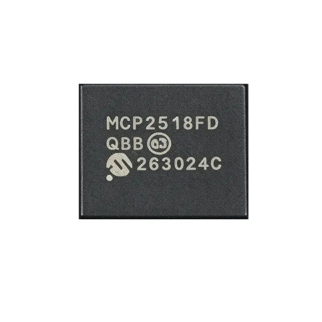
MCP2518FDT-E/QBB - CAN FD Controller, SPI, 14-VDFN | Microchip
The Microchip Technology MCP2518FDT-E/QBB is a stand-alone, low-power External CAN FD Controller with an SPI interface, housed in a 14-pin VDFN (4.5 mm x 3 mm) package with wettable flanks for automated optical inspection. It supports both Classical CAN 2.0B and CAN Flexible Data Rate (CAN FD) frames, enabling a cost-effective upgrade path for legacy CAN networks while delivering the higher payload and bit-rate advantages of CAN FD. The device integrates ECC-protected 2 KB RAM, dual maskable interrupt outputs, and grade-1 automotive temperature rating (-40C to +125C). A CAN FD Controller is a peripheral IC that handles the CAN/CAN FD protocol layer independent of the host microcontroller, exposing the bus as a register-mapped SPI slave. In the broader hierarchy, it sits above the physical-layer transceiver (such as the MCP2562FD) and below the application MCU; together these three blocks form a complete ISO 11898-1:2015 CAN node. Using an external controller lets designers add CAN FD to MCUs lacking an integrated CAN module, or offload protocol processing from low-power microcontrollers. Key features of the MCP2518FDT-E/QBB include up to 1 Mbit/s nominal CAN FD bit rate, 8 Mbit/s SPI clock support, low-power mode drawing approximately 10 µA typical, time-stamping via 32-bit TMR, and a wide operating voltage range of 2.7 V to 5.5 V. The VDFN-14 package occupies only 13.5 mm^2 of board area, making it the smallest CAN FD controller in Microchip's portfolio and ideal for space-constrained ECUs and sensor nodes. Architecturally, the MCP2518FD uses a dedicated CAN FD protocol engine plus RAM buffers, freeing the host MCU from bit-stuffing, arbitration, and CRC calculation. The SPI interface supports mode 0 and mode 3, with standard read/write commands plus a 16-bit CRC option on critical registers for EMI robustness. Combined with the external MCP2562FD high-speed transceiver, the resulting node is ISO 11898-1:2015 and ISO 11898-2:2016 compliant. Typical applications include automotive body and chassis networks, industrial CAN nodes (sensor hubs, motor drives), EV battery management (BMS) daisy chains, agricultural and off-highway vehicle telemetry, and any MCU-based system retrofitting CAN FD. The grade-1 (-40C to +125C) qualification makes it suitable for under-hood and chassis-mounted ECUs. When designing with this device, ensure the VDFN-14 exposed pad is soldered to a sufficiently large ground copper pour for thermal dissipation. A 100 nF decoupling capacitor must be placed within 5 mm of the VDD pin. The oscillator start-up time depends on the crystal load capacitance; consult the Microchip datasheet for matching network values. This page synthesizes distributor stock levels, parametric drop-in alternatives (including same-package Microchip variants), and PCB-layout guidance that is not consolidated on any single manufacturer or distributor product page.

MCP2551-E - 1Mb/s High-Speed CAN Transceiver, ISO-11898 | Microchip
The Microchip Technology MCP2551-E is a high-speed, fault-tolerant CAN (Controller Area Network) transceiver that serves as the physical-layer interface between a CAN protocol controller and the differential CAN bus, capable of operating at data rates up to 1 Mb/s and fully compliant with the ISO-11898 standard including 24V bus requirements, housed in an 8-pin SOIC (SN) package. The device provides differential transmit and receive capability for the CAN protocol controller, with a single 5V supply input (4.5V to 5.5V), an internal slope-control pin for selectable baud-rate modes, and a low-power standby mode current of roughly 275 µA typ. A CAN transceiver is the analog physical-layer bridge of any CAN bus, sitting between a digital CAN controller (such as the MCP2515) and the actual twisted-pair wiring harness. Its primary job is to translate the controller's TXD/RXD CMOS logic into the dominant/recessive differential voltage levels defined by ISO-11898, while absorbing ESD strikes, bus shorts, and load-dump transients so the fragile controller is never exposed to them. As a category, CAN transceivers fall under interface ICs in the broader semiconductor taxonomy of standard logic and bus-interface devices. Key features of the MCP2551-E include three operating modes (high-speed, slope-control for lower EMI, and standby) selected via the RS pin, a transmitter capable of driving a worst-case 45-Ω load (corresponding to a heavily-loaded bus with 64 nodes), automatic thermal-shutdown protection, and bus fault tolerance meeting the 24V automotive requirement. The VREF pin supplies a 0.5 × VCC reference useful for stabilizing the recessive level. Architecturally, the die uses a bipolar driver stage for robust bus-side drive strength, with CMOS logic on the controller-side pins. The driver's output impedance and the on-chip slope-control current source are trimmed at the wafer level to give predictable rise/fall times across temperature, which is important in automotive under-hood environments where the bus length and capacitance can vary widely. Typical applications include in-vehicle networking (OBD-II, body controllers, instrument clusters), industrial CANopen and DeviceNet links, and any 5V microcontroller system needing a standard ISO-11898 CAN port. Designers often pair the MCP2551-E with the MCP2515 controller (the same Microchip family) for a complete CAN node. When designing with the MCP2551-E, always place a 100 nF decoupling capacitor close to VCC and provide a common-mode choke plus a 120 Ω termination resistor at each end of the bus. The part is now being superseded by the AEC-Q100-qualified MCP2561 for new automotive designs, but remains widely available and fully supported for industrial and legacy systems. This page consolidates Microchip datasheet specifications, drop-in SOIC-8 alternatives such as the MCP2561 and TI SN65HVD251, and field-level design guidance not found in a quick distributor lookup.

MCP2551-E-P - 1 Mbps Fault-Tolerant CAN Transceiver
The Microchip Technology MCP2551-E-P is a 1 Mbps high-speed CAN physical-layer transceiver with one transmitter and one receiver, a 4.5 V to 5.5 V supply range, and an 8-pin DIP package. It provides the physical interface between a CAN protocol controller and the differential CAN bus while supporting fault-tolerant operation in 12 V and 24 V systems. According to the supplied data, it implements ISO-11898 physical-layer requirements and uses externally controlled slope to reduce radio-frequency interference. A CAN transceiver is an interface IC that converts logic-level controller signals into the differential physical signaling used by a Controller Area Network. The MCP2551-E-P belongs to the hierarchy CAN transceiver > bus interface > interface IC > semiconductor. This device combines a CAN driver, CAN receiver, bus-fault handling, standby control, and a reference output in one physical-layer device. Its principal features include 1 Mb/s operation, one driver and one receiver, 4.5 V to 5.5 V operation, and suitability for 12 V and 24 V systems. Externally controlled slope is especially useful when electromagnetic compatibility must be balanced against bus timing. Fault tolerance is a core function because automotive and industrial CAN buses can experience wiring faults and abnormal bus conditions. The MCP2551-E/P designation identifies the through-hole 8-pin DIP format in the supplied distributor data. It is intended for designs using a CAN controller with a logic-side interface and a differential CANH/CANL bus connection. The package and protocol role make it relevant to automotive electronics, industrial automation, robotics, embedded control, and instrumentation. A key design consideration is that CAN bus implementation depends on correct termination, common-mode behavior, transceiver wiring, controller compatibility, and PCB or harness layout. The verified search data identifies the device as fault tolerant and capable of 1 Mb/s operation, but detailed loop-delay, propagation-delay, receiver-threshold, and absolute-maximum-rating values were not supplied. Those values should be taken from the manufacturer datasheet before final timing or protection design. This page synthesizes the supplied distributor and manufacturer-search data, package information, CAN use cases, replacement considerations, and practical design guidance. It does not infer undocumented electrical limits or assume regulatory compliance.
MCP2551-E/SN - High-Speed CAN Transceiver 1Mbps SOIC-8 | Microchip
The Microchip Technology MCP2551-E/SN is a high-speed CAN (Controller Area Network) transceiver in an 8-pin SOIC (SN) package, providing the physical interface between a CAN protocol controller and the differential bus. It supports data rates up to 1 Mbps and is fully compatible with the ISO-11898-24V standard, including 24V bus fault protection. Operating from a single 4.5V to 5.5V supply, it is a 1/1 (one transmitter, one receiver) half-duplex transceiver. A CAN transceiver is the analog physical-layer device that converts the digital TX/RX logic signals from a CAN controller (such as the MCP2515) into the differential voltage levels required on a CAN bus. The CAN protocol itself is defined by ISO 11898 and is widely used in automotive (CAN, CAN-FD), industrial (CANopen, DeviceNet), and medical equipment because of its robust differential signaling, built-in arbitration, and reliable behavior in electrically noisy environments. Transceivers like the MCP2551 sit in the hierarchy: physical-layer transceiver -> CAN controller -> host MCU -> application layer. Key features include slope control for reduced EMI (selectable via the RS pin), a low-power standby mode (pin S1), thermal shutdown protection, short-circuit protection on the bus pins (CANH/CANL) to battery and ground, and an internal VREF output for biasing split termination. The device survives load-dump events up to ±40V on the bus pins, exceeding the ISO-7637 transient specification. Up to 112 nodes can be connected to a single CAN bus segment. Typical applications include automotive body and chassis networks, industrial CANopen and DeviceNet nodes, building automation (BACnet), fleet management and telematics, and any embedded system that needs ISO-11898-compliant differential CAN communication. The 5V VCC and 8-pin SOIC footprint also make it a convenient drop-in upgrade for legacy MCP2551 designs being migrated to longer lead-time alternatives. When designing with this device, place a 100nF decoupling capacitor close to VCC and use a split termination network (typically 120 ohm total with two 60 ohm resistors and a 10nF capacitor to ground) to match the bus impedance and suppress common-mode noise. Ensure the RS pin is tied to ground for high-speed mode or through a resistor to slow the slew rate if EMI is a concern.
MCP2551-I - High-Speed CAN Transceiver, 1 Mb/s, 8-Pin DIP/SOIC | Microchip
The Microchip Technology MCP2551-I is a high-speed CAN (Controller Area Network) fault-tolerant transceiver that interfaces a CAN protocol controller to the physical bus, operating at data rates up to 1 Mb/s in an 8-pin PDIP or SOIC package. It provides differential transmit and receive capability, is fully compatible with the ISO-11898 standard, and meets the 24V automotive bus requirement. The device supports a supply voltage range of 4.5V to 5.5V and is designed for harsh industrial and automotive environments. A CAN transceiver is a physical-layer device that translates the digital transmit/receive signals from a CAN controller into the differential voltage levels (CANH/CANL) required on the bus. It belongs to the broader hierarchy of interface ICs, sitting between protocol controllers (such as MCP2515 standalone CAN controllers) and the physical wiring harness, and ultimately forms part of the in-vehicle or industrial networking infrastructure. CAN transceivers like the MCP2551-I are the bedrock of automotive OBD-II, CANopen, and DeviceNet networks. Key features include ±80V bus fault protection on CANH and CANL, a high-noise immunity design (>1V common-mode range), thermal shutdown protection, and an automatic thermal slope control that reduces emissions at lower data rates. The device has three operating modes: High-Speed, Slope-Control, and Standby, with the mode selected via the RS pin. A VREF output (2.5V typical) is provided as a voltage reference for the CAN controller. The MCP2551-I uses a bipolar process technology and incorporates slope control to minimize EMI by limiting the rise/fall times of CANH and CANL. Its differential receiver provides excellent noise immunity with a typical hysteresis of 100 mV. The transceiver operates across -40°C to +125°C industrial temperature range, making it suitable for under-hood automotive and rugged industrial applications. Typical applications include automotive body and chassis networks, industrial CANopen and DeviceNet nodes, OBD-II vehicle diagnostics, HVAC and elevator control systems, and medical instrumentation interconnects. Designers frequently pair the MCP2551-I with the MCP2515 standalone CAN controller for full CAN node implementations. A critical design consideration is bus termination: the CAN bus requires 120 Ω resistors at each end of the bus segment, and these are typically not integrated in the MCP2551-I. The RS pin should be tied high through a resistor to VCC for high-speed operation or connected to ground through a resistor to enable slope-control mode for lower EMI at reduced data rates. This page synthesizes distributor pricing, drop-in alternatives, and practical design notes not found in the manufacturer datasheet alone, including cross-brand equivalents and pin-compatible migration paths to the MCP2561.
MCP2551-I/P - 5V High-Speed CAN Transceiver DIP-8 | Microchip
The Microchip MCP2551-I/P is a high-speed CAN (Controller Area Network) protocol transceiver in an 8-pin PDIP (P) package, operating from a 4.5V to 5.5V single supply. It provides differential transmit and receive capability between a CAN protocol controller and the physical two-wire bus, supporting data rates up to 1 Mb/s per ISO-11898. The device includes slope-control input for selectable high-speed or slope-controlled (lower EMI) operation, a standby pin for low-power mode, and a VREF output for internal reference. A CAN transceiver is a physical-layer interface IC that bridges a digital CAN controller (typically a microcontroller with a CAN module) and the differential CAN bus wiring. It converts single-ended TXD logic into differential bus voltages on transmit, and converts differential bus voltages back into single-ended RXD logic on receive. CAN transceivers are the physical foundation of robust in-vehicle networking and industrial fieldbuses, and they are governed by the ISO 11898 family of standards. Key features of the MCP2551-I/P include: 1/1 (one driver, one receiver) half-duplex topology, 200 mV receiver hysteresis for noise immunity, thermal shutdown protection, short-circuit protection to battery and ground on the bus pins (up to ±40 V), and an operating temperature range of -40C to +85C (the "I" industrial grade). The device is widely deployed in automotive ECUs, industrial CAN nodes, building automation, and any embedded system that requires ISO 11898 compliant physical-layer connectivity. The MCP2551-I/P uses a bipolar architecture with internal slope control to limit EMI from the bus driver edge rates. The receiver inputs feature high common-mode range so the part tolerates ground offset between nodes. In addition, the device includes a VREF pin for a stable mid-supply reference voltage that older controllers require, making it a backwards-compatible choice for legacy CAN designs. Typical applications include automotive body and chassis ECUs, industrial CANopen and DeviceNet nodes, OBD-II diagnostic interfaces, agricultural machinery networks, and elevator or building automation controllers. Because the part is in a through-hole PDIP-8 package, it is also commonly used in prototyping, education kits, and hobby robotics (e.g. Arduino CAN shields) where through-hole assembly is preferred. When designing with the MCP2551-I/P, observe ISO 11898 bus termination requirements: a 120 ohm termination resistor at each end of the bus, twisted-pair cabling, and adequate common-mode choke or ESD protection for harsh environments. Also note that Microchip's newer MCP2561/2 family is the recommended migration path for new designs. This page synthesizes distributor pricing, drop-in alternatives, and practical design notes not found in the manufacturer datasheet.
MCP2551-I/SN - High-Speed CAN Transceiver, 1Mb/s, ISO-11898 | Microchip
The Microchip Technology MCP2551-I/SN is a high-speed Controller Area Network (CAN) protocol transceiver that serves as the interface between a CAN protocol controller and the physical differential bus, operating at speeds up to 1 Mb/s. The device is supplied from a single 4.5 V to 5.5 V rail, packaged in an 8-pin SOIC (SN) with industry-standard pinout, and provides differential transmit and receive capability to the bus. It is fully compatible with the ISO-11898 standard physical-layer requirements, including the 24 V load specification, making it suitable for both 12 V and 24 V automotive and industrial systems. A CAN transceiver is a physical-layer (PHY) device that converts the single-ended TTL-level transmit (TXD) and receive (RXD) signals of a CAN controller into the differential CAN_H and CAN_L signals driven on the bus. Transceivers such as the MCP2551 provide the dominant/recessive arbitration signaling, bus biasing, ESD protection, and fault tolerance needed by the differential multi-drop CAN bus used in automotive and industrial networking. They sit between the bus and protocol controllers such as the Microchip MCP2515 or the MCU-integrated CAN modules on dsPIC, PIC18, and many ARM Cortex-M microcontrollers. Key features of the MCP2551-I/SN include 1 Mb/s maximum data rate, externally-controlled slope (rise/fall) adjustment for reduced RFI, a low-current standby mode, a VREF output for the CAN controller's input reference, and detection of permanent bus dominant faults with automatic recovery to receiver-only mode. The device also supports the -2 V to +7 V common-mode range required by ISO-11898-2 (extended common-mode versions go further) and includes thermal shutdown and current limiting on the bus pins for bus-fault protection. Architecturally, the MCP2551 uses an NMOS differential driver on the bus side with slope control implemented by varying the driver output current; a bandgap-based VREF generator provides a 2.5 V (typical) reference for the RXD comparator threshold generation inside the controller. Internal hysteresis and input filtering suppress RF and transient noise on CAN_H/CAN_L without delaying the bit time, which preserves CAN arbitration timing at the maximum 1 Mb/s data rate. Typical applications include automotive body and powertrain networks, industrial CAN-based control systems (CANopen, DeviceNet, NMEA 2000), building automation, HVAC controls, and any embedded design using a Microchip MCU with a CAN module. Its 8-SOIC footprint and 5 V supply make it easy to add a CAN physical layer to existing 5 V designs. Note: per Microchip's discontinuance notices, the MCP2551 in SOIC-8 (SN) is being phased out, so verify stock and review the recommended MCP2561/2562 successor family for new designs. When designing with this device, observe CAN bus termination: place 120 ohm resistors at each END of the bus (not at every node), and use twisted-pair cabling. Provide a small decoupling capacitor as close as possible to VDD (pin 3) and tie the unused RS pin (pin 8) to GND through a resistor (or directly) to select normal high-speed slew rate. This page synthesizes distributor pricing, drop-in alternatives, and practical PCB/CAN-bus design notes not found in a single manufacturer datasheet.
MCP2551T-E/SN - 1Mbps Fault-Tolerant CAN | Microchip
The Microchip Technology MCP2551T-E/SN is a high-speed, fault-tolerant CAN transceiver operating up to 1 Mb/s, supplied from 4.5 V to 5.5 V and housed in an 8-pin SOIC package. It provides one differential CAN driver and one differential receiver, forming the physical-layer interface between a CAN protocol controller and a 12 V or 24 V CAN bus. The device supports the ISO-11898 physical-layer requirements, including the stated 24 V requirement, and its industry-standard 8-SOIC pinout supports surface-mount PCB assembly. A CAN transceiver, also called a CAN physical-layer interface, converts logic-level TXD and RXD signals into the dominant and recessive voltage states used on a differential CAN network. It bridges a host CAN controller and the physical bus while providing fault-tolerant behavior for automotive, industrial, and embedded systems. The MCP2551 family is positioned above simple logic transceivers because it addresses bus termination, common-mode operation, radiated emissions, and protection in connected vehicle or machine environments. Key verified features include support for 1 Mb/s operation, differential transmit and receive, ISO-11898 physical-layer compatibility, suitability for 12 V and 24 V systems, and externally controlled slope for reduced RFI emissions. The supplied datasheet also describes ground-fault detection for a permanent dominant condition on the TXD input. These features help a system control edge rate, recognize abnormal bus states, and reduce electromagnetic interference while retaining a conventional controller interface. The MCP2551 is a 1/1 CAN transceiver: one driver and one receiver are combined in one package. Its 4.5 V to 5.5 V supply range matches conventional 5 V CAN-controller ecosystems. At the physical bus, the differential CANH and CANL conductors carry complementary signals, while the transceiver interfaces to the controller through TXD and RXD. The exact logic levels, propagation delays, receiver thresholds, and absolute maximum ratings should be read from the manufacturer datasheet before final sign-off. Typical uses include automotive diagnostic links, industrial automation equipment, elevator and building-control networks, robotics, embedded motor-control systems, and CAN-based sensor or actuator networks. The 1 Mb/s capability is appropriate for high-rate short CAN networks, while the external slope-control option allows the designer to tune emissions behavior to the PCB and cabling environment. The 8-SOIC package also makes the device convenient for surface-mount designs that need a separate physical-layer transceiver beside a host microcontroller. Designers should pay attention to bus termination, transceiver supply decoupling, common-mode grounding, and the CAN controller's timing requirements. Place the termination network at the physical ends of the bus rather than beside every node. Review the datasheet's TXD, RXD, VDD, GND, CANH, and CANL connections and verify the selected logic family and package variant before manufacture. The MCP2551T-E/SN data should be treated as the authoritative source for values not explicitly stated in the verified search results. This page consolidates the verified MCP2551T-E/SN specifications, source links, application guidance, and replacement considerations. Pricing is shown as reference data as of 2026-10-22 where supplied by the verified distributor result; current commercial availability should be confirmed directly with the seller.
MCP2551T-I/SN - 1 Mb/s CAN Transceiver | Microchip
The Microchip Technology MCP2551T-I/SN is a 1 Mb/s high-speed CAN transceiver operating from a 4.5 V to 5.5 V supply in an 8-pin SOIC package. It provides one differential transmitter and one differential receiver between a CAN protocol controller and the physical CAN bus, with fault tolerance and compatibility with ISO-11898 requirements, including 24 V bus conditions. Its 5 V interface and 8-SOIC construction suit conventional embedded CAN nodes requiring a direct logic-side transceiver connection. A CAN transceiver is the physical-layer interface between a CAN controller and a multidrop differential bus. The controller generates and interprets CAN frames, while the transceiver converts controller logic into dominant and recessive differential states and converts bus differential voltage into a readable receive signal. This separation allows a microcontroller or dedicated CAN controller to implement the protocol while the MCP2551 handles bus-level voltage, noise immunity, and fault containment. Key verified characteristics include differential transmit and receive, operation up to 1 Mb/s, a 4.5 V to 5.5 V supply range, ISO-11898 compatibility including 24 V requirements, and fault-tolerant operation. The T-I/SN ordering code identifies the 8-pin SOIC, industrial-temperature, tape-and-reel ordering configuration; the verified distributor result describes the device as one transmitter and one receiver in an 8-SOIC package. The MCP2551 family is suitable for industrial automation, automotive electronics, embedded control, instrumentation, and other CAN networks operating with a 5 V transceiver supply. Designers should still validate the complete system against its required ISO-11898 revision, bus topology, termination, fault behavior, EMC requirements, and controller timing. The manufacturer datasheet is the controlling source for absolute maximum ratings, DC and AC electrical characteristics, timing, dimensions, and detailed application guidance. Use a 5 V regulated transceiver rail, connect the controller TXD and RXD pins according to the datasheet, and terminate the differential bus at both physical ends with the resistance specified by the selected bus standard. Keep the CANH and CANL routing as a controlled differential pair, provide a solid ground reference, and avoid long unprotected stubs. Decoupling should follow the manufacturer recommendations and be placed close to the supply pins. The key engineering trade-off is that this is a classic 5 V SOIC transceiver rather than a smaller, lower-voltage or automotive-packaged alternative. The result is useful because it combines a straightforward controller interface, established CAN physical-layer behavior, and compact 8-pin packaging. This page consolidates verified source links, commercial availability information, replacement constraints, and practical PCB guidance that should be checked against the latest manufacturer documentation before release to production.
MCP2562-E/SN - 1Mbps CAN Transceiver, 5V | Microchip
The Microchip Technology MCP2562-E/SN is a 1 Mbps high-speed CAN transceiver with a 4.5 V to 5.5 V supply range and an 8-pin SOIC package. It provides one CAN transmitter and one CAN receiver, bridging a CAN protocol controller to a physical two-wire CAN bus. A dedicated VIO supply supports direct interfacing with microcontrollers operating from 1.8 V to 5.5 V. A CAN transceiver is an interface IC that converts logic-level controller signals into the dominant and recessive voltage states used on a CAN bus, while converting bus states back into controller-compatible receive data. The MCP2562 family is commonly used in the CAN interface layer between a host microcontroller, CAN controller, vehicle network, industrial automation system, or embedded diagnostic equipment. The verified product information identifies the MCP2562-E/SN as a 1 Mbps CAN transceiver with a 5 V operating supply and an 8-pin SOIC package. Its separate VIO pin reduces the need for external level shifters when the CAN controller uses a lower-voltage IO domain. The device also supports standby control and undervoltage-related bus-management functions according to the product description sources. The MCP2562-E/SN is suitable for high-speed CAN networks requiring a compact surface-mount solution. Its 1 Mbps data rate supports automotive and industrial communication systems, while the dedicated VIO supply helps simplify connections to modern low-voltage microcontrollers. The 8-SOIC package also facilitates conventional PCB assembly and inspection. Typical applications include automotive engine-control modules, body electronics, industrial controllers, robotics, CAN-based sensor networks, diagnostic equipment, and embedded communication gateways. Designers should verify pin compatibility, transceiver mode behavior, supply sequencing, bus termination, and EMC requirements before replacing another CAN transceiver. This page combines verified distributor and manufacturer-derived product facts, structured specifications, application guidance, design notes, and same-footprint alternatives. Exact operating-temperature limits, loop-delay values, ESD ratings, and pin-level electrical limits require confirmation from the manufacturer datasheet before design release.
MCP2562FD-E/SN - CAN FD Transceiver, 8-SOIC | Microchip
The Microchip Technology MCP2562FD-E/SN is a second-generation high-speed CAN Flexible Data Rate (CAN FD) transceiver that interfaces a CAN protocol controller to the physical two-wire CAN bus, housed in an 8-pin SOIC (SN) package. It supports data rates up to 8 Mbps in CAN FD mode, 5 Mbps in classic CAN mode with high-speed slew rate, and operates over a VIO supply range of 1.8V to 5.5V for direct MCU interface. Key features include a maximum loop delay of 130 ns and guaranteed loop delay symmetry to support CAN FD bit timing requirements. The device operates across an ambient temperature range of -40C to +125C and survives load dump transients up to +/- 70V on the bus pins through integrated protection. A CAN transceiver serves as the physical-layer interface between a CAN protocol controller (such as the MCP2518FD or integrated CAN module on a microcontroller) and the differential CAN bus (CANH/CANL). It translates the controller's transmit (TXD) and receive (RXD) digital logic into the differential bus signaling defined by ISO 11898-2:2016, and provides the dominant and recessive states needed for non-destructive bitwise arbitration. CAN FD extends the classic CAN payload from 8 bytes to 64 bytes while remaining backward-compatible at the physical layer, which is why FD-compliant transceivers like the MCP2562FD are now preferred even for classic CAN designs. The MCP2562FD delivers 5 key advantages. First, the integrated VIO pin eliminates level shifters when interfacing 1.8V/3.3V MCUs. Second, low loop-delay symmetry (<=130 ns total) enables reliable 2 Mbps and 5 Mbps CAN FD operation. Third, +/- 36V receiver common-mode range tolerates large ground shifts across nodes. Fourth, +/- 70V bus-pin transient protection (IEC 61000-4-2 ESD and load dump) eliminates external TVS diodes in most automotive 12V/24V systems. Fifth, an ultra-low-current standby mode (~15 uA typical) preserves battery life in always-bus-wake applications. The MCP2562FD uses a 1.8V to 5.5V VIO supply rail that sets the logic level reference for TXD, RXD, and the standby (STBY) pin, while the VCC/VSUP rail (4.5V to 5.5V) powers the bus-side driver. An on-chip LDO from VCC to VIO is provided on the -H variants; the -E/SN variant requires the user to supply VIO externally for maximum flexibility. The integrated slope-control circuitry automatically adjusts the CANH/CANL edge rate to meet ISO 11898-2:2016 at any speed between 50 kbps and 5 Mbps, so no external resistor selection is required. Typical applications include automotive gateway ECUs, body-control modules, ADAS sensor CAN buses, industrial PLC networking, agricultural machinery CAN backbones, and any battery-powered remote sensor that needs an always-listening low-power mode. It also suits prototypes and maker projects using boards such as the Teensy, Arduino, and Raspberry Pi that need a CAN shield with simple 3.3V logic. When designing with this device, route the CANH/CANL traces as a 120-ohm differential pair with characteristic impedance of 120 ohms and place a 120-ohm termination resistor at each end of the bus; place a 100 nF decoupling capacitor as close as possible to the VCC and VIO pins to suppress switching noise from the bus driver. This page synthesizes distributor pricing, drop-in cross-brand alternatives, and practical layout guidance not found in the manufacturer datasheet.
MCP41010-I/P - 8-Bit 10kΩ SPI Digital Potentiometer
The Microchip Technology MCP41010-I/P is a single-channel, 8-bit digital potentiometer with 10 kΩ end-to-end resistance, 256 taps, and an SPI serial interface in an 8-pin PDIP package. It replaces a mechanical potentiometer with a digitally controlled resistance whose wiper position varies linearly according to commands written over the serial bus. A digital potentiometer is a solid-state variable resistor whose effective tap position is stored in an internal register. The MCP41010 belongs to the digital potentiometer, programmable resistor, interface IC, and power-management-adjacent control-device hierarchy. Its SPI interface allows a microcontroller to adjust gain, offset, current, voltage, or resistance without mechanical wear, while preserving a familiar three-terminal potentiometer arrangement. The device provides 256 wiper positions, giving an 8-bit command resolution and a linear relationship between the programmed code and resistance. Its 10 kΩ end-to-end resistance is suitable for signal-conditioning, current-control, and calibration networks where a compact, digitally adjustable resistance is required. The MCP41010 is controlled through standard SPI serial commands and supports integration with embedded control systems. Because the MCP41010 has only one potentiometer channel and one wiper, it is intended for single-axis adjustment rather than multi-channel gain or timing control. Its SPI architecture makes it suitable where board space is constrained and repeated electronic recalibration is more valuable than the mechanical travel and resolution of a conventional potentiometer. Applications include sensor calibration, programmable gain, current feedback, test equipment, audio attenuators, and embedded control systems. Designers should treat the terminals A, B, and W as the functional equivalent of a potentiometer while accounting for the internal wiper resistance and finite bandwidth. Place the device close to the controlled signal path, use a defined ground reference, and keep sensitive SPI routing away from high-current switching nodes. Software should limit wiper movement when a mechanical load could otherwise stall the internal wiper. This page combines the manufacturer's product information with practical application guidance, interface comparisons, and design notes. It helps engineers assess the MCP41010-I/P as an SPI-controlled 10 kΩ digital resistor for embedded analog-control designs, while separate handling of lifecycle, compliance, and sourcing details keeps the page suitable for technical evaluation and quotation.
MCP41050-E/P - 50k SPI Digital Potentiometer | Microchip
Microchip Technology MCP41050-E/P is a single-channel, 8-bit digital potentiometer with 50 kΩ end-to-end resistance, 256 wiper positions, and a 3-wire SPI interface in an 8-pin PDIP package. It operates from 2.7 V to 5.5 V and provides a software-programmable resistance or attenuation function without a mechanical wiper. A digital potentiometer is a programmable resistor whose effective tap position is stored as an 8-bit code. The MCP41050-E/P places one digitally controlled resistor between two analog terminals and presents a wiper output. This digital potentiometer belongs to the MCP41XXX family of single-channel, 256-position devices and sits within the broader category of passive analog components controlled by interface ICs. The principal benefits are 8-bit resolution, 256 discrete wiper settings, and SPI-based control. The wiper position varies linearly with the code written to the device, making the MCP41050-E/P useful for programmable gain, attenuation, bias adjustment, threshold setting, sensor calibration, and feedback-loop compensation. Its 50 kΩ resistance provides a practical balance between divider precision, signal range, and component loading. The device supports a 2.7 V to 5.5 V supply range and uses a serial interface that allows the wiper code to be updated by a host controller. Its maximum integral nonlinearity is specified as ±1 LSB, while the 256-position architecture corresponds to 8-bit resolution. The -E device variant is supplied in a through-hole PDIP package, making it convenient for prototypes, educational boards, and assemblies that favor socketed or leaded components. Typical applications include audio volume and attenuation control, sensor signal conditioning, programmable reference circuits, laboratory equipment, industrial control modules, and microcontroller-based instrumentation. Because the resistance changes under digital control, the part can eliminate electromechanical potentiometers where reliability, repeatability, or remote adjustment matters. When laying out a circuit, route the SPI signals away from sensitive analog inputs, keep the wiper connection short, and treat terminal resistance, wiper impedance, and the load connected to the wiper as part of the signal-path design. Confirm the programmed resistance against the required transfer function, because the ideal 8-bit relationship does not remove the effects of finite output resistance and load error.
MCP41050-I/P - 50kOhm 8-Bit SPI Digital Potentiometer | Microchip
The Microchip Technology MCP41050-I/P is a single-channel, 8-bit digital potentiometer with 50 kΩ end-to-end resistance, 256 SPI-addressable tap positions and a linear wiper taper, housed in an 8-pin PDIP package. It operates from a 2.7 V to 5.5 V supply voltage and supports SPI clock modes 0,0 and 1,1. A digital potentiometer is a solid-state, actively controlled substitute for a mechanical trimmer potentiometer. Instead of a sliding wiper driven by a screw or shaft, it uses an internal resistor string terminated by an electrically driven wiper that is positioned by a serial command. In the broader component hierarchy it sits above the passive potentiometer and alongside the resistor network, and it belongs to the family of programmable passives used to trim, calibrate or attenuate a signal without physical adjustment. Key features of the MCP41050 include 256 taps per potentiometer, ±1 LSB maximum integral nonlinearity and differential nonlinearity, a low-power serial interface, and an end-to-end resistance of 50 kΩ. The part belongs to the MCP41XXX/MCP42XXX family, which offers single and dual channel versions in 10 kΩ, 50 kΩ and 100 kΩ resistance options, so the same firmware and board pattern can be reused across different trim ranges. The device uses a serial peripheral interface (SPI) compatible command structure for writing the wiper register, which lets a microcontroller set the tap position in a single byte transfer. The wiper position is held in a volatile register, meaning the last programmed value is retained while power is applied but returns to a defined state after power cycling. The MCP41XXX device is a single-channel part offered in 8-pin PDIP and SOIC packages, with outstanding AC and DC characteristics for audio and instrumentation signal paths. Typical applications include audio volume and gain control, sensor amplifier calibration, programmable filter and threshold adjustment, and general instrumentation trimming where a fixed value must be set by firmware rather than by hand. Because the wiper position is controlled in software, calibration data can be stored in non-volatile memory and reloaded on every power-up. When designing with the MCP41050-I/P, remember that the wiper is not a buffered output: place a buffer or a suitable feedback resistor network after the wiper pin when driving a high-impedance or capacitive load. Also allow for the potentiometer's own resistance in the signal path and keep the SPI traces short, since the interface is sensitive to ringing on fast clock edges. This page brings together device specifications, pin-level detail, package-level alternatives and practical design notes that go well beyond the basic parameter table, helping engineers qualify the MCP41050-I/P for new designs without repeated datasheet searching.
MCP41100-I/P - 100kΩ 8-Bit SPI Digital Potentiometer | Microchip
Microchip Technology MCP41100-I/P is a single-channel, 8-bit digital potentiometer with a 100 kΩ end-to-end resistance, 256 wiper positions, and a 3-wire SPI serial interface in an 8-pin PDIP package. The wiper position varies linearly with the value written to the wiper register, allowing an external controller to adjust resistance without a mechanical potentiometer. A digital potentiometer is a solid-state resistor whose effective resistance or voltage-divider tap is controlled electronically. The MCP41100 belongs to the digital potentiometer hierarchy, combining a resistor array, switch matrix, wiper circuitry, and serial interface in one integrated circuit. This eliminates moving contacts, improves repeatability, and supports remote configuration through a microcontroller or embedded control system. The MCP41100-I/P provides 8-bit resolution across 256 positions, a 100 kΩ nominal end-to-end resistance, and SPI control. Its linear wiper characteristic simplifies calculations when the device is used as a voltage divider, a programmable attenuation element, or an adjustable resistance in control and measurement circuits. The 8-bit interface also allows the controller to select a position using an 8-bit command word. The device uses a 3-wire serial interface compatible with the SPI communication format identified by Microchip for the MCP4XXXX family. The target MCP41100-I/P is supplied in the 8-pin PDIP package, allowing through-hole assembly and prototyping. For compact production boards, the manufacturer also offers MCP41100 variants in surface-mount packages, but those package variants require corresponding land-pattern and assembly changes. Typical applications include firmware-controlled gain adjustment, sensor calibration, programmable dividers, test and measurement front ends, industrial control boards, and educational prototyping systems. An MCU can update the wiper position while the analog circuit remains electrically isolated from mechanical wear and repeated adjustment. When laying out the circuit, treat the two resistor terminals as analog nodes and keep the SPI traces away from sensitive wiper and divider outputs. Confirm the programmed endpoint behavior and usable wiper range in the application because digital potentiometers may exhibit endpoint tolerance and wiper nonlinearity. Confirm the exact voltage, current, and temperature limits against the manufacturer datasheet before committing the design to production. This page combines the manufacturer device description, exact MPN package information, interface characteristics, pin-compatible family candidates, and practical design guidance. It also distinguishes true package-compatible alternatives from surface-mount and other-package variants that cannot replace MCP41100-I/P without PCB changes.

MCP4162-503E/MS - 50kΩ SPI Digital Potentiometer | Microchip
The Microchip Technology MCP4162-503E/MS is a single, non-volatile 8-bit digital potentiometer with a 50kΩ end-to-end resistance, 257 wiper positions, a four-wire SPI interface, and an 8-pin MSOP package. It combines a digitally controlled resistor with EEPROM-backed wiper storage, allowing a microcontroller to set and retain an analog resistance without a mechanical adjustment. A digital potentiometer is a programmable passive-network component that replaces a conventional mechanical potentiometer. Its internal resistor array provides two terminals and a wiper terminal, while an external controller moves the wiper through discrete codes. Digital potentiometers belong to the broader analog-control IC and programmable-resistor categories and are commonly used for gain, offset, filtering, sensing, and calibration circuits. The MCP4162-503E/MS provides 257 selectable wiper positions, corresponding to 8-bit control resolution and a nominal 50kΩ resistance. Its SPI-compatible serial interface supports digital setting from a host controller, while the non-volatile memory preserves the programmed wiper value for subsequent power cycles. The device is identified by verified distributor data as a single-circuit digital potentiometer in an 8-MSOP package. The -503E/MS ordering code denotes the 50kΩ resistance option and the MS package variant. The E designation is associated with the extended operating-temperature option in common Microchip digital-potentiometer naming, although the exact temperature limits and electrical tolerances should be confirmed in the manufacturer datasheet before production release. The part uses a four-wire SPI interface with chip select, serial clock, serial data input, serial data output, and power pins in the 8-pin package. Typical applications include programmable amplifier gain stages, sensor-signal conditioning, audio volume or attenuation control, industrial calibration networks, and embedded systems requiring persistent control settings. Because the MCP4162-503E/MS stores its wiper value in non-volatile memory, it is useful when the system must restart without losing a calibration or user-adjustment value. Designers should verify the complete pinout, electrical limits, wiper resistance, memory endurance, and timing characteristics against the Microchip MCP4162 datasheet. Place the device close to the controlled analog network, keep SPI traces away from sensitive high-impedance nodes, and confirm that the selected resistance and wiper current suit the application. This product page combines verified distributor information, package data, replacement guidance, and practical selection notes for engineers evaluating the MCP4162-503E/MS.

MCP42010-I/P - Dual 8-Bit SPI Digital Pot | Microchip
The Microchip Technology MCP42010-I/P is a dual-channel, 8-bit digital potentiometer with two 10 kOhm potentiometers, 256 taps per channel, and an SPI serial interface in a 14-pin PDIP package. Its wiper position changes linearly, allowing software-controlled resistance adjustment without a mechanical potentiometer. A digital potentiometer is an electronically programmable resistor whose effective resistance or voltage-divider ratio is controlled by digital commands. It occupies the same general role as a mechanical potentiometer while adding repeatable settings, remote adjustment, and electronic control. The MCP42010-I/P belongs to the digital potentiometer, programmable resistor, interface IC, and power-management-control categories. Key features include two independent channels, 256 selectable positions per channel, a 10 kOhm end-to-end resistance value, and serial control through SPI. The device operates from 2.7 V to 5.5 V, making it suitable for common 3.3 V and 5 V systems. Its linear taper gives approximately uniform resistance steps across the full adjustment range, while the 8-bit resolution corresponds to 256 discrete positions. The SPI interface supports straightforward connection to a host microcontroller and allows the two wiper positions to be programmed independently. Command traffic is low bandwidth because each resistance update requires only a small serial transfer. The volatile control architecture means the MCU must reload the desired wiper settings after reset or power loss, making the device appropriate for live control systems rather than permanent configuration storage. Typical uses include audio volume and gain control, sensor calibration, programmable filtering, test equipment, instrumentation, and industrial control loops. In a voltage-divider circuit, the wiper voltage changes with the programmed resistance ratio. In a rheostat configuration, one end terminal can be tied to the wiper so the device behaves as a variable resistor. Designers should account for the wiper's finite resolution, the behavior of the SPI command format, and the electrical loading imposed by the connected circuit. Place the device near the controlled analog network when practical, provide a low-impedance reference or ground return, and avoid exceeding the 2.7 V to 5.5 V supply range. Treat the stored tap settings as volatile and include a startup routine in the host firmware. This page combines manufacturer specifications, exact-package alternatives, comparison parameters, application guidance, and practical SPI integration notes. It is designed to help engineers identify the correct part, plan the PCB layout, and decide whether a true pin-compatible replacement or a documented functional alternative is appropriate.
MCP42100-E/P - Dual 100kΩ SPI Digital Potentiometer | Microchip
The Microchip Technology MCP42100-E/P is a dual-channel, 8-bit digital potentiometer with 256 taps per channel, 100 kΩ end-to-end resistance, and an SPI serial interface in a 14-pin PDIP package. It operates from a 2.7 V to 5.5 V supply and uses a linear wiper characteristic for electronically adjustable resistance. A digital potentiometer is a programmable passive component that replaces a conventional mechanical potentiometer with internal resistor networks, solid-state switches, and a digital control interface. Its position within the electronics hierarchy is digital potentiometer, programmable passive device, resistor network, and analog signal-conditioning component. Engineers use this category to vary gain, attenuation, reference voltage, feedback, or sensor calibration under software control. The MCP42100-E/P provides 256 wiper positions for each of its two channels. The 100 kΩ resistance value gives each channel a usable impedance range for many control, gain-adjustment, and analog-calibration circuits. Linear taper makes the relationship between the programmed code and wiper position predictable, while the SPI interface allows a host controller to update resistance without mechanical movement. The serial interface supports SPI operating modes 0,0 and 1,1. Maximum integral and differential nonlinearity values of ±1 LSB characterize the resolution and linearity of the resistor-array switching network. The 2.7 V minimum and 5.5 V maximum supply limits accommodate common low-voltage embedded systems while supporting higher-voltage logic rails where required by the host controller. Typical uses include programmable amplifier gain adjustment, sensor-input calibration, audio and communications attenuation, threshold and delay control, and general resistance simulation. A microcontroller can write a new wiper value over SPI, allowing the circuit to adapt to operating conditions without a potentiometer shaft or an analog trimmer. PCB design should preserve a short SPI route, provide a stable reference and supply decoupling arrangement, and keep sensitive analog nodes away from high-current switching paths. Because the MCP42100-E/P is a passive resistor-network device rather than an active regulator, its supply current is not its defining output rating; the important design limits are voltage, resistance, wiper position, linearity, and interface timing. This page combines the manufacturer product information, component specifications, package details, sourcing guidance, and practical replacement analysis into a compact engineering reference for selecting and implementing the MCP42100-E/P.

MCZ33287EG - Contact Monitor + Dual Low-Side Driver SOIC-20
The NXP MCZ33287EG is a Contact Monitoring and Dual Low-Side Protected Driver interface IC housed in a 20-pin SOIC (0.295 inch, 7.50 mm width) package. It integrates eight switch-contact monitor inputs that can be configured for switch-to-battery or switch-to-ground sensing, plus two internal low-side protected driver outputs for direct solenoid or relay actuation. The part is specified for the automotive temperature range and is lead-free / RoHS compliant. An automotive contact monitor (sometimes called a switch-contact interface IC) is a specialized power-management and signal-conditioning device that sits between the low-voltage digital domain of a microcontroller and the harsh, transient-rich electrical environment of an automobile body controller. In modern vehicles, dozens of mechanical switches (door latches, window position sensors, seat switches, headlamp controls) must be reliably debounced, level-shifted, and translated into logic-level signals that a microcontroller can read, even in the presence of conducted EMI, reverse-battery events, and load-dump transients. The category hierarchy is: contact monitor / switch interface IC -> peripheral driver -> interface IC -> power management & signal conditioning -> semiconductor. Key features include eight configurable contact-sense inputs, two low-side protected drivers with built-in thermal shutdown, automotive-grade temperature rating, and gull-wing SO-20 leads compatible with standard reflow and wave-solder processes. The IC operates from a wide supply range and includes internal clamping and protection structures on both the inputs and outputs. Compared with discrete resistor networks and external MOSFET drivers, the MCZ33287EG collapses significant BOM count, simplifying automotive body-controller PCBs. Internally, the contact monitor block combines programmable current sources, comparators with adjustable thresholds, and debounce timers; the dual low-side driver uses on-chip N-channel MOSFETs with thermal and short-circuit protection. The integrated protection eliminates the need for external flyback diodes on inductive loads such as relays and small solenoids, reducing both board area and BOM cost. Typical applications include automotive body controllers reading door, window, seat, and lighting switches; HVAC control modules that need to monitor multiple contact closures; central locking and alarm systems driving relays and small actuators; and industrial PLCs where robust switch monitoring with protected outputs is required. The part was originally launched by Freescale Semiconductor, now NXP. When designing with the MCZ33287EG, ensure adequate copper area for thermal dissipation on the low-side driver outputs (especially at full continuous current into inductive loads) and follow the datasheet recommendations for input RC filtering to suppress high-frequency EMI from automotive wiring harnesses. This page synthesizes distributor pricing, verified drop-in alternatives, and practical design notes not found in the manufacturer datasheet, helping engineers shorten sourcing and qualification cycles for automotive body-controller designs.
MCZ33290EF - ISO K Line Serial Link Interface IC | NXP
The NXP MCZ33290EF is an ISO K Line Serial Link Interface IC designed for bi-directional half-duplex communication in automotive diagnostic applications. Housed in an 8-pin SOIC (3.90 mm width) package, the part integrates a serial link bus interface between a vehicle's on-board microcontroller and off-board diagnostic systems via the ISO 9141 K Line. The device supports a supply voltage range of 8 V to 18 V and targets automotive temperature grades for under-the-hood and chassis-level diagnostic scenarios. An ISO K Line Serial Link Interface is a single-wire, half-duplex physical-layer transceiver that conforms to ISO 9141 and ISO 14230 (Keyword Protocol 2000). It sits between the ECU's UART-style logic and the vehicle's diagnostic bus, providing the dominant-bit arbitration, over-temperature protection, and bus-fault tolerance that raw CMOS logic cannot deliver on the harsh 12 V automotive bus. The MCZ33290EF implements the bus-side driver plus the receive path with internal slew-rate shaping, allowing baud-rate operation compatible with K Line and L Line diagnostic protocols that are mandatory on many European-market vehicles built before the universal adoption of CAN-based OBD-II. Key features include compliance with the ISO 9141 diagnostic standard, integrated over-temperature protection, an internal voltage regulator for the ECU-side interface, and ESD protection on the bus pin suitable for the automotive 12 V power-line environment. The quiescent current is held low enough that battery-drain during key-off diagnostics is minimized. The 8-SOIC footprint is a mainstream surface-mount package that simplifies layout for ECU modules with existing K Line mezzanine sites. Architecturally, the MCZ33290EF combines a K Line physical-layer transmitter, a receive comparator, internal logic-level translation, and thermal shutdown in a single die. The device operates as a bus master or bus slave, with internal loop-back and fault flags that simplify ECU software development for OBD-II service routines. Compared with discrete implementations built from a LIN transceiver and external protection, the MCZ33290EF consolidates the function into a single qualified block that has been deployed in volume automotive production. Typical applications include ISO 9141 K Line transceivers for on-board diagnostics (OBD-II), ECU service-mode diagnostic links, vehicle-immobilizer and body-control communication, and aftermarket diagnostic-tool interfaces. Within an ECU module, the part sits on the boundary between the 5 V microcontroller domain and the 12 V vehicle battery bus, providing both drive capability and bus-side protection. When designing with this part, verify that the ECU microcontroller UART baud rate and timing match the K Line specification for the target market (10417 bps for ISO 9141-2 and ISO 14230-4). Add a series resistor and reverse-polarity protection on the bus pin to meet service-bay short-circuit requirements, and confirm adequate decoupling on VCC to suppress load-dump transients. This page synthesizes distributor pricing, drop-in alternatives, and practical design notes not found in the manufacturer datasheet.

MCZ33780EG - Dual DBUS Master Transceiver | NXP | 16-SOIC
The NXP MCZ33780EG is a dual DBUS master transceiver with differential drive, frequency spreading, and a standard SPI-compatible host interface, supplied in a 16-pin SOIC (SO-16) wide-body package. The IC integrates the analog drive/receive circuitry and digital control logic required to host two independent differential DBUS segments, making it a bridge between an MCU's SPI port and automotive sensor/actuator nodes. A DBUS master is a type of differential serial-interface controller that converts a host microcontroller's SPI commands into a robust, differential, often DC-biased bus signal suitable for harsh electrical environments. In the broader taxonomy, the MCZ33780EG sits inside the family of interface ICs (specialized), itself a branch of integrated circuits (semiconductors). Synonyms commonly seen in datasheets include "DBUS master," "differential bus transceiver," and "automotive sensor-interface IC." Key features include a dual-channel differential bus architecture, integrated frequency-spreading on the bus carrier to reduce EMI peaks, programmable bus voltage swing, integrated power-feed capability (the device carries both data and bus power), and standard 4-wire SPI communication to the host. The supply voltage range from the verified data is 4.75 V to 5.25 V for the logic/VDD rail and 9 V to 25 V for the bus/VBAT rail, with a maximum supply ceiling of 5.25 V on the logic side and 25 V on the bus side. On the technical side, the device uses an on-chip oscillator and frequency-spreading modulator to dither the bus carrier, lowering peak EMI emissions and easing compliance with CISPR / OEM radiated-emissions targets. Receive paths use a window comparator or threshold detector with hysteresis, while the transmit paths source/sink current into the differential pair with slew-rate control to control emissions. Typical applications include automotive body controllers, HVAC modules, seat-control modules, mirror controllers, steering-column switches, and lighting-node ECUs. The wide VBAT range (9 V–25 V) tolerates load-dump and cranking transients typical of 12 V automotive systems. When designing with the MCZ33780EG, place the bus-side decoupling capacitor (VBAT) and VDD bypass (100 nF) close to the IC pins, keep the differential bus traces length-matched and routed away from noisy switching nodes, and respect the SO-16 wide-body thermal pad for adequate heat spreading under heavy bus load. This page consolidates distributor pricing, drop-in compatible alternatives, and design considerations specific to the MCZ33780EG that go beyond what the datasheet alone provides, including voice-search-ready FAQ entries and a side-by-side comparison with same-package NXP variants.