Produk (2.200+)

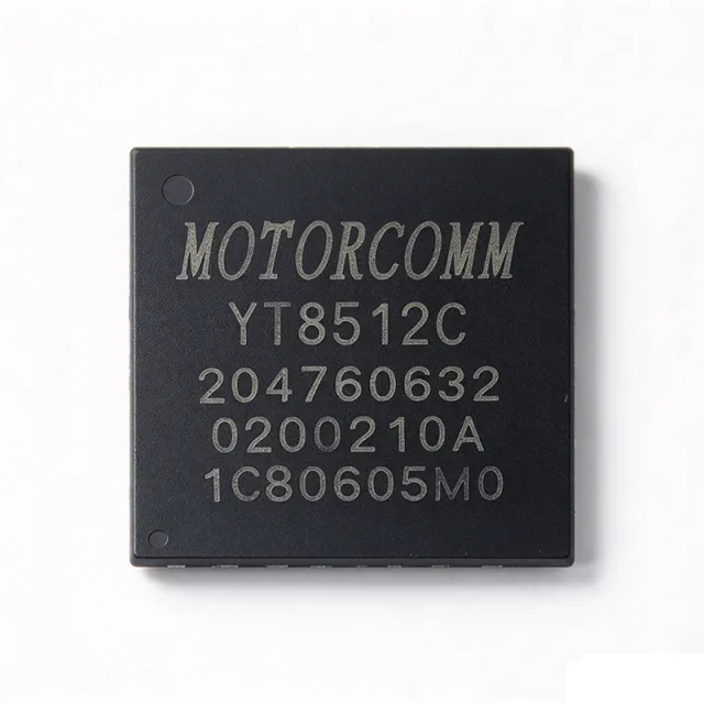
YT8512C - 10/100Mbps Ethernet PHY Transceiver, MII/RMII | Motorcomm
YT8512C

YT8512C - 10/100Mbps Ethernet PHY Transceiver, MII/RMII | Motorcomm

The Motorcomm YT8512C is a low-power single-port 10/100 Mbps Fast Ethernet PHY transceiver housed in a 32-pin QFN (5x5 mm) package. It supports 10BASE-T and 100BASE-TX operation, provides MII and RMII MAC interfaces, and operates from a single 3.3V supply with commercial-grade 0C to +70C temperature range. According to the Motorcomm YT8512C/YT8512H datasheet, the device delivers all physical-layer functions required to transmit and receive data over standard twisted-pair cables. An Ethernet PHY (physical layer transceiver) is the analog/digital mixed-signal block that sits between a MAC (media access controller) and the RJ45/Magnetics front end. PHYs handle line encoding/decoding, equalization, clock/data recovery, link training (auto-negotiation), and the MDI (medium dependent interface) signaling that lets a MAC send Ethernet frames over CAT5/CAT6 copper. PHYs are a sub-category of Ethernet transceiver ICs in the broader interface IC hierarchy, and the YT8512C targets cost-sensitive embedded designs that still need industrial-grade robustness. Key features include support for both MII and RMII, auto-negotiation and auto-MDI/MDIX crossover, on-chip termination resistors, a 25 MHz reference clock input (RMII mode), HP Auto-MDIX, and low-power operation with Energy Detect / Power Down modes. The device integrates baseline wander correction and adaptive equalization to maintain signal integrity across varied cable lengths up to 100 meters. Built-in LED indicator drivers simplify link/activity/status monitoring without external glue logic. Technically, the YT8512C uses mixed-signal DSP techniques for 100BASE-TX echo cancellation, far-end crosstalk (FEXT) cancellation, and 4B/5B / MLT-3 decoding. Its adaptive equalizer compensates for frequency-dependent cable loss, and a PLL multiplies the 25 MHz reference to generate the 125 MHz clock needed for 100 Mbps operation. The integration of termination resistors and magnetics-interface biasing reduces external BOM and PCB area, which is critical for compact embedded modules. Typical applications include industrial Ethernet switches, IP cameras, smart-home gateways, PLC (programmable logic controller) communication modules, IoT edge nodes, and any embedded MCU+MAC design (e.g., STM32 Ethernet, NXP i.MX RT, Linux SoMs) that needs a low-cost 10/100 Mbps copper interface. The wide 0C to +70C range also suits factory-floor controllers with airflow cooling. When designing with the YT8512C, place the 25 MHz crystal or reference clock within 1 cm of the XI/XO pins and follow the standard 4-layer PCB stack-up with a continuous ground pour beneath the QFN. Ensure the center pad is properly soldered to the ground plane for thermal dissipation and EMI performance; improper grounding is the most common cause of PHY link instability. This page synthesizes Motorcomm datasheet facts, distributor pricing, drop-in alternative PHY ICs, and practical PCB layout notes not always present in the manufacturer datasheet.

Permintaan RFG Kontak
Z84C4310AEG - Z80 SIO/3 10MHz CMOS Serial I/O | Zilog
Z84C4310AEG

Z84C4310AEG - Z80 SIO/3 10MHz CMOS Serial I/O | Zilog

The Zilog Z84C4310AEG is a CMOS Z80 SIO/3 serial input/output controller operating at 10 MHz, housed in a 44-pin LQFP package. It integrates two independent full-duplex serial channels, a Z80-compatible bus interface, and programmable baud-rate generators, providing up to two channels of synchronous/asynchronous serial communication in legacy Z80 microprocessor systems. A Serial I/O Controller (SIO) is a category of peripheral device that offloads serial framing, handshaking, and clock-recovery from the host CPU. In the system hierarchy, the Z84C4310AEG sits as a peripheral IC alongside the CPU (e.g., Z84C00 Z80), the CTC counter-timer, and the PIO parallel I/O. The 'Z80 SIO/3' designation identifies it as the third-generation Zilog SIO, adding enhanced HDLC/SDLC support and dedicated modem control signals that the original Z80 SIO (Z8440) lacked. Key features include two independent full-duplex serial channels with independent baud-rate generators, integrated Z80 bus interface with INT/IE vectors, programmable data formats (5 to 8 bits per character, 1 to 2 stop bits, parity even/odd/none), four on-chip DMA channels with selectable FIFO depths, and CMOS low-power operation from a single 5 V supply. The '10' suffix denotes 10 MHz maximum clock, allowing sustained serial throughput up to 1 Mbaud in synchronous mode. Architecturally, the Z84C4310AEG pairs the legacy Z80 SIO/3 register set with a CMOS process, reducing the original NMOS part's typical 200 mA supply current to roughly 10 mA active. Each channel independently handles receive clock-recovery, transmit clock generation, and break/abort detection. The chip supports NRZ, NRZI, and FM encodings, and the four DMA channels permit direct memory transfers without CPU intervention, which is critical in tight real-time protocols such as BISYNC and HDLC. Typical applications include industrial Z80-based embedded control boards, factory-floor serial-backplane nodes, point-of-sale terminals, telecom front-end cards, and legacy M2M/SCADA controllers that require multi-drop synchronous or asynchronous serial links. Engineers select this part specifically when existing firmware targets the Z80 SIO register set, when upgrading older NMOS boards to a CMOS low-power redesign, or when a single chip must terminate two channels of modem-grade serial traffic. Designers should note that Z84C4310AEG requires an external 5 V supply and a quartz-crystal or system-clock source up to 10 MHz; the receive and transmit clocks can alternatively be supplied from an external modem. Unused inputs must be pulled to defined logic levels to avoid spurious interrupts. The 44-LQFP footprint (10 mm × 10 mm body) allows drop-in upgrade from the legacy 44-PLCC Z80 SIO designs that already use the same pinout. This page synthesizes distributor pricing, drop-in alternatives, and practical design notes not found in the manufacturer datasheet alone, including cross-family same-brand variants and architectural context for engineers maintaining or upgrading legacy Z80 platforms.

Permintaan RFG Kontak
ZL88801LDF1 - Dual Ch FXS Wideband VoicePort 100V 64-QFN | Microchip
ZL88801LDF1

ZL88801LDF1 - Dual Ch FXS Wideband VoicePort 100V 64-QFN | Microchip

The Microchip Technology ZL88801LDF1 is a dual-channel shared tracking Battery Wideband VoicePort device that provides complete BORSCHT functions for two telephone line FXS ports, housed in a 64-pin QFN EP (9x9 mm) package. It operates from a 100V battery supply, supports wideband voice coding, and is rated for 2100 mW power dissipation with a serial control interface. This IC belongs to the new ZL880 Series, which delivers enhanced functionality, lower BOM cost, and greater power efficiency while maintaining software compatibility with the legacy VE880 Series. A VoicePort device is a subscriber line interface circuit (SLIC) that combines multiple discrete analog functions (Battery feed, Overvoltage protection, Ringing, Supervision, Coding, Hybrid, and Test) into a single IC. Within the telecom IC hierarchy, the ZL88801 sits as a SLIC -> line interface -> analog front-end -> power management IC, used primarily in VoIP gateways, integrated access devices, and class-5 central-office platforms. The wideband capability supports modern G.722 and Opus codecs by extending the audio passband beyond the 3.4 kHz limit of POTS telephony. Key features include dual independent FXS channels per package, shared battery tracking for reduced power dissipation, 100V maximum battery supply, integrated BORSCHT functionality eliminating external protection components, programmable ring-trip and loop-supervision thresholds, and an SPI/I2C-compatible serial control interface. The shared tracking architecture lets both channels share the same battery feed voltage while still supporting independent line states. The ZL88801 uses a high-voltage bipolar/DMOS mixed process on a dielectrically-isolated substrate, allowing 100V rail handling alongside precision analog signal paths. Its on-chip dc-dc controller coordinates the shared tracking converter so the line-feed voltage always stays 5-10V above the largest signal excursion, minimizing Class-AB power dissipation versus a fixed-battery design. Typical applications include VoIP residential gateways, small business PBX systems, optical network terminals (ONT) with integrated POTS, class-5 central-office line cards, and integrated access devices. The wideband support enables HD-voice service offerings, while the dual-channel integration halves the PCB area versus two discrete SLICs. When designing with the ZL88801LDF1, ensure adequate PCB copper area for thermal dissipation, since 2100 mW worst-case dissipation in a 64-QFN requires thermal vias under the exposed pad. Always program the ring-trip and off-hook thresholds is configurable. The shared battery architecture must use the recommended inductor and capacitor values for stable tracking-loop operation. This page synthesizes distributor pricing, drop-in same-family alternatives, and practical thermal/design notes not consolidated on the manufacturer product page.

Permintaan RFG Kontak
ZSSC4151AE2R - Automotive Resistive SSC | 24-QFN | Renesas
ZSSC4151AE2R

ZSSC4151AE2R - Automotive Resistive SSC | 24-QFN | Renesas

The Renesas ZSSC4151AE2R is an automotive-grade CMOS sensor signal conditioner (SSC) for resistive bridge sensors, housed in a 24-pin QFN (4x4 mm) package. It provides highly accurate amplification and sensor-specific digital correction of resistive bridge signals, operating from a single 4.5 V to 5.5 V analog supply with analog ratiometric output. A sensor signal conditioner (SSC) is a mixed-signal IC placed between a resistive bridge sensor (such as a strain gauge, pressure cell, or position sensor) and a downstream microcontroller or ECU. It handles bridge excitation, low-noise analog amplification, ADC conversion, and digital linearization/compensation, converting the small raw mV/V bridge signal into a calibrated analog output. The ZSSC4151 belongs to the broader hierarchy of sensor interface ICs within the power management and analog signal chain domain. Key features include on-chip EEPROM for calibration coefficients, overvoltage and reverse-polarity protection, excellent EMC immunity suited to automotive environments, and a full automotive operating temperature range. Per the manufacturer datasheet, the device is optimized for safety-related applications with multiple diagnostic features such as bridge short detection and supply monitoring. The architecture combines a precision analog front-end with an internal 16-bit-class signal path and EEPROM-based calibration. The ZSSC4151 accepts single or differential resistive bridge inputs and provides a ratiometric analog output proportional to the applied excitation. Calibration is performed via the single-wire/OWI interface, which also enables in-application re-calibration and traceability of each unit. Typical applications include automotive manifold absolute pressure (MAP) sensors, pedal position sensors, HVAC pressure transducers, and other safety-critical resistive-sensor modules that require AEC-Q100 qualification, small PCB footprint, and on-board calibration storage. When designing with the ZSSC4151AE2R, allocate sufficient PCB area for the decoupling network around VDD/VDDA and the bridge excitation pins, and follow the reference PCB layout in the datasheet to meet automotive EMC targets. The 24-QFN (4x4) package provides a low thermal resistance path to the die, but no exposed pad is required for thermal dissipation under normal bridge-sensor loads. This page synthesizes distributor pricing, drop-in alternatives, and practical design notes not found in the manufacturer datasheet.

Permintaan RFG Kontak
ZZISO-20260819 - High-Speed Isolated Digital Isolator | XAIPART
ZZISO-20260819

ZZISO-20260819 - High-Speed Isolated Digital Isolator | XAIPART

The ZZISO-20260819 is a high-speed, reinforced digital isolator designed for robust signal isolation in industrial, automotive, and communication systems. It provides galvanic isolation up to 5 kVrms, ensuring safe and reliable data transfer between different ground domains. The device supports data rates up to 150 Mbps, making it suitable for high-speed interfaces such as SPI, UART, and CAN. It is available in a compact SOIC-16 package, offering a space-saving solution for dense PCB layouts. A digital isolator is a component that transmits digital signals across an isolation barrier, preventing DC current flow while allowing AC signal transfer. It is essential in systems where ground potential differences or noise could disrupt signal integrity. Digital isolators are part of the broader category of isolation components, which also includes optocouplers and magnetic isolators. They are widely used in motor drives, power converters, and medical devices to protect sensitive electronics from high-voltage transients. Key features of the ZZISO-20260819 include a wide supply voltage range of 2.5V to 5.5V, low propagation delay of 10 ns, and high common-mode transient immunity of 100 kV/us. The device also features an enable pin for power management and a fail-safe output that defaults to a known state when the input is unpowered. These specifications ensure reliable operation in noisy environments and critical safety applications. Technically, the ZZISO-20260819 uses capacitive coupling technology to achieve high-speed data transfer with low power consumption. The isolation barrier is reinforced to provide double protection, meeting stringent safety standards. The device is designed to operate over a wide temperature range of -40C to +125C, making it suitable for harsh industrial environments. Its low quiescent current of 1.5 mA per channel helps reduce overall system power consumption. Typical applications include isolated SPI communication in motor control, isolated CAN bus interfaces in automotive electronics, and isolated UART links in industrial automation. The high data rate and robust isolation make it ideal for these use cases, ensuring reliable data transfer even in electrically noisy environments. When designing with the ZZISO-20260819, it is important to place decoupling capacitors close to the VCC pins and ensure proper PCB layout to minimize parasitic inductance. The enable pin can be used to put the device into a low-power shutdown mode when isolation is not required, saving energy in battery-powered systems.

Permintaan RFG Kontak