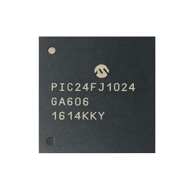
PIC24FJ128DA106T-I/MR
PIC24FJ128DA106T-I/MR - 16-bit 32MHz 128KB Flash MCU | Microchip
The Microchip Technology PIC24FJ128DA106T-I/MR is a 16-bit PIC microcontroller from the PIC24F-DA family, operating at up to 32 MHz and integrating 128 KB of FLASH program memory organized as 43K x 24, plus 24 KB of RAM. Housed in a 64-pin VQFN (9x9 mm, MR) package with exposed thermal pad, it combines a high-throughput PIC core with on-chip USB OTG, a graphics display controller, and a dedicated graphics accelerator capable of directly driving displays up to 4.3" WQVGA at 480 x 272 resolution. The integrated peripherals include I2C, IrDA, SPI, UART/USART, and USB OTG, making the part a single-chip solution for human-machine interface (HMI) and embedded graphical applications.
A 16-bit microcontroller (MCU) is a microprocessor that fetches, decodes, and executes 16-bit instructions in a single cycle, offering higher code density and arithmetic precision than 8-bit cores while remaining easier to program than 32-bit ARM Cortex devices. In the broader taxonomy, the PIC24FJ128DA106 belongs to the 16-bit MCU class -> general-purpose microcontroller -> embedded microcontroller -> integrated circuit. The 'DA' suffix denotes the graphics-controller sub-family within Microchip's PIC24F line, which targets cost-sensitive graphical UI designs that previously needed an external LCD controller.
Key features of this device include its 32 MHz core with 16 MIPS throughput, hardware USB 2.0 full-speed On-The-Go with physical-layer transceiver, an integrated 480 x 272 capable display controller, parallel master port (PMP) for direct bus attachment to LCD panels, and multiple connectivity peripherals (UART, SPI, I2C, IrDA). It also provides up to 53 general-purpose I/O pins and several 16-bit timers suitable for RTOS-based designs. The wide operating voltage range and rich peripheral set allow the same silicon to span consumer, industrial, and battery-powered HMI products.
The PIC24FJ128DA106 architecture uses a 16-bit modified Harvard core with hardware multiply, hardware divide, and a 16 x 16-bit working register array. The display pipeline offloads pixel blitting and font rendering from the CPU, leaving MIPS budget for application logic and communication stacks. Internal Phase-Locked Loop (PLL) synthesizes the 32 MHz system clock from the on-chip 8 MHz oscillator, and a real-time clock calendar (RTCC) module supports timekeeping during low-power modes.
Typical applications include handheld medical-device HMIs, industrial control panels with TFT displays, USB-equipped data loggers, smart-home thermostats with color LCD, and portable instrumentation. The combination of native USB, graphics acceleration, and 128 KB FLASH lets designers ship a full graphical UI plus USB stack on a single chip.
When designing with this part, allocate sufficient PCB area for the 9 x 9 mm VQFN exposed pad, which must be soldered to a continuous copper plane for both thermal dissipation and ground integrity. Decouple VDD/VUSB with 100 nF + 4.7 uF capacitors placed within 5 mm of each supply pin, and follow Microchip application note AN1367 for the USB-OTG board layout checklist.
This page synthesizes distributor pricing, same-package drop-in alternatives, and practical design notes not found in the manufacturer datasheet alone, giving procurement and design engineers a consolidated view of the part for engineering decisions.
見積もり
お問い合わせ