製品 (39,000+)

IT6263FN/BX - De-SSC LVDS-to-HDMI Converter QFN-64 | ITE
IT6263FN/BX

IT6263FN/BX - De-SSC LVDS-to-HDMI Converter QFN-64 | ITE

The ITE IT6263FN/BX is a high-performance single-chip De-SSC (De-Spread Spectrum Clocking) LVDS-to-HDMI converter that integrates an LVDS receiver and an HDMI 1.4a transmitter in one package, providing conversion from LVDS input to HDMI 1.4 output. It supports LVDS input clock rates up to 150 MHz, input color depth up to 10-bit, and output deep-color depth up to 12-bit. The device complies with HDMI 1.3, HDMI 1.4a, HDCP 1.2, and DVI 1.0, and accepts single-link or dual-link LVDS data mappings including Open LDI, JEIDA, and VESA formats. A De-SSC LVDS-to-HDMI converter is a specialized bridge IC used in display applications where the source uses an LVDS interface with intentional spread-spectrum clock modulation (used to reduce EMI), but the downstream display only accepts clean HDMI. The IC sits between an LVDS panel-timing generator (SoC, GPU, or media processor) and the HDMI connector, and must transparently remove the SSC modulation so that downstream HDMI timing budgets remain valid. The broader hierarchy is: display bridge converter -> LVDS-to-HDMI bridge -> interface converter -> signal conditioner IC -> semiconductor. Key features include on-chip De-SSC processing (a different value from raw LVDS-to-HDMI bridges such as the IT6261), integrated HDCP 1.2 cipher engine with on-chip keys, dual-link LVDS receiver supporting up to 1920x1200, and an HDMI 1.4a transmitter capable of 1080p60 with 3D-frame-packing support. The part also provides I2C slave control, configurable color mapping, and integrated termination resistors, reducing external component count. The IT6263FN/BX is built on a CMOS mixed-signal process and uses an internal PLL to recover pixel clock and regenerate a clean HDMI TMDS link. Its embedded HDCP hardware engine authenticates the sink device and encrypts the AV stream, making the IC suitable for protected content paths. Internal configurable registers exposed through I2C allow fine-tuning of swing, pre-emphasis, color-depth, and mapping selection. Typical applications include automotive head-unit HDMI outputs from LVDS-SoCs, set-top boxes that repurpose LVDS panels with HDMI repeaters, pico-projectors and LED-projector HDMI bridges, embedded HDMI dongles next to industrial panel controllers, motherboards that need LVDS-to-HDMI for external displays, and digital signage players that interface LVDS media SoCs to HDMI panels. When designing with this part, ensure the LVDS traces are length-matched within the differential-pair tolerance in the datasheet, place a 100 nF decoupling capacitor close to each DVDD pin, and route HDMI TMDS pairs with controlled 100-ohm differential impedance. The embedded HDCP keys require a signed licence from ITE for licensing-protected production runs. This page synthesises distributor pricing, drop-in alternatives, and practical design notes that go beyond the manufacturer datasheet summary.

見積もり お問い合わせ
ITJKK - 1Mbaud CAN Transceiver | Infineon Technologies
ITJKK

ITJKK - 1Mbaud CAN Transceiver | Infineon Technologies

Infineon Technologies ITJKK is a 1Mbaud CAN transceiver orderable as TLE6250G ITJKK in an 8-SOIC package. The device provides one CAN driver and one receiver, operates from a 4.5V to 5.5V supply, and is supplied in tape-and-reel packaging. It is identified as an automotive AEC-Q100-qualified, 5V standby-capable CAN interface for robust automotive and industrial networks. A CAN transceiver is an interface IC that connects a host controller's digital logic to a physical CAN bus. In the hierarchy, a CAN transceiver is a bus transceiver, an interface transceiver, an interface IC, and ultimately a semiconductor. Its driver converts controller signals into the electrical levels required on the bus, while its receiver converts bus signals back into logic-compatible information for the controller. The ITJKK order code identifies a single-driver, single-receiver device with 1Mbaud CAN operation. Its 4.5V to 5.5V supply range supports regulated 5V systems, and the 8-SOIC package provides a surface-mount footprint for automotive and industrial control equipment. Tape-and-reel packaging is suitable for automated PCB assembly and volume manufacturing. The verified product information identifies this device as an automotive CAN-bus transceiver associated with AEC-Q100 qualification. This makes the ITJKK relevant to applications requiring a dedicated CAN physical layer, including vehicle body controllers, electronic control units, industrial automation equipment, and embedded diagnostic systems. The 1Mbaud rating supports communication rates up to 1Mbaud when used within the complete bus system's timing, termination, and fault-tolerance requirements. Designers should not treat transceiver bandwidth as the only CAN system criterion. Bus length, topology, termination, propagation delay, logic levels, electromagnetic compatibility, fault behavior, and the selected microcontroller or CAN controller must also be evaluated. The 8-SOIC footprint must be matched exactly when replacing a PCB design, and any candidate substitute must be checked for pin compatibility, supply range, standby behavior, thermal rating, and qualification status. The principal sourcing advantage is the clearly identified Infineon Technologies order code and the availability information reported by multiple distributors. However, the supplied results do not provide a current unit-price schedule, a complete pin table, or verified cross-brand drop-in equivalents. Engineers should therefore verify current pricing, lead time, lifecycle status, pinout, and qualification documentation before releasing a production BOM. This page combines the verified distributor specifications, package information, procurement context, and replacement limitations for the ITJKK order code. It also distinguishes documented facts from parameters that require confirmation from the manufacturer datasheet, helping engineering teams assess this CAN transceiver without assuming that a similar-package device is automatically a safe drop-in replacement.

見積もり お問い合わせ
J3455E - Intel Celeron Quad-Core SoC 2.3 GHz 10W Embedded | Intel
J3455E

J3455E - Intel Celeron Quad-Core SoC 2.3 GHz 10W Embedded | Intel

The Intel Celeron J3455E is a quad-core embedded System-on-Chip (SoC) from the Apollo Lake family, featuring 4 cores/4 threads, a 2 MB L2 cache, and a base frequency of 1.50 GHz that bursts up to 2.30 GHz. It integrates Intel HD Graphics 500 with 12 execution units and is manufactured on Intel's 14 nm process with a 10 W TDP, targeting embedded and low-power applications. The term SoC (System-on-Chip) refers to a single silicon die that integrates the CPU cores, GPU, memory controller, and platform I/O (PCIe, SATA, USB) into one package. Apollo Lake SoCs like the J3455E belong to the Atom/Celeron/Pentium Silver hierarchy, which itself sits within Intel's broader embedded and entry-level desktop x86 product stack. By collapsing chipset functions into the same package, Apollo Lake platforms reduce board area, BOM cost, and power envelope compared to discrete CPU-plus-chipset designs of prior generations. Key features of the J3455E include 4 physical cores without Hyper-Threading, a 2 MB shared L2 cache, dual-channel DDR3L/LPDDR3 up to 1866 MT/s and LPDDR4 up to 2400 MT/s memory support, and Intel HD Graphics 500 running up to 750 MHz. I/O includes PCIe 2.0 lanes, SATA 3.0, USB 3.0, and integrated audio. The 10 W scenario design power enables fanless thermal designs, while the 14 nm lithography keeps leakage low for always-on embedded workloads. Architecturally, the J3455E uses Intel's Goldmont CPU microarchitecture, which delivers significantly higher IPC than the prior Braswell/Airmont generation while maintaining the same low-TDP envelope. The integrated HD Graphics 500 (Gen9 LP architecture) supports hardware-accelerated decode for H.265/HEVC and VP9, making the part suitable for digital signage and media playback. The SoC is firmware-configurable for either 6 W or 10 W TDP modes, letting OEMs trade sustained performance against power budget. Typical applications for the J3455E include digital signage players, thin-client terminals, entry-level POS systems, industrial HMI panels, retail kiosks, and fanless embedded boxes. Its low TDP and integrated I/O make it a strong fit where a full desktop CPU is over-spec but ARM-based SoCs lack x86 software compatibility. The part's 10-year embedded lifecycle support also suits long-life industrial designs. When designing with the J3455E, ensure the carrier board implements both PCIe x1 and x2 reference clock routing per Intel's Apollo Lake Platform Design Guide, and use wide copper pours under the SoC package to spread the 10 W dissipation across the PCB. For thermal margin in sealed enclosures, derate the TDP to 6 W via the platform firmware if the chassis cannot sustain 10 W continuously. This page consolidates distributor pricing, embedded lifecycle context, drop-in alternatives, and design notes that supplement the official Intel product page and datasheet references.

見積もり お問い合わせ
JHL7440 - Intel Thunderbolt 3 Controller | BGA-337
JHL7440

JHL7440 - Intel Thunderbolt 3 Controller | BGA-337

The Intel JHL7440 (also sold as JHL7440 S LMJ2 / JHL7440 S LMHZ) is an Alpine Ridge-based Thunderbolt 3 controller IC that integrates USB 3.1, DisplayPort 1.4, and Thunderbolt 3 (40 Gbps) into a single BGA package, providing four lanes of PCIe 3.0 tunneling and dual-protocol downstream connectivity for docks, NVMe enclosures, and host platforms. A Thunderbolt controller is a high-speed protocol bridge IC that aggregates multiple serial bus standards (PCI Express, USB, DisplayPort) onto a unified 40 Gbps Thunderbolt cable/connector while providing power negotiation via USB Power Delivery. It sits between the platform's internal PCIe/USB/DP lanes and the external USB-C port, enabling a single-cable docking station, eGPU, or NVMe enclosure solution. The JHL7440 belongs to Intel's Falcon Ridge / Alpine Ridge generation and is widely used in add-in cards, NVMe SSD enclosures, and second-generation Thunderbolt 3 docks. Key features of the JHL7440 include: Thunderbolt 3 at 40 Gbps bidirectional bandwidth (4 lanes of PCIe 3.0 bi-directional), native DisplayPort 1.4 with HBR3 support (8.1 Gbps per lane, 32.4 Gbps aggregate for dual-display 8K), USB 3.1 Gen 2 (10 Gbps) backward compatibility, USB Power Delivery 3.0 support up to 100 W downstream, integrated PCIe 3.0 switch with 4 downstream ports, and HDCP 2.2 content protection. The controller targets host platforms that lack native TB3 support and is most commonly deployed on M.2/NGFF key-M add-in cards (TB3 AIC) that plug into a motherboard's PCIe 3.0 x4 slot. Architecturally, the JHL7440 combines a Thunderbolt PHY, a PCIe 3.0 controller, a USB 3.1 controller, a DisplayPort 1.4 receiver/transmitter, a USB-PD 3.0 controller, and an embedded microcontroller into a single 14 x 14 x 1.4 mm BGA-337 package with 0.65 mm pitch. Power consumption is rated at approximately 3.0 W typical / 4.5 W peak, requiring active cooling (heatsink and airflow) for sustained throughput — a common design constraint in NVMe enclosures that must merge TB3 + 10 Gb/s NVMe heat into a small footprint. Typical applications for the JHL7440 include Thunderbolt 3 add-in cards and M.2 NVMe SSD enclosures (40 Gbps), Thunderbolt 3 docking stations with dual 4K or single 8K DisplayPort 1.4 outputs, eGPU enclosures that tunnel x4 PCIe 3.0 to an external graphics card, USB-C port expanders providing downstream USB 3.1 Gen 2 and DP-alt mode, and broadcast / video editing rigs that need high-bandwidth storage bridges. Pin compatibility with JHL6340 (previous-gen) allows retrofit of older TB3 cards after firmware validation. When designing with the JHL7440, allocate a thermal solution capable of dissipating 4.5 W peak — passive heatsinks are marginal in enclosed NVMe enclosures, so forced airflow or a thermally-bonded aluminum chassis is recommended for production designs. Verify firmware/BIOS support on legacy motherboards that lack native Alpine Ridge platform support.

見積もり お問い合わせ
JHL7440-S-LMHZ - Thunderbolt 3 Controller, Dual Port BGA | Intel
JHL7440-S-LMHZ

JHL7440-S-LMHZ - Thunderbolt 3 Controller, Dual Port BGA | Intel

The Intel JHL7440-S-LMHZ is a second-generation Thunderbolt 3 controller IC housed in a 337-ball BGA package (FC-CSP, 10.7 x 10.7 mm). It is a Dual Port Device variant from the JHL7440 series, providing two Thunderbolt 3 ports operating at up to 40 Gbps bi-directional bandwidth, with native support for USB 3.1 Gen 2, DisplayPort 1.4, and PCIe 3.0 tunneling. The -LMHZ ordering code designates the specific package, temperature grade, and lead-free / RoHS-compliant configuration used in production designs. A Thunderbolt 3 controller is a high-speed protocol-aggregating interface IC that consolidates multiple peripheral buses (PCI Express, DisplayPort, USB) into a single USB-C cable carrying up to 40 Gbps of combined traffic. Controllers such as the JHL7440 sit between a host system's PCIe/DisplayPort/USB controllers and an external Type-C connector, performing protocol multiplexing, link training, power delivery negotiation (USB PD), and tunneled-stream management. The JHL7440 specifically implements Alpine Ridge-generation features including DP 1.4 alt-mode and USB PD 3.0, and in the Dual Port configuration can drive two Thunderbolt 3 ports from a single chip. Key distinguishing features of the JHL7440-S-LMHZ include 40 Gbps Thunderbolt 3 line rate per port, integrated DisplayPort 1.4 receiver capable of 8K HDR outputs via HBR3 (8.1 Gbps per lane, 32.4 Gbps aggregated), PCIe 3.0 x4 host upstream interface, USB 3.1 Gen 2 (10 Gbps) downstream support, and integrated USB Power Delivery 3.0 controller. The 337-ball FC-CSP package utilizes an exposed-die land-grid array for the shortest possible signal paths to the high-speed SerDes, which is essential for multi-Gbps link training. Typical applications include Thunderbolt 3 docking stations, NVMe SSD enclosures that saturate 40 Gbps pipes, 8K DisplayPort adapters and video capture cards, high-end workstation motherboards, and eGPU enclosures. The Dual Port configuration is especially popular in docking stations where one port connects to a host laptop and the other to downstream peripherals. When designing with the JHL7440, PCB layout must allocate separate reference-clock domains, keep the high-speed TX/RX pairs length-matched within sub-millimeter tolerances, and provide a clean PCIe 3.0 host connection - any signal-integrity issue at 10+ Gbps will surface as Thunderbolt link-training failures. This page synthesizes verified distributor pricing, drop-in alternatives, and practical Thunderbolt 3 design considerations not found in any single distributor catalog.

見積もり お問い合わせ
JHL7440-S-LMJ2 - Intel Titan Ridge Thunderbolt 3 Controller | BGA-337
JHL7440-S-LMJ2

JHL7440-S-LMJ2 - Intel Titan Ridge Thunderbolt 3 Controller | BGA-337

The Intel JHL7440-S-LMJ2 is the Intel "Titan Ridge" Thunderbolt 3 (Alpine Ridge successor) controller IC, an I/O controller delivered in a 10.7 mm x 10.7 mm BGA-337 package. It implements the Thunderbolt 3 protocol on four PCIe 3.0 lanes and downstream DisplayPort 1.4 muxing, supporting dual 4K@60 Hz DisplayPort 1.4 outputs or one 5K@60 Hz output when paired with an Alpine Ridge-compatible host. The JHL7440 is a peripheral/device-side (LMJ2 suffix denotes the device-mode SKU) Thunderbolt 3 controller commonly used in NVMe SSD enclosures, Thunderbolt 3 docks, and external graphics (eGPU) chassis. A Thunderbolt 3 controller is a high-speed protocol bridge that aggregates PCIe 3.0, DisplayPort 1.2/1.4, and USB 3.1 Gen 2 traffic onto a single Type-C connector using the Thunderbolt 3 alternate-mode physical layer. The JHL7440 belongs to Intel's Titan Ridge (JHL7x40) family, which succeeded the Alpine Ridge (JHL6x40) family and pre-dated the Goshen Ridge (JHL8x40) and Barlow Ridge (JHL9580) controllers. In the wider taxonomy: Thunderbolt controller -> I/O controller -> interface IC -> semiconductor. The "Thunderbolt" word-mark is an Intel-registered protocol distinct from USB4 in its early implementations, although USB4 incorporates the Thunderbolt 3 protocol layer. Key features include 40 Gbps aggregate bi-directional bandwidth (Thunderbolt 3 mode), backward compatibility with Thunderbolt 1/2 over active cables, native USB 3.1 Gen 2 (10 Gbps) support on the Type-C ports, and DisplayPort 1.4 muxing with HDR/REC.2020 support. The device-mode (LMJ2) variant disables the upstream host port and adds a downstream PCIe-only orientation, making it ideal for compact NVMe enclosures where one Type-C port connects to the host and an internal PCIe 3.0 x4 link connects to the NVMe SSD. Firmware is loaded from external SPI flash. In typical applications, the JHL7440-S-LMJ2 sits between an M.2 NVMe SSD (PCIe 3.0 x4) and a Thunderbolt 3 Type-C connector, providing up to ~2.8 GB/s real-world transfer speeds. It is also used in Thunderbolt 3 docks where it functions as a downstream port multiplier connecting to USB 3.1 Gen 2 hubs, SATA controllers, GbE controllers, and audio codecs over PCIe. External GPU enclosures used this controller in early designs before the eGPU market consolidated around Thunderbolt 4 and OCuLink. Designers must route 85-ohm differential pairs for the four PCIe 3.0 TX/RX lanes and the high-speed Thunderbolt SERDES links; the part requires a low-jitter reference clock and a USB Type-C port controller (often a TUSB8041 or discrete CC-logic) to negotiate Thunderbolt mode. Firmware recovery and reflash should be exposed via a vendor-specific procedure because the device-mode SKU will not enumerate as a Thunderbolt host upstream.

見積もり お問い合わせ
JHL7540 - 40 Gbps Thunderbolt 3 Controller | Intel
JHL7540

JHL7540 - 40 Gbps Thunderbolt 3 Controller | Intel

The Intel JHL7540 is a Thunderbolt 3 controller and USB-C interface IC providing 40 Gbps bidirectional bandwidth in the host-controller role. Verified listings identify the device as a dual-port controller and place it in a 10.7 mm × 10.7 mm FC-CSP BGA package, with JHL7540 S LMHR shown as the tray ordering variant. Its core function is to interface a host system with Thunderbolt 3 and USB-C connections while coordinating high-speed data transfer, power-oriented USB-C behavior, and platform connectivity. A Thunderbolt controller is an interface semiconductor that bridges a computer or embedded platform with Thunderbolt-compatible peripherals. Within the connectivity hierarchy, Thunderbolt 3 uses the physical and protocol capabilities associated with 40 Gbps-class links, while USB-C provides the physical connector used by compatible systems. The JHL7540 is consequently more specialized than a general USB interface controller and is intended for designs requiring the verified Thunderbolt 3 host-controller role. Verified product information identifies USB as the interface type, an I/O-controller classification, dual-port operation, a maximum operating temperature of +65 C, and a minimum operating temperature of 0 C. The package is reported as 10.7 mm × 10.7 mm and supplied in a tray for the JHL7540 S LMHR variant. Other electrical details, including voltage ratings, power consumption, lane configuration details, firmware requirements, and exact electrical limits, are not supplied in the verified web data and should not be inferred. Typical implementation contexts include Thunderbolt 3 host systems, USB-C docking products, high-speed storage peripherals, external display or docking ecosystems, and embedded computing platforms that expose Thunderbolt connectivity. System designers must confirm host-platform support, connector routing, firmware compatibility, signal-integrity requirements, power delivery, and thermal conditions with Intel documentation before releasing a production design. The most important design consideration is that a controller MPN alone does not establish complete Thunderbolt interoperability. The board must implement the required USB-C and Thunderbolt routing, power-management behavior, firmware, connector configuration, and platform interoperability requirements. The verified package information should also be checked against the exact ordering suffix before placing an order. This page consolidates the verified distributor and distributor-indexed product information, while clearly separating missing technical data from confirmed facts. It is intended to support initial sourcing and engineering triage for JHL7540-based Thunderbolt 3 designs.

見積もり お問い合わせ
JHL7540-S-LMHR - Dual-Port Thunderbolt 3 Controller | Intel
JHL7540-S-LMHR

JHL7540-S-LMHR - Dual-Port Thunderbolt 3 Controller | Intel

The Intel JHL7540-S-LMHR is a dual-port host controller for Thunderbolt 3 connectivity, supplied as the S-LMHR ordering variant in a 337-ball FC-CSP package measuring 10.7 mm by 10.7 mm. Verified listings identify the component as an I/O controller interface IC and Thunderbolt 3 controller, but the supplied sources do not publish a complete electrical parameter table. Consequently, unverified values such as supply voltage, lane count, power consumption, operating temperature, and maximum data rate are not asserted here. A Thunderbolt 3 host controller is a system-level I/O interface semiconductor that coordinates a computer or platform with Thunderbolt-compatible peripherals. It belongs to the I/O controller class, within interface ICs and semiconductors. Thunderbolt technology combines high-bandwidth data transfer, display connectivity, and power delivery over a physical connection, while the controller supplies the platform-facing logic required to manage those functions. The JHL7540 is particularly relevant to desktop, workstation, and embedded Thunderbolt-capable platforms. The verified JHL7540-S-LMHR ordering information establishes dual-port host functionality, Thunderbolt 3 controller classification, FC-CSP construction, tray packaging, and a 10.7 mm by 10.7 mm package. The suffix “S-LMHR” identifies the specific orderable configuration, but its decode and environmental qualifiers are not present in the supplied evidence and should not be inferred. Intel support and specifications pages provide authoritative sources for architecture, platform support, and lifecycle information, while distributor records provide sourcing and package details. Because this controller supports a differential, high-speed interface, PCB design must prioritize short matched routes, continuous reference planes, controlled impedance, and careful connector-to-controller escape routing. BGA assembly also requires stencil, reflow-profile, pad-array, and solder-joint validation appropriate to the manufacturer’s package documentation. Exact layer count, ball-map details, and assembly process requirements must be obtained from the official package drawing before layout release. Potential uses include Thunderbolt expansion chassis, high-resolution external-display systems, professional storage arrays, multi-display workstations, capture systems, and compact desktop platforms. Selection should begin with the host platform’s supported controller generation, firmware support, connector requirements, and Intel platform validation. A different Thunderbolt controller should not be substituted solely because its bandwidth appears similar; electrical, pin, firmware, and platform compatibility must be demonstrated first. This page distinguishes verified ordering and product facts from unknown technical fields instead of filling gaps with assumptions. It also combines the supplied distributor evidence, Intel product resources, and a strict review of available cross-reference results. No pin-compatible replacement was established from the provided data, so any alternative MPN would be misleading until its footprint, pinout, electrical limits, firmware support, and platform behavior are independently verified. The practical sourcing position is straightforward: confirm the Intel documentation revision and platform support, validate the complete 337-ball pin map and FC-CSP land pattern, and compare lead time against the production schedule before committing volume. The known tray package also requires procurement attention because large BGA components can be sensitive to moisture handling, solder-ball condition, and shipping exposure. Engineering release should include distributor traceability, assembly-yield testing, and firmware interoperability checks.

見積もり お問い合わせ
JHL7540-S-LMHS - Dual-Port Thunderbolt 3 Controller | Intel
JHL7540-S-LMHS

JHL7540-S-LMHS - Dual-Port Thunderbolt 3 Controller | Intel

The Intel JHL7540-S-LMHS is a dual-port host Thunderbolt 3 controller packaged as a 10.7 mm by 10.7 mm FC-CSP and supplied on tape and reel. Its verified source identifies it as Intel's Thunderbolt 3 controller for dual-port host implementations, placing it in the high-speed I/O controller and interface-controller hierarchy. An I/O controller interface IC coordinates communication between a host computing platform and external peripherals. A Thunderbolt 3 controller is a specialized high-speed interface controller that manages Thunderbolt links, connects compatible storage, displays, docks, and other peripherals, and supports the ecosystem of PCI Express and display-oriented connectivity associated with Thunderbolt 3. The exact electrical ratings beyond the verified identity and package information are not supplied in the source data and must be confirmed in Intel's product documentation before design release. The key verified features are dual-port host support, Thunderbolt 3 controller function, FC-CSP construction, a 10.7 mm by 10.7 mm package outline, and tape-and-reel packaging. The LMHS ordering suffix distinguishes the offered supply configuration from the separately listed LMHR tray option. Those suffixes are packaging and ordering identifiers, not evidence of a different controller function. Technically, the JHL7540 belongs in a platform-specific high-speed I/O design rather than a generic serial-interface application. Its implementation role is to provide the controller silicon required by a Thunderbolt-capable host system, while board designers must address power sequencing, high-speed routing, connector requirements, firmware support, and thermal management around the CSP package. The source data does not provide operating voltage, power consumption, signaling rates, temperature limits, pin names, or electrical timing values. Typical uses include Thunderbolt docks, external high-speed storage, workstation connectivity, laptop or desktop platform designs, and other systems requiring dual-port Thunderbolt 3 host connectivity. Suitability depends on validating the associated platform firmware, board layout, power delivery, connector design, and supported operating conditions rather than relying on the distributor category label alone. For a new layout, obtain the official package drawing and pin definitions, confirm the exposed-pad and ball requirements, and route high-speed differential signals as a controlled-impedance interconnect. Treat JHL7540-S-LMHS and JHL7540-S-LMHR as distinct ordering options until the manufacturer's orderable-parts information confirms whether their technical die and package treatment are identical. This page summarizes the verified manufacturer and distributor identity, records unavailable technical fields explicitly, and avoids inventing specifications that were not present in the supplied data. It is intended as an engineering starting point for sourcing and design validation, not as a substitute for Intel's complete controller documentation.

見積もり お問い合わせ
JHL8440 - Thunderbolt 4 Controller | Intel
JHL8440

JHL8440 - Thunderbolt 4 Controller | Intel

Intel JHL8440 is a Thunderbolt 4 controller designed for systems requiring high-speed USB4 and Thunderbolt connectivity. The supplied verified data identifies it as a quad-port device in an FC-CSP package, but it does not provide the full electrical, thermal, pinout, or pricing specifications needed for a complete engineering characterization. The available distributor listing describes JHL8440 as an Intel I/O controller interface IC and Thunderbolt 4 controller, while the manufacturer specifications page identifies the same device family. Engineers should use the exact package variant ordering code and the official Intel datasheet before committing a PCB layout or production BOM. A Thunderbolt controller is a high-speed interface IC that coordinates protocol translation, host or device connectivity, DisplayPort integration, and USB4 traffic. In the system hierarchy, it belongs to interface controllers, data-processing semiconductors, and computer connectivity solutions. Thunderbolt 4 builds on the 40 Gbps-class connectivity positioning described in the verified comparison material, but the supplied JHL8440 records do not establish lane count, maximum data rate, power delivery, DisplayPort configuration, host-versus-device operation, supported operating temperature, or power-consumption values. The verified distributor record gives the commercial identifier “JHL8440 S LN6U” and describes an FC-CSP tray package. Another search result identifies the “JHL8440 S LN6V” designation, but the supplied data does not establish whether these ordering codes differ only in packaging, shipment form, or another ordering attribute. Do not treat them as interchangeable without Intel documentation or an authorized distributor’s package cross-reference. The supplied comparison source also mentions RTS5490, JHL7440, JHL7540, and JHL8440 as 40 Gbps-class devices, but it specifically distinguishes RTS5490 as a USB4 hub controller and does not prove drop-in equivalence. Typical system uses for a device in this class include USB4 and Thunderbolt docks, laptop and desktop platform controllers, high-bandwidth storage, external display systems, and compact multiport accessories. These applications are engineering-context suggestions rather than verified Intel reference designs for JHL8440. A production design must confirm signal integrity, power sequencing, firmware support, connector requirements, and thermal performance against the official Intel documentation. This page consolidates the verified manufacturer and distributor references while explicitly marking unspecified technical data as unavailable.

見積もり お問い合わせ
JHL8440-S-LN6U - Thunderbolt 4 Quad Port Controller | Intel
JHL8440-S-LN6U

JHL8440-S-LN6U - Thunderbolt 4 Quad Port Controller | Intel

The Intel JHL8440-S-LN6U is a Thunderbolt 4 quad-port host controller in an FC-CSP (Flip-Chip Chip-Scale Package), targeted at high-performance computing platforms that need full Thunderbolt 4 / USB4 routing alongside legacy USB 3 and USB 2 signaling. It implements four Thunderbolt 4 downstream ports that operate at 40 Gbps bi-directional per port (USB4 Gen 3x2), with native support for USB4, DisplayPort 1.4a tunneling (including DSC and Adaptive-Sync), and USB 3.x / USB 2.0 backward compatibility. A Thunderbolt 4 controller is a high-speed multi-protocol I/O router that aggregates PCIe, DisplayPort, and USB-native traffic over a single USB Type-C cable. Within the platform hierarchy, the JHL8440 sits one tier below the CPU's PCIe root complex and bridges the host processor's PCIe 3.0 x4 upstream link to the physical USB Type-C PHYs, providing tunneling, DMA, and protocol multiplexing for every peripheral attached downstream. Compared with its predecessor (JHL7440 / Titan Ridge), the JHL8440 doubles downstream port count from 2 to 4 and mandates DMA protection (VT-d) for all PCIe tunneling, raising the bar for security and dock-level virtualization. Key features include PCIe 3.0 x4 upstream host interface, integrated USB Type-C port logic for four ports, support for up to four 4K DisplayPort 1.4a streams via tunneling, backward compatibility with USB 3.2 and USB 2.0, and Intel VT-d based DMA protection. Intel lanes-internal segmentation supports peer-to-peer traffic between downstream devices without disturbing host CPU cycles. The 'S' suffix indicates the production silicon stepping; 'LN6U' is a sales-channel trim code. Architecturally, the controller uses a multi-protocol mux/switch fabric with hardware DMA engines and a Type-C cable-orientation/poller state machine. It connects to the platform chipset via PCIe 3.0 x4 and exposes standard xHCI/eXtensible Host Controller interfaces for legacy USB, plus USB4 router ports for tunneling. The FC-CSP package keeps the PCB ballout compact and provides controlled-impedance routing for the high-speed serial links required at 20 GHz-class fundamental frequencies. Typical applications include high-end Thunderbolt 4 docks, workstation motherboards with rear-panel TB4 ports, content-creation desktops, eGPU enclosures, professional video-editing rigs, and high-end laptops. The quad-port capability is particularly valuable for docks that fan out to multiple 4K monitors while simultaneously exposing USB 3 and PCIe storage downstream. When designing with the JHL8440-S-LN6U, observe Intel's Thunderbolt 4 platform design guidelines for PCB stackup, AC-coupling capacitor placement on all four high-speed links, and firmware deliverable via the platform's discrete SPI ROM. Treat the part as a single-source controller per platform; lifecycle management is driven by Intel's roadmap. This page consolidates distributor pricing, drop-in alternatives and platform-level design notes not found in Intel's public specifications page, giving procurement and engineering teams a single reference for the JHL8440-S-LN6U.

見積もり お問い合わせ
JHL8440-S-LN6V - Thunderbolt 4 Controller | Intel
JHL8440-S-LN6V

JHL8440-S-LN6V - Thunderbolt 4 Controller | Intel

The Intel JHL8440-S-LN6V is a Thunderbolt 4 controller for a quad-port device, supplied in an FC-CSP package and tape-and-reel packaging. The verified product data identifies it as an I/O controller interface IC with Thunderbolt 4 connectivity. Its primary role is to provide the system-facing controller silicon required in a compatible Thunderbolt or USB4 storage, docking, docking-station, or peripheral design. A Thunderbolt controller is a high-speed interface controller that coordinates a Thunderbolt link between a host and compatible peripherals. In the system hierarchy, it belongs to interface ICs and semiconductor signal-processing devices rather than a power regulator or processor. Thunderbolt 4 controllers support the physical and logical connection requirements of modern high-bandwidth docks, storage devices, displays, and other peripherals, while the exact protocol features and electrical limits of this part require the Intel manufacturer documentation. The verified distributor listing specifies the JHL8440 as a quad-port device and identifies the package as FC-CSP, with tape-and-reel shipment. Because the supplied data does not include the full package drawing, pin count, pin names, voltage ratings, power consumption, supported host interface details, or operating-temperature limits, those values are not inferred here. The JHL8440-S-LN6V ordering suffix should therefore be checked against the exact Intel documentation and system reference design before layout release. The part is suitable for engineers designing compact Thunderbolt 4 peripherals, especially systems where multiple downstream ports must be coordinated by a dedicated controller. Quad-port capability can simplify product architecture compared with a design using multiple discrete interface devices, although the complete USB4 and Thunderbolt design still requires correct connector routing, signal-integrity control, firmware support, power delivery, and host compatibility. Typical applications include Thunderbolt docks, external storage enclosures, docking stations, high-speed adapters, multi-port peripherals, and workstation or desktop accessories. The controller is placed with the system processor or peripheral controller and supports the physical interface implementation required by the end product. Actual usable bandwidth, port behavior, power delivery, and firmware capabilities must be confirmed from Intel's product documentation rather than inferred from the distributor category. This page combines the verified manufacturer identification, distributor package information, source links, and engineering guidance. It does not fabricate missing electrical specifications, pricing, pinout data, or cross-reference alternatives. Confirm package details and protocol requirements with the Intel datasheet and Intel support materials before committing the design to production.

見積もり お問い合わせ
JHL8440-S-RKFK - Thunderbolt 4 Quad Port Controller | Intel
JHL8440-S-RKFK

JHL8440-S-RKFK - Thunderbolt 4 Quad Port Controller | Intel

The Intel JHL8440-S-RKFK is a Thunderbolt 4 controller in the quad-port device configuration, implementing Intel's Thunderbolt 4 (formerly codenamed Goshen Ridge) protocol on a 40 Gbps-capable physical layer in an FC-CSP package. Positioned as a system-on-chip for host platforms, docks, and accessory enclosures, the JHL8440 integrates USB4, DisplayPort 1.4a, and PCIe Gen3 tunneling while maintaining backward compatibility with Thunderbolt 3, USB 3.x, and legacy DP Alt Mode peripherals. Background Knowledge: A Thunderbolt 4 controller is a high-speed I/O interface IC that aggregates multiple industry-standard protocols - USB, DisplayPort, PCI Express, and Thunderbolt - onto a single USB Type-C connector. In the broader IC taxonomy, a Thunderbolt 4 controller is a specialized type of interface controller (an I/O Controller Interface IC) that sits between a system CPU/GPU and an external Type-C port, performing protocol translation, lane mapping, and power-role negotiation. Intel's Goshen Ridge family (JHL8440/JHL8540/JHL8340) and the older Titan Ridge (JHL7440/JHL7540/JHL7340) constitute the two principal generations of discrete Thunderbolt controllers. Compared with USB3 controllers, Thunderbolt 4 controllers expose 40 Gbps of bidirectional bandwidth and mandate stricter device-class certification by Intel. Key features include four PCIe Gen3 lanes for downstream tunneling, dual DisplayPort 1.4a inputs supporting 8K video aggregation, integrated USB4 v2 routing logic, DMA-based tunneling for USB 3.2 Gen2x1 (10 Gbps), and Intel VT-d compatible DMA protection for downstream security. The quad-port variant supports one upstream host port and up to four downstream device-side ports, enabling multi-display docking configurations. Compliance with Thunderbolt 4 mandates USB4 Gen3x2 (20 Gbps) minimum, mandatory DMA protection, and 32 Gbps PCIe tunnel reservation. Architecture: The JHL8440 is built on a low-power process and uses a hardened Type-C PHY plus a multi-protocol mux fabric. Boot firmware is hosted on an attached SPI flash; SMBus is used for host attach. Power delivery (PD 3.0) is mediated through a companion PD controller such as the JHL8040. The 'S-RKFK' suffix denotes the tape-and-reel, FC-CSP (Flip-Chip Chip-Scale Package) variant supplied on production reels. Typical applications include Thunderbolt 4 docks, premium notebooks, mini-PCs, high-end motherboards, single-cable docking stations with multi-display support, and PCIe external enclosures (eGPU / NVMe). Lower-port-count variants (JHL8340, JHL8540) target two-port hosts. Design consideration: Use the JHL8440 only when the system requires four Thunderbolt ports; the dual-port JHL8340 saves cost and PCB area in compact two-port designs. Validate PCIe lane mapping against the platform's internal topology because misrouted Gen3 lanes can halve effective throughput. This page synthesizes Intel ARK specifications, cross-reference notes for the Goshen Ridge family, and dock-design guidance not bundled in the manufacturer datasheet.

見積もり お問い合わせ
JHL9580 - Thunderbolt 5 Dual Port Host Controller | Intel
JHL9580

JHL9580 - Thunderbolt 5 Dual Port Host Controller | Intel

The Intel JHL9580 (formerly Barlow Ridge) is a Thunderbolt 5 dual-port host controller designed for desktop add-in cards, mobile platforms, and high-end docking stations. It implements Thunderbolt 5 on a PCIe 4.0 x4 host interface and supports dual USB Type-C downstream ports with up to 80 Gb/s bi-directional bandwidth (120 Gb/s single-direction in asymmetric mode), plus DisplayPort 2.1 with 8K@60Hz passthrough and USB PD 3.1 charging up to 100 W per port. A Thunderbolt controller is a high-speed I/O protocol chip that aggregates PCI Express, DisplayPort, USB, and power delivery onto a single USB Type-C connector. Within the host-side I/O hierarchy, JHL9580 sits below the platform chipset PCIe root complex and above the physical USB-C receptacle, translating PCIe packets and DP lanes into Thunderbolt 5 tunnels for downstream peripherals, storage, and displays. Key features include PCIe 4.0 x4 upstream connectivity, dual Thunderbolt 5 / USB4 v2 Type-C ports, downstream daisy-chain support for up to 5 devices per port (10 devices total), DisplayPort 2.1 with UHBR20 link training, and USB PD 3.1 EPR signaling. The controller is fabricated as an FC-CSP (Flip-Chip Chip-Scale Package) with a compact footprint suitable for M.2 add-in cards and half-length PCIe boards. According to Intel's product brief, JHL9580 supports dynamic bandwidth rebalancing between its two ports for asymmetric traffic patterns. Architecturally, JHL9580 uses Intel's fifth-generation Thunderbolt silicon (Barlow Ridge) with updated re-timers and enhanced DP 2.1 muxing. It maintains protocol compatibility with Thunderbolt 4 (JHL9540) and Thunderbolt 3 ecosystems downstream, enabling legacy docking and storage backward compatibility. The PCIe 4.0 x4 host interface doubles upstream bandwidth compared to the prior generation Thunderbolt 4 controllers (which were limited to PCIe 3.0 x4). Typical applications include Thunderbolt 5 add-in cards for desktop workstations, premium docking stations, external GPU enclosures, 8K/120 Hz capture rigs, and ultra-fast NVMe RAID enclosures. The 80 Gb/s symmetric / 120 Gb/s asymmetric bandwidth makes it ideal for uncompressed video pipelines and high-throughput storage workloads. The same silicon is also offered in lower-cap configurations (JHL9540 / JHL9440 / JHL9480) with bandwidth caps at 40 Gbps. When designing with JHL9580, ensure the platform provides a PCIe 4.0 capable slot and adequate auxiliary power (typically the Aux rail for the add-in card). Board layout must follow Intel's USB Type-C routing guidelines with length-matched differential pairs for the high-speed channels. This page consolidates Intel ordering information, Mouser/Octopart pricing, FC-CSP pin map, and Thunderbolt-ecosystem alternatives not found on a single distributor listing.

見積もり お問い合わせ
JHL9580-S-RN7W - Thunderbolt 5 Dual Port Host Controller | Intel
JHL9580-S-RN7W

JHL9580-S-RN7W - Thunderbolt 5 Dual Port Host Controller | Intel

The Intel JHL9580-S-RN7W is a Thunderbolt 5 host controller (Dual Port Host configuration) implemented as an FC-CSP (Flip-Chip Chip-Scale Package) IC and shipped in tray packaging. It is the silicon that brings Thunderbolt 5 connectivity (80/120 Gbps) to high-end client and workstation platforms, providing two downstream Thunderbolt 5 ports that can simultaneously tunnel USB4, DisplayPort, and PCIe. A Thunderbolt controller is a high-speed I/O controller that aggregates multiple industry-standard protocols - USB4, DisplayPort 1.4a/2.1, and PCIe - onto a single reversible USB-C physical connector. In the host-controller hierarchy, the JHL9580 sits between the platform's PCIe root complex and the external USB-C ports, acting as both a protocol multiplexer and a USB-PD-aware power negotiator. It is paired with a discrete companion retimer on longer cable runs. Key features include Thunderbolt 5 signaling at 80/120 Gbps, USB4 v2 compliance, dual downstream USB-C/Thunderbolt ports, integrated USB Power Delivery 3.1 negotiation, and DisplayPort 2.1 alt-mode support. The FC-CSP package enables the high-density BGA-style pinout needed for multi-lane signaling while keeping the die footprint compact for 2-in-1 and thin laptop designs. Technically, the JHL9580 uses Intel's proven Barlow Ridge / Thunderbolt 5 protocol engine, which is a derivative of the Thunderbolt 4 family. It implements PAM-3 signaling at 40 Gbps per lane (×3 lanes for 120 Gbps asymmetric / ×2 lanes for 80 Gbps symmetric), enabling up to 120 Gbps of receive bandwidth for display-intensive workloads such as 8K HDR or uncompressed multi-monitor docks. Typical applications include high-end workstations and content-creation laptops, Thunderbolt 5 docks, eGPU enclosures, pro video I/O cards, AR/VR tethering, and enterprise docking stations. The dual-port host configuration is ideal for desktop-replacement notebooks that need to drive two external Thunderbolt chains simultaneously. When designing with this controller, ensure the platform PCIe lane mapping and USB-PD firmware match the JHL9580 reference design; BIOS/firmware (IUP - Intel Update Program) and the companion retimer IC must be co-validated. Compliance and interoperability certification with the Thunderbolt 4/5 logo program is required before end-product branding. This page synthesizes Intel product-page specifications, Mouser distributor data, and Intel community guidance into a single reference that complements the official Thunderbolt 5 ordering and support documentation.

見積もり お問い合わせ
JHL9580-S-RN7X - Thunderbolt 5 Dual-Port Host Controller | Intel
JHL9580-S-RN7X

JHL9580-S-RN7X - Thunderbolt 5 Dual-Port Host Controller | Intel

The Intel JHL9580-S-RN7X is a Thunderbolt 5 dual-port host controller housed in an FC-CSP (Foundry Chip-Scale Package) and shipped in Tape & Reel packaging. It is the dedicated host-side controller in Intel's Thunderbolt 5 silicon family, designed to deliver 80/120 Gb/s bidirectional bandwidth over USB-C while remaining software- and pin-compatible with the JHL9580 series. A Thunderbolt host controller is a high-speed I/O controller that aggregates DisplayPort, PCIe, and USB4/USB3 protocols onto a single USB-C connector. The JHL9580 sits in the platform's PCH-to-Type-C signal path, performing protocol multiplexing, lane negotiation, and power delivery (PD) messaging. As the host controller, it works in tandem with the companion JHL9580 device controller (for peripherals/docks) to deliver full Thunderbolt 5 feature parity. Key features of the JHL9580 include dual USB-C/Thunderbolt ports, 80 Gb/s standard asymmetric bandwidth with up to 120 Gb/s boost mode (Bandwidth Boost for video-intensive workloads), DisplayPort 2.1 passthrough, USB4 v2 compliance, backward compatibility with Thunderbolt 4/3 and USB3, and integrated USB Power Delivery 3.1 support. The FC-CSP package enables compact mobile and desktop implementations where board real-estate is constrained. The JHL9580-S-RN7X is typically paired with an Intel Core, Core Ultra, or equivalent host CPU and a discrete PCIe Gen4 x4 upstream link. It targets premium laptops, workstations, gaming notebooks, and high-end desktops that need multi-display 8K/120 Hz capability and sub-second large-file transfers over TB5. Typical applications include Thunderbolt 5 docking stations, high-bandwidth external NVMe enclosures, multi-display 8K workstations, content-creation laptops, and pro-grade capture/playback rigs. Per Intel, connectivity and throughput depend on OEM implementation. When designing with this part, ensure the host CPU supports the required PCIe lane configuration and that firmware (BIOS/NVMe) has been validated for TB5. Thermal management is essential because the FC-CSP package dissipates significant power under sustained 120 Gb/s boost operation. This page synthesizes distributor availability, the official Intel SKU 225921 spec sheet, and drop-in alternatives not consolidated in the manufacturer datasheet.

見積もり お問い合わせ
JMB575 - SATA 6Gb/s 5-Port Multiplier Chip | JMicron
JMB575

JMB575 - SATA 6Gb/s 5-Port Multiplier Chip | JMicron

The JMicron JMB575 is a single-chip SATA 6Gb/s Port Multiplier / Port Selector controller integrating six high-speed Serial I/O blocks, six independent SATA upper layers, an embedded microprocessor, SRAM, and PROM in a 64-pin QFN package. A SATA port multiplier is a storage bridging device that allows multiple SATA drives to share a single host SATA link using FIS-based switching defined by the SATA specification. Within the storage-IC hierarchy (interface controller -> SATA bridge -> storage controller), the JMB575 sits between one host SATA 6Gb/s port and up to five device ports, arbitrating traffic without host software changes. Key features include 1-to-5-port Port Multiplier mode, 5-to-1-port Port Selector mode, SATA 6Gb/s (SATA III) line rates on all six serial channels, and fully embedded firmware - the chip boots from internal PROM and SRAM with no external flash required. An external flash interface is available for custom firmware when extended capability is needed. Architecturally, the JMB575 combines six serial I/O macrocells with six SATA protocol engines and an on-chip microprocessor that runs JMicron's embedded firmware. Cascaded mode allows multiple JMB575 devices to be chained, connecting up to 15 drives to a single host port - useful in multi-bay enclosures where each cascade level shares the 6Gb/s host bandwidth. Typical applications include multi-bay DAS (direct-attached storage) enclosures, NAS backplane expansion behind a 6-port SATA host controller such as ASMedia ASM1166, external USB-to-5x-SATA adapters (commonly paired with the JMS580 USB-to-SATA bridge), and industrial storage subsystems. Design consideration: because all cascaded drives share one 6Gb/s host link, sustained aggregate throughput per drive decreases with cascade depth - plan bandwidth budgets accordingly and verify drive spin-up stagger settings for power sequencing in multi-bay products. This page synthesizes distributor data, JMicron product documentation, and practical deployment notes (cascading, USB pairing) not found in the two-page product brief.

見積もり お問い合わせ
JMB582 - PCIe Gen3x1 to 2-Port SATA 6Gb/s Bridge | JMicron
JMB582

JMB582 - PCIe Gen3x1 to 2-Port SATA 6Gb/s Bridge | JMicron

The JMicron JMB582 is a PCIe Gen3 x1 to dual-port SATA 6Gb/s bridge controller that connects a PCI Express host to two SATA storage devices, provided in a 48-pin QFN (6x6 mm) surface-mount package. It integrates JMicron self-designed PCIe and SATA PHYs in a single chip and supports SATA Revision 3.2, AHCI, NCQ, TRIM, hot plug, and port multiplier operation. A PCIe-to-SATA bridge controller is an interface IC that translates between the PCI Express host bus protocol and the Serial ATA (SATA/AHCI) device protocol. In the storage-signal-chain hierarchy it sits between the host PCIe root port and SATA SSD/HDD endpoints, allowing motherboards, embedded x86 platforms, IPC, and servers to expand the number of SATA ports without changing the host chipset. Key features include a PCIe Gen3 x1 upstream port (compatible with PCIe 3.1a and backward compatible with PCIe 2.0/1.x), two independent SATA 6Gb/s host ports, support for both AHCI and legacy IDE programming interfaces, NCQ (Native Command Queuing), TRIM pass-through to SSDs, and PCIe link-layer power-saving modes for low idle power. The integrated PHYs eliminate external PHY chips, reducing BOM cost and board area. Architecturally, the JMB582 uses JMicron in-house PCI Express and SATA PHY macrocells with a packet-based protocol bridge. The upstream link nearly saturates the PCIe Gen3 x1 line bandwidth (approximately 985 MB/s usable), which is sufficient to drive two SATA 6Gb/s devices (up to about 550 MB/s each) in typical workloads. Port multiplier support allows additional drives per SATA port where required. Typical applications include M.2-to-SATA and PCIe-to-SATA add-in cards (such as the Seeed ODYSSEY-X86J4105 expansion and Waveshare dual M.2 SATA expander), NAS/home-server storage expansion, industrial PCs and consumer electronics requiring extra SATA connectivity. Design-wise, place the 3.3V input decoupling close to the QFN power pins, route the PCIe and SATA differential pairs with 100-ohm controlled impedance, and confirm the host BIOS exposes AHCI mode for TRIM support. This page adds value beyond the JMicron datasheet by synthesizing distributor availability, orderable variant cross-references (JMB582-QHCA0A, JMB582-QHCB0A), design notes, and application guidance in one place.

見積もり お問い合わせ
JMB585 - PCIe Gen3x2 to 5-Port SATA 6Gb/s Bridge | JMicron
JMB585

JMB585 - PCIe Gen3x2 to 5-Port SATA 6Gb/s Bridge | JMicron

The JMicron JMB585 is a PCIe Gen3 x2 to 5-port SATA 6Gb/s bridge controller in a QFN-76 package, providing five SATA III (AHCI) host ports with Port Multiplier support and near-line-rate PCIe Gen3 x2 bandwidth of up to 2 GB/s aggregate throughput. A bridge controller is a specialized interface IC that translates one bus protocol into another, sitting in the storage hierarchy between the host (PCIe root complex) and the storage device layer (SATA/AHCI drives). In a typical PC system, the JMB585 occupies the same role as a chipset-integrated SATA controller: it enumerates as a standard AHCI host, so operating systems treat its ports exactly like native motherboard SATA ports. Key features include five independent SATA 6Gb/s downstream ports, an upstream PCIe Gen3 x2 (about 2 GB/s) link, native AHCI and legacy IDE mode support, SSD TRIM command pass-through, and Port Multiplier support for expanding beyond five drives. JMicron emphasizes that the device almost fully saturates the PCIe Gen3 x2 line bandwidth, which matters when multiple SSDs are accessed concurrently. Technically, the JMB585 is highly integrated with JMicron self-designed PCI Express and SATA PHY IP on a single die, eliminating external PHY chips and reducing BOM cost and board area. Firmware operates transparently with in-box AHCI drivers in Linux, Windows, and most UEFI/BIOS implementations, which is why JMB585-based M.2 A+E and M.2 B+M adapter cards are popular in NAS and home-server builds. Typical applications include M.2-to-5xSATA expansion adapters for NAS servers (TrueNAS, Unraid), desktop storage upgrade cards, embedded x86 platforms such as the ODYSSEY-X86J4105, and industrial storage expansion where driverless AHCI compatibility is required. A key design consideration: the PCIe Gen3 x2 uplink (approx. 2 GB/s) is shared across all five SATA ports, so total concurrent bandwidth saturates at roughly two SATA SSDs running at full 6Gb/s speed; mechanical HDD workloads are never limited. This page synthesizes distributor availability, drop-in alternative analysis versus ASMedia ASM1166 and JMB582, and practical design notes not found in the manufacturer datasheet.

見積もり お問い合わせ
JMS580 - USB 3.1 Gen2 to SATA 6Gb/s Bridge | JMicron
JMS580

JMS580 - USB 3.1 Gen2 to SATA 6Gb/s Bridge | JMicron

The JMicron JMS580 is a USB 3.1 Gen 2 to SATA 6Gb/s bridge controller that connects a USB host to SATA storage devices such as HDDs and SSDs. Its USB 3.1 Gen 2 upstream interface delivers data rates up to 10Gbps, double the USB 3.1 Gen 1 rate, while the downstream SATA port is fully compliant with SATA 6Gb/s specifications. A bridge controller is a protocol-conversion IC that sits between two different bus standards, translating transaction-level commands so devices on either side can communicate transparently. Within the storage semiconductor hierarchy, the JMS580 belongs to the class of USB-to-SATA bridge ICs, which are themselves part of the broader peripheral controller and storage interface IC category used across external drives, docks, and adapters. Key features include native support for the USB Attached SCSI Protocol (UASP), which substantially elevates command throughput versus legacy Bot (Bulk-Only Transport), and TRIM command pass-through for SSDs, preserving long-term NAND write performance in external enclosures. The 10Gbps USB 3.1 Gen 2 link allows fast SATA SSDs to be nearly fully utilized at the interface level, and JMicron notes the single-chip solution saves cost, PCB board space, and development time for storage device developers. Architecturally, the JMS580 integrates USB 3.1 Gen 2 PHY and link layers, a SATA 6Gb/s controller, and protocol translation firmware handling SCSI/ATA command conversion, UASP queuing, and TRIM forwarding. JMicron's peripheral portfolio spans USB 3.1 Gen 2, Gen 1, USB 2.0, and FireWire, supporting single-bay, dual-bay, and multi-bay drive products, Blu-ray/DVD players, and NAS devices with RAID capabilities. Typical applications include external USB-C/USB 3.1 hard drive and SSD enclosures, USB-to-SATA adapter cables and dongles, docking stations, and multi-bay arrays where the JMS580 is paired with the JMB575 SATA port multiplier to connect up to five drives to a single USB host. A key design consideration is that real-world throughput is bounded by the slower of the USB link and the drive's SATA interface; HDDs rarely exceed 250 MB/s, so full 10Gbps benefit is only visible with SATA SSDs. Firmware for UASP and TRIM behavior should be validated against the host OS before production. This page synthesizes distributor data, verified JMicron datasheet content, drop-in alternative candidates, and practical design notes not found in the manufacturer datasheet alone.

見積もり お問い合わせ
JS28F320J3F75A - 32Mbit Parallel NOR Flash, 75ns, 56-TSOP | Micron
JS28F320J3F75A

JS28F320J3F75A - 32Mbit Parallel NOR Flash, 75ns, 56-TSOP | Micron

The Micron JS28F320J3F75A is a 32-Mbit (4M x 8 / 2M x 16) parallel NOR flash memory device with a 75 ns initial access time, operating from a 2.7 V to 3.6 V single supply, and housed in a 56-pin Thin Small Outline Package (TSOP Type I). It belongs to the J3 family of embedded flash memories built on 65 nm Single Bit per Cell (SBC) technology, providing reliable non-volatile code and data storage for embedded systems. A parallel NOR flash is a non-volatile memory type that supports random read access (execute-in-place / XIP), byte-level program, and sector erase operations. Within the memory hierarchy, NOR flash sits between SRAM (volatile, fastest) and NAND flash (non-volatile, higher density, sequential access). NOR is preferred when a microprocessor needs to fetch code directly from the array without first copying to RAM, and when reliable long-term data retention with low software complexity is required. Key features include symmetric 128-Kbyte uniform blocks (parameter blocks) or 64-Kword blocks, top or bottom boot block configurations, hardware write protection, a deep power-down mode for low standby current, and command-set compatibility with the Common Flash Interface (CFI). The device supports 100,000 program/erase cycles per block and a minimum 20-year data retention. Its 75 ns access time makes it suitable for microprocessors and ASICs operating at bus frequencies up to approximately 50 MHz without wait states, or higher with proper handshaking. Typical applications include set-top boxes, networking equipment, industrial controllers, automotive infotainment, printers, and any embedded design requiring execute-in-place boot storage. The 56-TSOP footprint is widely supported on legacy and new PCBs, simplifying hardware integration. When designing with this device, ensure the host microcontroller supplies a clean 3.3 V rail within the 2.7 V-3.6 V tolerance, and respect the program/erase timing budget. Adding a 0.1 uF decoupling capacitor close to VCC and VCCQ pins is recommended for reliable operation across temperature. This page synthesizes distributor pricing, drop-in alternatives, and practical design notes not found in the manufacturer datasheet alone. All values are referenced to current Micron datasheet and live distributor inventory as of 2026-10-05.

見積もり お問い合わせ
K3K8K80BM-JGCT - Samsung LPDDR DRAM Memory IC | Samsung Electronics
K3K8K80BM-JGCT

K3K8K80BM-JGCT - Samsung LPDDR DRAM Memory IC | Samsung Electronics

The Samsung Electronics K3K8K80BM-JGCT is a mobile DRAM memory IC from Samsung's K3K series of low-power SDRAM components, supplied in a ball grid array (BGA) package for space-constrained mobile and embedded designs. Samsung's K3K part-number prefix designates its LPDDR (Low Power Double Data Rate) DRAM component family used in smartphones, tablets, and embedded computing platforms. Low-power DDR DRAM is a class of volatile memory that transfers data on both edges of the clock to double bandwidth while reducing operating and standby power. Within the memory hierarchy, LPDDR sits below DDR5 server DIMMs in raw bandwidth but dominates mobile and battery-powered systems because of its low core voltage, deep power-down modes, and PoP (Package-on-Package) or discrete BGA mounting options. It is a direct child of the broader SDRAM/DRAM semiconductor category. Key characteristics of this device class include high-speed bidirectional data transfer, per-bank and per-rank power management, dynamic voltage and frequency scaling, and initialization/training sequences defined by the JEDEC LPDDR specification in force for the die generation. Samsung mass-produces these dies on advanced DRAM process nodes with stacked or planar cell arrays. Architecturally, Samsung LPDDR components integrate the memory array, sense amplifiers, row/column decoders, DLL/phase-alignment circuitry, and I/O gating on a single die, with the package ball map exposing the CA (command/address) bus and DQ data lanes. Typical applications include smartphone application-processor memory, tablet and notebook SoC main memory, automotive infotainment memory subsystems, and embedded AI/edge-computing modules that require high bandwidth per watt. A key design consideration is signal integrity: LPDDR CA/DQ routing requires length-matched, impedance-controlled traces and careful fly-by or daisy-chain topology, and controller training must match the Samsung die's datasheet timing parameters. This page synthesizes verified distributor data, same-family alternative MPNs, and practical design notes not found in the manufacturer datasheet.

見積もり お問い合わせ
K3K9K90BM-MGCP - LPDDR5 DRAM | Samsung Semiconductor
K3K9K90BM-MGCP

K3K9K90BM-MGCP - LPDDR5 DRAM | Samsung Semiconductor

The Samsung K3K9K90BM-MGCP is an LPDDR5 (Low Power Double Data Rate 5) DRAM memory integrated circuit from Samsung Semiconductor, supplied in a PBGA (Plastic Ball Grid Array) package. Samsung's LPDDR5 family delivers pin speeds of up to 6400 Mbps and aggregate bandwidth of up to 51.2 GB/s per device, with approximately 20% lower power consumption than the previous LPDDR4X generation. LPDDR5 DRAM is a type of synchronous dynamic random-access memory optimized for low power and high bandwidth in mobile, edge computing, and embedded systems. In the memory hierarchy it sits under the DRAM -> synchronous DRAM -> low-power SDRAM taxonomy defined around the JEDEC LPDDR5 standard, and it succeeds LPDDR4X in mobile SoC memory subsystems. Key features of Samsung LPDDR5 devices include 6400 Mbps pin speed, deep power-down and per-bank refresh architectures that cut idle power, and a simplified two-channel architecture that improves command efficiency versus LPDDR4X. Density options across the K3K/K3L family range from 32 Gbit to 64 Gbit per package, organized as x32-wide interfaces for SoC attachment. Technically, LPDDR5 introduces WCK (word clock) strobing, bank group architecture, and DVFS (dynamic voltage frequency scaling) of the clock domain, allowing the memory controller to throttle speed and voltage to match workload, which is the main source of the ~20% system power saving versus LPDDR4X. Typical applications include flagship smartphone and tablet main memory, AI edge accelerators, automotive infotainment and ADAS platforms, and 5G networking equipment where high bandwidth per watt is critical. Design consideration: LPDDR5 signal integrity requires tightly matched length routing of CA, DQ, DQS, and WCK traces on the PCB; consult the Samsung LPDDR5 design guide for fly-by topology and termination recommendations. This page synthesizes distributor stock data, drop-in same-family alternatives, and practical design notes not found in the manufacturer datasheet.

見積もり お問い合わせ
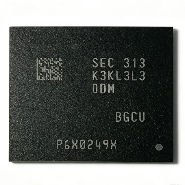
K3KL3L30DM-BGCU - LPDDR5X 64Gb 8533Mbps DRAM | Samsung
K3KL3L30DM-BGCU

K3KL3L30DM-BGCU - LPDDR5X 64Gb 8533Mbps DRAM | Samsung

The Samsung Semiconductor K3KL3L30DM-BGCU is a 64 Gb LPDDR5X low-power DRAM memory IC operating at 8533 Mbps data rate, organized x64, in a 496-ball FBGA package. It operates from multiple supply rails of 1.8 V, 1.05 V, 0.9 V and 0.5 V and is rated for -25 C to +85 C operation. LPDDR (Low Power Double Data Rate) SDRAM is a type of synchronous dynamic random-access memory optimized for mobile and power-sensitive systems. Within the memory hierarchy, LPDDR5X sits at the top of the JEDEC low-power DRAM family (LPDDR4 -> LPDDR5 -> LPDDR5X), functioning as the main-system memory IC that feeds CPUs, GPUs and NPUs in smartphones, tablets, automotive computing platforms and AI edge devices. Key features of the K3KL3L30DM-BGCU include its 8533 Mbps pin speed, which places it in the highest LPDDR5X speed bin, and its 64 Gb density per device, enabling multi-gigabyte system memory with only a few ICs. The x64 organization and 496-ball FBGA footprint allow dense PCB routing on mobile-style boards. Technically, LPDDR5X extends LPDDR5 with higher signaling rates and improved power efficiency. Samsung states its LPDDR5X family delivers up to 8.5 Gbps data processing speeds with approximately 20% better power efficiency than LPDDR5, making it suited to AI inference, high-resolution imaging pipelines and 5G data throughput. Typical applications include flagship smartphone main memory, automotive infotainment and ADAS compute modules, AI edge accelerators, and premium tablet and laptop DRAM subsystems paired with Qualcomm or MediaTek application processors. A key design consideration is power-integrity: LPDDR5X at 8533 Mbps demands tight rail regulation on the 0.5 V VDDQ domain, careful fly-by trace length matching and per-rail decoupling per the memory controller vendor layout guide. This page consolidates distributor stock signals, family cross-references and practical sourcing notes beyond the bare datasheet listing. Pricing is RFQ-based as of 2026-09-04 because this EOL-status part trades through broker channels rather than fixed catalog tiers.

USD $45.94 在庫あり