製品 (39,000+)

NT5CC256M16DP-DIH - 4Gb DDR3L SDRAM 256Mx16 1.35V | Nanya
NT5CC256M16DP-DIH

NT5CC256M16DP-DIH - 4Gb DDR3L SDRAM 256Mx16 1.35V | Nanya

The Nanya NT5CC256M16DP-DIH is a 4Gb DDR3L SDRAM organized as 256Mx16, operating at 1.35V with a 96-ball VFBGA package. It is designed for commercial, industrial, and automotive applications, offering high-speed data transfer with a data rate of 1600 Mbps (DDR3-1600). The device supports auto self-refresh, auto precharge, asynchronous reset, data mask, write leveling, dynamic on-chip termination, and ZQ calibration functions, ensuring robust performance in demanding environments. DDR3L SDRAM is a type of dynamic random-access memory that operates at a lower voltage (1.35V) compared to standard DDR3 (1.5V), reducing power consumption while maintaining high bandwidth. It is part of the DDR3 memory family, which uses double data rate architecture to transfer data on both edges of the clock signal. DDR3L is widely used in computing, networking, and embedded systems where power efficiency is critical. Key features include a 4Gb density, 16-bit I/O width, 1.35V core voltage, and support for industrial temperature range (0°C to +95°C). The device offers programmable CAS latency, burst lengths of 8 and 4, and on-die termination for improved signal integrity. The 96-ball VFBGA package provides a compact footprint suitable for space-constrained designs. The NT5CC256M16DP-DIH utilizes advanced CMOS process technology, achieving high-speed operation with low power dissipation. It incorporates a temperature-compensated self-refresh mechanism to maintain data integrity across temperature variations. The device also features a programmable output driver impedance and supports DLL (Delay-Locked Loop) for precise timing control. Typical applications include DDR3L memory modules for laptops, servers, networking equipment, industrial PCs, and automotive infotainment systems. Its low voltage and high density make it ideal for power-sensitive applications requiring large memory capacity. When designing with this device, ensure proper decoupling capacitors near the power pins and follow the layout guidelines in the datasheet to minimize signal integrity issues. The ZQ calibration pin requires a 240-ohm resistor to ground for correct impedance calibration.

見積もり お問い合わせ
NT5CC256M16DP-FLNA - 4Gb DDR3L SDRAM | Nanya Technology
NT5CC256M16DP-FLNA

NT5CC256M16DP-FLNA - 4Gb DDR3L SDRAM | Nanya Technology

The Nanya Technology NT5CC256M16DP-FLNA is a 4Gb DDR3L SDRAM organized as 256M x 16, operating at 1.35V with a data rate of 1600 Mbps (PC3L-12800). It is housed in a 96-ball BGA package (13x9 mm) and supports commercial, industrial, and automotive temperature ranges. This device is designed for high-bandwidth memory applications requiring low power consumption and reliable performance. DDR3L SDRAM is a type of dynamic random-access memory that operates at a lower voltage (1.35V) compared to standard DDR3 (1.5V), reducing power consumption by up to 20% while maintaining similar performance. It is part of the DDR3 memory family, which uses double data rate architecture to transfer data on both edges of the clock signal, achieving high data rates. DDR3L is commonly used in mobile devices, embedded systems, and industrial applications where power efficiency is critical. Key features include a 16-bit data bus, 8 internal banks, programmable CAS latency (CL 11, 12, 13), burst lengths of 8 and 4 (with burst chop), on-die termination (ODT) for signal integrity, and ZQ calibration for improved timing. The device supports auto self-refresh, auto precharge, and write leveling, ensuring robust operation in various system conditions. It also includes a data mask function and asynchronous reset for enhanced control. The NT5CC256M16DP-FLNA utilizes advanced CMOS technology, achieving low power consumption and high reliability. The 96-ball BGA package provides excellent thermal and electrical performance, with a thermal resistance of [DATA_NEEDED: theta_JA] and operating temperature range of -40°C to +95°C (industrial) and -40°C to +105°C (automotive). The device is RoHS compliant and lead-free. Typical applications include networking equipment (routers, switches), industrial automation, automotive infotainment and ADAS, and embedded computing systems. Its low voltage and high density make it ideal for memory-intensive tasks in space-constrained designs. When designing with this device, ensure proper decoupling capacitors near the power pins and follow the layout guidelines in the datasheet to minimize signal integrity issues. The ZQ pin requires a 240-ohm resistor to ground for calibration.

見積もり お問い合わせ
NT5CC256M16ER-EK - 4Gb DDR3L SDRAM 256Mx16 | Nanya
NT5CC256M16ER-EK

NT5CC256M16ER-EK - 4Gb DDR3L SDRAM 256Mx16 | Nanya

The Nanya NT5CC256M16ER-EK is a 4Gb DDR3L SDRAM organized as 256M x 16, operating at 1.35V with a data rate of 933MHz (DDR3L-1866). It comes in a 96-ball TFBGA package and is designed for commercial and industrial temperature ranges (0°C to +95°C). This memory IC supports auto self-refresh, auto precharge, asynchronous reset, data mask, write leveling, dynamic on-chip termination, and ZQ calibration functions, making it suitable for high-performance computing and embedded systems. DDR3L (Double Data Rate 3 Low Voltage) SDRAM is a type of synchronous dynamic random-access memory that operates at a lower voltage (1.35V) compared to standard DDR3 (1.5V), reducing power consumption while maintaining high bandwidth. It is part of the DDR3 family, which uses double data rate signaling to transfer data on both edges of the clock, and is widely used in laptops, servers, and industrial applications where energy efficiency is critical. Key features include a 4Gb density, 16-bit I/O width, 933MHz clock speed, and support for 1.35V operation. The device also features programmable CAS latency, burst lengths of 8 and 4 (with burst chop), and on-die termination (ODT) for improved signal integrity. The TFBGA-96 package offers a compact footprint suitable for space-constrained designs. Technically, the NT5CC256M16ER-EK uses an 8n-prefetch architecture, achieving high data rates with low power. It includes a mode register for configuration, and supports DLL (Delay-Locked Loop) for precise timing. The device is RoHS compliant and lead-free, meeting environmental standards. Typical applications include DDR3L memory modules for laptops, embedded systems, networking equipment, and industrial PCs. Its low voltage and high density make it ideal for power-sensitive applications. When designing with this component, ensure proper decoupling capacitors near the power pins and follow the layout guidelines in the datasheet to maintain signal integrity at high speeds.

見積もり お問い合わせ
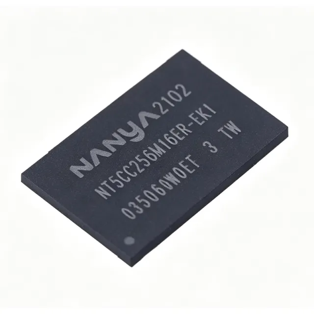
NT5CC256M16ER-EKI - 4Gb DDR3L SDRAM 256Mx16 | Nanya
NT5CC256M16ER-EKI

NT5CC256M16ER-EKI - 4Gb DDR3L SDRAM 256Mx16 | Nanya

The Nanya Technology NT5CC256M16ER-EKI is a 4Gb DDR3L SDRAM organized as 256M x 16, operating at 1.35V (also compatible with 1.5V) in a 96-ball TFBGA package. It is designed for commercial and industrial applications with a temperature range of -40°C to +95°C. This memory component supports data rates up to 933MHz (DDR3L-1866) and includes features such as auto self-refresh, auto precharge, asynchronous reset, write leveling, dynamic on-chip termination, and ZQ calibration. DDR3L SDRAM is a type of double data rate synchronous dynamic random-access memory that operates at a lower voltage (1.35V) compared to standard DDR3 (1.5V), reducing power consumption while maintaining high bandwidth. It is part of the memory hierarchy in computing systems, serving as the main system memory for processors, and is widely used in embedded systems, networking equipment, and industrial PCs. Key features include a 4Gb density, 16-bit data bus, 1.35V core voltage, and support for industrial temperature range. The device uses an 8n-prefetch architecture and supports burst lengths of 8 and 4 (with burst chop). It also features on-die termination (ODT) for improved signal integrity and a programmable CAS latency. The TFBGA-96 package provides a compact footprint suitable for space-constrained designs. Technically, the NT5CC256M16ER-EKI is fabricated using Nanya's advanced DRAM process technology, offering high reliability and low power consumption. The device includes a mode register set (MRS) for configuration, and supports DLL (delay-locked loop) for precise timing. It is compliant with JEDEC DDR3L standards, ensuring interoperability with a wide range of controllers. Typical applications include industrial computing, networking routers and switches, embedded systems, and automotive infotainment. Its industrial temperature rating makes it suitable for harsh environments. The low voltage operation is ideal for battery-powered and energy-efficient designs. When designing with this component, ensure proper decoupling capacitors near the power pins and follow the PCB layout guidelines in the datasheet to minimize signal integrity issues. Also, verify the memory controller supports 1.35V operation for optimal performance.

USD $16.70 お問い合わせ
NT5CC256M16ER-EKT - 4Gb DDR3L SDRAM 256Mx16 | Nanya
NT5CC256M16ER-EKT

NT5CC256M16ER-EKT - 4Gb DDR3L SDRAM 256Mx16 | Nanya

The Nanya NT5CC256M16ER-EKT is a 4Gb (256Mx16) DDR3L SDRAM component operating at a nominal 1.35V, with backward compatibility to 1.5V DDR3 systems. It is housed in a 96-ball TFBGA package and supports DDR3L-1866 (1866 Mbps) with 13-13-13 timing (CL13). This device is designed for commercial and industrial temperature ranges (0°C to +95°C) and includes features such as auto self-refresh, auto precharge, asynchronous reset, data mask, write leveling, dynamic on-chip termination, and ZQ calibration. DDR3L (Double Data Rate 3 Low Voltage) SDRAM is a type of synchronous dynamic random-access memory that operates at a lower voltage (1.35V) compared to standard DDR3 (1.5V), reducing power consumption by up to 20% while maintaining similar performance. It is part of the DDR3 memory family, which uses double data rate signaling to transfer data on both edges of the clock, and is widely used in computing, networking, and embedded systems. Key features include a 4Gb density organized as 256Mx16, a 96-ball TFBGA package, and support for DDR3L-1866 speed grade. The device operates from a 1.35V supply (with 1.5V compatibility) and features programmable CAS latency, burst lengths of 8 and 4 (with burst chop), and on-die termination (ODT) for improved signal integrity. The industrial temperature range option (EKI suffix) is available for harsh environments. Technically, the NT5CC256M16ER-EKT uses an 8n-prefetch architecture with a 16-bit I/O interface, achieving data rates up to 1866 Mbps. It includes a mode register set (MRS) for configuration, DLL for timing alignment, and ZQ calibration for output driver and ODT impedance tuning. The device supports various power-saving modes including power-down and self-refresh, making it suitable for battery-powered applications. Typical applications include DDR3L memory modules for laptops and embedded systems, networking equipment such as routers and switches, industrial automation controllers, and automotive infotainment systems. Its low voltage and high density make it ideal for space-constrained designs requiring high memory bandwidth. When designing with this device, ensure proper decoupling capacitors near the VDD and VDDQ pins, and follow the PCB layout guidelines for DDR3 routing to maintain signal integrity. The ZQ pin requires a 240-ohm resistor to ground for calibration.

見積もり お問い合わせ
NT5CC256M16ER-FLNA - 4Gb DDR3L SDRAM 256Mx16 | Nanya
NT5CC256M16ER-FLNA

NT5CC256M16ER-FLNA - 4Gb DDR3L SDRAM 256Mx16 | Nanya

The Nanya NT5CC256M16ER-FLNA is a 4Gb DDR3L SDRAM organized as 256M x 16 bits, operating at 1.35V with a 96-ball TFBGA package. It is designed for commercial and industrial temperature ranges, supporting data rates up to 1866 Mbps. This memory device features auto self-refresh, auto precharge, asynchronous reset, data mask, write leveling, dynamic on-chip termination, and ZQ calibration, making it suitable for a wide range of computing and embedded applications. DDR3L (Double Data Rate 3 Low Voltage) is a type of synchronous dynamic random-access memory (SDRAM) that operates at a lower voltage (1.35V) compared to standard DDR3 (1.5V), reducing power consumption by about 20% while maintaining similar performance. It is part of the DDR3 family, which uses double data rate signaling to transfer data on both edges of the clock, and is widely used in laptops, servers, and industrial systems where energy efficiency is critical. Key features include a 4Gb density, 16-bit data bus, 1.35V core power supply, and support for 1.5V I/O for compatibility. The device offers programmable CAS latency, burst lengths of 8 and 4 (with burst chop), and on-die termination (ODT) for improved signal integrity. It also includes a temperature sensor for thermal management and supports auto refresh and self refresh modes to maintain data integrity. Architecturally, the NT5CC256M16ER-FLNA uses an 8-bank design with a 16n prefetch architecture, enabling high-speed data transfer. The TFBGA package provides excellent thermal and electrical performance, with a ball pitch of 0.8mm and dimensions of 13mm x 8mm. The device is RoHS compliant and lead-free, meeting environmental standards. Typical applications include DDR3L memory modules for laptops, embedded systems, networking equipment, and industrial PCs. Its low voltage and high density make it ideal for power-sensitive designs, while the industrial temperature grade (-40°C to +95°C) ensures reliable operation in harsh environments. When designing with this device, ensure proper decoupling capacitors near the power pins and follow the layout guidelines in the datasheet to minimize signal integrity issues. The ZQ calibration pin requires a 240-ohm resistor to ground for proper operation.

見積もり お問い合わせ
NT6AN512M32AV-1G - 16Gb LPDDR4 512Mx32 1.1V | Nanya
NT6AN512M32AV-1G

NT6AN512M32AV-1G - 16Gb LPDDR4 512Mx32 1.1V | Nanya

The Nanya NT6AN512M32AV-1G is a high-performance mobile LPDDR4 SDRAM organized as 512M x 32 bits, providing 16Gb (2GB) of memory density. It operates at a supply voltage of 1.1V and supports data rates up to 4267 Mbps (LPDDR4-4267), making it suitable for bandwidth-intensive applications in smartphones, tablets, AI edge devices, and embedded systems. The device is housed in a 200-ball BGA package, enabling compact PCB designs. LPDDR4 (Low Power Double Data Rate 4) is a type of synchronous DRAM designed for mobile and low-power applications. It achieves high bandwidth while operating at lower voltages (1.1V) compared to standard DDR4 (1.2V), reducing power consumption in battery-powered devices. LPDDR4 is part of the JEDEC LPDDR memory standard family, which includes LPDDR2, LPDDR3, LPDDR4, and LPDDR5, each offering increased speed and efficiency. As a mobile DRAM, it is optimized for low-power operation and high-density packaging, making it essential for modern portable electronics. Key features include a 16Gb density with a 512M x 32 organization, 1.1V core power supply, and support for data rates up to 4267 Mbps. The device includes a built-in temperature sensor for Temperature Compensated Self Refresh (TCSR), which adjusts refresh rates based on temperature to save power. It also supports ZQ calibration for DS/ODT impedance accuracy via an external ZQ pad (240Ω ± 1%) and Data Bus Inversion (DBI) to reduce power consumption and improve signal integrity. The 200-ball BGA package is designed for space-constrained applications. Technically, the NT6AN512M32AV-1G utilizes advanced DRAM process technology to achieve high density and low power. The device supports dual-channel operation in multi-die packages (DDP/QDP) for higher capacity. It includes features like DQ calibration for signal synchronization, training for signal synchronization, and a temperature sensor for TCSR. These features ensure reliable operation across a wide temperature range, making it suitable for industrial and automotive applications. Typical applications include mobile devices (smartphones, tablets), AI computers, video conferencing systems, and industrial control systems. The high bandwidth and low power consumption make it ideal for AI edge inference, where large data sets are processed locally. In video conferencing, the high data rate supports multiple high-resolution video streams simultaneously. When designing with this device, ensure proper power decoupling with 0.1uF and 1uF capacitors near the power pins. Follow the JEDEC LPDDR4 layout guidelines for signal integrity, especially for high-speed data lines. The ZQ pin requires a 240Ω ± 1% resistor to ground for impedance calibration.

見積もり お問い合わせ
NT6AN8T0SA - 2Gb LPDDR2 SDRAM | Nanya Technology
NT6AN8T0SA

NT6AN8T0SA - 2Gb LPDDR2 SDRAM | Nanya Technology

The NT6AN8T0SA is a high-performance, low-power mobile LPDDR2 SDRAM manufactured by Nanya Technology Corporation. It is designed for space-constrained, battery-powered applications requiring high memory density and low power consumption. The device operates at a low supply voltage of 1.2V, making it ideal for portable electronics where power efficiency is critical. The NT6AN8T0SA is available in a compact FBGA package, enabling high-density board layouts in smartphones, tablets, and other mobile devices. LPDDR2 (Low Power Double Data Rate 2) SDRAM is a type of synchronous dynamic random-access memory optimized for low power consumption in mobile and embedded systems. It is part of the DDR memory family, which includes DDR2, DDR3, and DDR4, but is specifically designed to operate at lower voltages (1.2V) and provide power-saving features such as deep power-down and partial-array self-refresh. LPDDR2 is widely used in smartphones, tablets, and portable consumer electronics, where battery life is a primary concern. Key features of the NT6AN8T0SA include a 2Gb density, a 32-bit I/O width, and support for data rates up to 1066 Mbps (533 MHz). The device operates from a 1.2V power supply, with an I/O voltage of 1.2V, and supports a temperature range of -30°C to +85°C. It includes features such as programmable latency, burst length of 4 or 8, and on-die termination (ODT) for improved signal integrity. The device is RoHS compliant and lead-free, meeting environmental standards. Technically, the NT6AN8T0SA utilizes a 4-bank architecture with a 2Gb density, organized as 64M x 32. It supports auto-refresh and self-refresh modes, with a refresh period of 64ms at 85°C. The device features a programmable output driver impedance and supports DLL (Delay-Locked Loop) for precise timing. The low-voltage operation and advanced power management features make it suitable for always-on applications, such as IoT devices and wearables. Typical applications include smartphones, tablets, portable media players, and embedded systems requiring high memory bandwidth with minimal power consumption. The NT6AN8T0SA is also used in automotive infotainment systems and industrial handheld devices where reliability and low power are essential. When designing with the NT6AN8T0SA, ensure proper decoupling capacitors are placed near the power pins to minimize noise. The device requires a stable 1.2V supply and careful PCB layout to maintain signal integrity at high data rates. Refer to the manufacturer's datasheet for detailed timing and layout guidelines.

見積もり お問い合わせ
NT6AN8T6WBJ1B1 - 8Gb DDR4 SDRAM | Nanya Technology
NT6AN8T6WBJ1B1

NT6AN8T6WBJ1B1 - 8Gb DDR4 SDRAM | Nanya Technology

The NT6AN8T6WBJ1B1 is a high-performance 8Gb DDR4 SDRAM manufactured by Nanya Technology, organized as 512M x 16 bits. It operates at a data rate of 3200 MT/s (PC4-25600) with a supply voltage of 1.2V, compliant with JEDEC DDR4 standards. The device is housed in a 96-ball FBGA package, enabling high-density memory solutions for computing, networking, and industrial applications. DDR4 SDRAM (Double Data Rate 4 Synchronous Dynamic Random-Access Memory) is a type of volatile memory that transfers data on both edges of the clock signal, doubling the data rate compared to DDR3. It operates at lower voltages (1.2V) and higher speeds, offering improved power efficiency and bandwidth. DDR4 is the industry standard for main memory in servers, desktops, and laptops, and is also used in embedded systems requiring high-speed data processing. Key features include a burst length of 8 (BL8) with burst chop (BC4), on-die termination (ODT) for signal integrity, and programmable CAS latency (CL) of 22 cycles. The device supports auto-refresh and self-refresh modes for power saving, and includes a temperature sensor for thermal management. The 1.2V supply reduces power consumption by up to 20% compared to DDR3L, making it suitable for energy-efficient designs. Architecturally, the NT6AN8T6WBJ1B1 uses an 8n-prefetch architecture with a 16-bit I/O interface, achieving a peak bandwidth of 25.6 GB/s per module. It incorporates bank groups (4 groups of 4 banks) to improve concurrency and reduce latency. The device supports write leveling and read leveling for robust signal integrity in high-speed systems, and includes a built-in self-test (BIST) feature for manufacturing and system diagnostics. Typical applications include DDR4 memory modules (UDIMM, SODIMM, RDIMM), embedded computing, networking equipment (routers, switches), and industrial automation. Its high density and speed make it ideal for servers and data centers requiring large memory capacity and fast data throughput. When designing with this device, ensure proper decoupling capacitors (0.1uF and 10uF) are placed near the VDD and VDDQ pins, and follow the JEDEC DDR4 layout guidelines for trace impedance (40-50 ohms) and length matching. The device requires a stable 1.2V supply and a separate 1.2V VDDQ for the I/O, with a reference voltage (VREF) of 0.6V.

見積もり お問い合わせ
NTB0102GT,115 - 2-Bit Auto-Direction Level Translator | NXP
NTB0102GT,115

NTB0102GT,115 - 2-Bit Auto-Direction Level Translator | NXP

The NXP Semiconductors NTB0102GT,115 is a 2-bit dual-supply translating transceiver with auto direction sensing and 3-state outputs, delivering bidirectional voltage level translation at data rates up to 100 Mbps in an 8-pin XSON SOT833-1 package measuring just 1.95 mm x 1 mm. A dual-supply translating transceiver is a logic IC that bridges two voltage domains on a PCB - for example a 1.8 V microcontroller port and a 3.3 V or 5 V peripheral. It sits within the logic IC family hierarchy under voltage level translators and bus transceivers, forming part of the broader power management and interface logic ecosystem. Unlike direction-controlled translators, auto-direction sensing devices detect data flow automatically, removing the need for a DIR control pin. Key features include dual supply rails - VCC(A) from 1.2 V to 3.6 V and VCC(B) from 1.65 V to 5.5 V - a fast 4.8 ns propagation delay, automatic direction sensing on both I/O ports, and a shared output enable (OE) input that 3-states both ports for bus isolation. The 100 Mbps data rate comfortably covers I2C, SPI, UART, and general-purpose GPIO translation. Architecturally, the NTB0102 uses NXP's auto-direction sensing scheme with open-drain style I/O structures and integrated 10 kohm pull-up resistors on the A-side, so the dominant driver determines direction on a per-bit basis without host intervention. This eliminates bus contention and firmware overhead in mixed-voltage systems. Typical applications include translating SPI or I2C buses between 1.8 V MCUs and 3.3 V sensors, level-shifting UART links in battery-powered products, and interfacing 5 V legacy peripherals to low-voltage processors. Design consideration: because auto-direction translators rely on weak pull-ups, use them with push-pull, lightly loaded buses; heavily capacitive or resistive loads reduce the effective data rate. This page adds value beyond the datasheet with verified drop-in alternatives, distributor pricing context, FAQ answers to real engineer queries, and practical design notes.

見積もり お問い合わせ
NTB0102GT,115 - 2-Bit Auto-Direction Level Translator | NXP
NTB0102GT115

NTB0102GT,115 - 2-Bit Auto-Direction Level Translator | NXP

The NXP Semiconductors NTB0102GT,115 is a 2-bit dual-supply translating transceiver with auto direction sensing, delivering bidirectional voltage level translation at data rates up to 100 Mbps in a space-saving 8-pin XSON SOT833-1 package measuring just 1.95 x 1 mm. A dual-supply translating transceiver is a type of voltage level shifter within the broader logic IC family. Its role in the system hierarchy is to bridge digital domains operating at different supply voltages - for example a 1.8 V microcontroller port communicating with a 3.3 V peripheral. Unlike direction-controlled transceivers, auto direction sensing parts eliminate a DIR pin, using the data itself to determine signal flow, which simplifies firmware and board design. Key features include a VCC(A) supply range of 1.2 V to 3.6 V and a VCC(B) range of 1.65 V to 3.6 V, supporting virtually any low-voltage logic pairing including 1.2 V to 3.3 V translation. The output enable (OE) input 3-states all I/Os when low, and partial power-down operation (Ioff) protects both supplies during power sequencing. The 100 Mbps throughput comfortably covers I2C-fast-class, SPI, UART, and general-purpose GPIO translation. Architecturally, the NTB0102 uses a transmission-gate based topology with pull-up keepers on each I/O. Because the keepers are weak, bus holding is suitable for lightly capacitive lines; strongly driven push-pull sources on either side determine direction dynamically. This makes the part ideal for point-to-point links rather than heavily loaded multidrop buses. Typical applications include microcontroller-to-peripheral GPIO and SPI translation, open-drain I2C and SMBus bus translation with appropriate pull-ups, and level shifting between low-voltage FPGA or SoC banks and 3.3 V system logic. Design consideration: the weak bus keepers mean the NTB0102 is best suited to push-pull driven signals; for heavily loaded multidrop buses, consider the push-pull driver NTS0102 family variant instead. This page synthesizes distributor pricing context, drop-in alternatives, and practical design notes not found in the manufacturer datasheet, with all data verified as of 2026-10-19.

見積もり お問い合わせ
NTE74LS08 - Quad 2-Input AND Gate, TTL LS, DIP-14 | NTE Electronics
NTE74LS08

NTE74LS08 - Quad 2-Input AND Gate, TTL LS, DIP-14 | NTE Electronics

The NTE Electronics NTE74LS08 is a Low-Power Schottky TTL logic integrated circuit containing four independent 2-input positive AND gates in a 14-lead plastic DIP (PDIP-14) through-hole package. It operates from a 4.75V to 5.25V supply, delivers up to 8.8 mA output drive, and features a typical propagation delay of 20 ns at 5V with a 15 pF load. A quad AND gate is a combinational logic device whose output goes HIGH only when both of its inputs are HIGH; the 'quad 2-input' designation means the package integrates four such gates sharing only power and ground. AND gates form the foundation of digital logic hierarchy, sitting alongside NAND, OR, and NOT gates within the broader transistor-transistor logic (TTL) family and the wider class of small-scale integration (SSI) logic ICs. Key features of the NTE74LS08 include Low-Power Schottky (LS) process technology, which uses Schottky-clamped transistors to combine the speed of standard TTL with significantly reduced power consumption, a commercial temperature grade suitable for bench and service environments, and through-hole mounting ideal for prototyping, breadboarding, and repair work. Each gate output sinks and sources current compatible with other TTL and many CMOS loads. Architecturally, the LS family's Schottky diode clamping prevents transistor saturation, cutting storage time and enabling propagation delays around 20 ns while keeping per-gate power draw low relative to standard 7400-series TTL. The NTE74LS08 is NTE Electronics' direct replacement numbering for the industry-standard 74LS08 function, widely used in maintenance, repair, and overhaul (MRO) contexts. Typical applications include legacy industrial control logic, address decoding in vintage computing and test equipment, signal interlock and enable-gating circuits in instrumentation, and educational digital logic laboratory work. The through-hole DIP-14 package makes it especially well suited to socketed replacements on older PCBs. A key design consideration: as a bipolar TTL device, unused inputs should not be left floating - tie them to VCC through a 1 kOhm to 10 kOhm resistor or to a driven output to avoid noise-induced oscillation. This page synthesizes distributor pricing, drop-in alternatives, a full DIP-14 pinout, and practical design notes not found in the manufacturer datasheet. Note that NTE Electronics permanently closed operations in late 2024, so stock is available only through remaining distributor and excess inventory channels; the industry-standard equivalents listed here are the recommended path for new designs.

見積もり お問い合わせ
NTE922 Low-Input-Current Voltage Comparator | NTE Electronics
NTE922

NTE922 Low-Input-Current Voltage Comparator | NTE Electronics

The NTE Electronics NTE922 is a low-input-current voltage comparator supporting supply operation from single 5 V logic supplies through standard plus-or-minus 15 V analog supplies. It is offered in an eight-pin metal-can package and provides open-collector transistor outputs. According to the NTE922 datasheet, its input currents are nearly one thousand times lower than those of the NTE910 and NTE910D comparators, making it useful when sensing or switching nodes has a high source impedance. A voltage comparator is an integrated circuit that compares two input voltages and produces a digital logic state indicating which input is higher. Within the semiconductor hierarchy, the NTE922 is a comparator, then a logic IC and an analog interface device. Unlike an operational amplifier configured as a comparator, this device is intended specifically for threshold decision-making rather than linear signal amplification. Its open-collector outputs allow wired logic and pull-up resistors to be used in many interface circuits. The principal verified feature is extremely low input current, nearly one thousand times lower than the NTE910 or NTE910D. This characteristic helps minimize loading on high-impedance sources, reference dividers, sensor outputs, and charge-balanced detection networks. The wider supply range lets the same comparator family support conventional plus-or-minus 15 V analog systems and 5 V digital logic systems, although each exact electrical limit must be confirmed from the manufacturer datasheet before a production design is released. NTE922, NTE922M, and NTE922SM are three package variants of the same comparator family. The supplied evidence identifies NTE922 as the eight-pin metal-can version, while NTE922M and NTE922SM are associated with different mounting packages. The wider supply range lets the same comparator family support conventional plus-or-minus 15 V analog systems and 5 V digital logic systems, although each exact electrical limit must be confirmed from the manufacturer datasheet before a production design is released. Typical uses include high-impedance threshold detection, low-current sensing, pulse and timing systems, interface logic, legacy industrial equipment, and repair or modernization of circuits originally designed around NTE comparators. Because the output is open collector, designers must include suitable pull-up resistors and account for the output's sink-current and switching limitations when setting fanout or load capacitance. A critical design check is the input common-mode range. A wide supply-voltage rating does not guarantee that both inputs remain within their linear operating region near the supply rails. Prototype the divider and test both threshold polarities while observing output polarity. Also route the high-impedance input node with short traces, guard it where practical, and keep leakage from board contamination and flux from creating false transitions. This page combines verified family-level data, packaging distinctions, replacement constraints, and application guidance. Exact electrical values not present in the supplied evidence remain flagged rather than guessed, and any replacement must be checked for package pins, output topology, supply range, input bias current, common-mode range, and timing before it is treated as a drop-in part.

見積もり お問い合わせ

NTS0302JK - 2-Bit Dual Supply Level Transceiver | NXP
NTS0302JK

NTS0302JK - 2-Bit Dual Supply Level Transceiver | NXP

The NXP Semiconductors NTS0302JK is a 2-bit, dual-supply translating transceiver with open-drain outputs and auto direction sensing, enabling bidirectional voltage level translation between two independent power domains. It features two 1-bit input-output ports (A and B), one output enable input (OE), and two supply pins, and is supplied in an NXP small-footprint package (JK suffix) for space-constrained boards. A dual-supply translating transceiver is a class of voltage level shifter IC within the logic and interface IC hierarchy. Unlike direction-controlled transceivers, auto direction sensing devices monitor the bus and reverse transmission direction without a DIR control pin, which removes firmware overhead and eliminates bus contention caused by incorrect direction settings. Open-drain ports additionally allow pull-up resistors to set each side's logic high level independently, supporting mixed-voltage I2C-style, open-drain, or slowly switching signaling. Key features include fully bidirectional translation with no direction pin, open-drain A and B ports for flexible pull-up voltage selection, an OE input to place ports in the high-impedance state, and independent VCCA and VCCB supplies so either side can be powered down without latch-up risk. This architecture suits 1.2 V to 5 V rail combinations typical in mixed-voltage embedded systems. The auto direction sensing engine detects which side is driving and propagates the state to the opposite side with short propagation delay, making the part suitable for two-wire and multi-drop open-drain buses. Because the ports are open drain, rise time is set by the external pull-up resistor and bus capacitance, giving designers direct control of edge rates for EMI management. Typical applications include I2C and SMBus level shifting between 3.3 V microcontrollers and 5 V peripherals, GPIO translation in mixed-supply industrial and automotive body-electronics modules, and open-drain status or interrupt lines bridging power domains. Design consideration: size the pull-up resistors so the RC rise time meets bus timing; excessively strong pull-ups increase sink current through the NTS0302 open-drain stages. Tie OE to the appropriate level when translation must always be active. This page synthesizes distributor pricing context, alternative strategy, and practical design notes not found in the manufacturer datasheet.

見積もり お問い合わせ
NTS0304EUKZ - 4-Bit Dual-Supply Level Translator | NXP
NTS0304EUKZ

NTS0304EUKZ - 4-Bit Dual-Supply Level Translator | NXP

The NXP Semiconductors NTS0304EUKZ is a 4-bit dual-supply translating transceiver with open-drain outputs and auto-direction sensing, housed in a 12-ball WLCSP (1.42 x 1.97 mm) package. VCC(A) can be supplied at any voltage between 0.95 V and 3.6 V, enabling bidirectional voltage level translation between mixed-voltage systems without a direction-control pin. A dual-supply level translator is a type of voltage-level conversion IC, part of the broader logic family of buffers, drivers and transceivers within the signal-integration hierarchy of semiconductor components. Its role is to safely connect digital devices operating at different supply rails, such as a 1.8 V microcontroller and a 3.3 V peripheral, preventing overvoltage damage and logic-level misreads that would occur with direct connection. Key features include four independent bidirectional channels with automatic direction sensing, which eliminates the need for a DIR pin and simplifies bus designs; open-drain outputs supporting open-drain buses such as I2C-style topologies; and a single output enable (OE) input that places all I/O in a high-impedance state when deasserted. Architecturally, the device features eight 1-bit input-output ports (A and B ports), one OE input, and two supply pins (VCC(A) and VCC(B)). Because outputs are open-drain, external pull-up resistors set the logic-high level on each side, allowing rail levels to be chosen almost independently of the supply voltages. According to the NXP NTS0304E product data sheet Rev. 1.3 (9 October 2023), this makes the family well suited to mixed-voltage bidirectional signaling. Typical applications include I2C and SMBus level shifting between controllers and peripherals, bidirectional GPIO translation between MCUs of different voltage classes, and mixed-voltage board-to-board communication. The WLCSP package suits space-constrained portable and wearable designs. Design consideration: because the outputs are open drain, always provide appropriate pull-up resistors sized for the bus capacitance and desired rise time; the auto-direction sensing requires the bus to default high. This page synthesizes distributor pricing, drop-in alternatives, design notes, and application guidance not found in the manufacturer datasheet.

見積もり お問い合わせ
NTS0308EPWJ - 8-Bit Auto-Direction Level Translator | NXP
NTS0308EPWJ

NTS0308EPWJ - 8-Bit Auto-Direction Level Translator | NXP

The NXP Semiconductors NTS0308EPWJ is an 8-bit, dual-supply translating transceiver with open-drain outputs and auto direction sensing, providing bidirectional voltage level translation at data rates up to 20 Mbps in a 20-pin TSSOP (PW) package. VCC(A) supports 0.95 V to 3.6 V and VCC(B) supports 1.0 V to 3.6 V, enabling translation between any two logic levels in these ranges. A dual-supply level translator is a power management and interface device that bridges digital circuits operating at different voltage domains, for example a 1.8 V microcontroller communicating with a 3.3 V sensor. Within the signal-integrity hierarchy, the NTS0308E belongs to the level translator family, a subcategory of interface ICs (logic translators), which sit above simple buffers in complexity because they must manage two independent supply rails and direction control. Key differentiating features include auto direction sensing, which eliminates the need for a direction-control pin because each I/O automatically detects whether it should act as an input or output; open-drain outputs, which allow the device to work with I2C-style pull-up buses and mixed-voltage open-drain signalling; and a single output-enable (OE) input that tri-states all eight channels for power savings. The wide 0.95 V VCC(A) floor supports emerging sub-1.2 V logic cores. Architecturally, each of the eight A/B ports uses a one-bit input-output cell that senses the applied voltage level and drivers, sourcing current only during rising edges to limit dynamic supply current - a technique that also permits use with pull-up resistors on partially powered buses. The open-drain structure means external pull-up resistors set the high level at each side, giving designers full flexibility over bus levels. Typical applications include I2C and SMBus bus level shifting between 1.8 V, 2.5 V, and 3.3 V domains, interfacing low-voltage microcontrollers to 3.3 V peripherals, mixed-voltage open-drain bus translation in industrial and automotive body-electronics modules, and general-purpose 8-bit bidirectional level shifting in consumer and IoT hardware. Design-wise, note that because outputs are open drain, pull-up resistors are mandatory and effective data rate falls as pull-up resistance and bus capacitance rise; the 20 Mbps figure assumes light RC loading. Keep VCC(A) and VCC(B) decoupled with 0.1 uF ceramics close to the pins. This page adds value beyond the manufacturer datasheet by consolidating distributor pricing, drop-in alternative analysis, application-specific design notes, and AEO-optimized Q&A in one place.

見積もり お問い合わせ
NTSX2102 - 2-Bit Open-Drain Level Translator | NXP | I2C
NTSX2102

NTSX2102 - 2-Bit Open-Drain Level Translator | NXP | I2C

The NXP Semiconductors NTSX2102 is a 2-bit dual-supply translating transceiver with open-drain outputs and automatic direction sensing, delivering bidirectional voltage level translation at up to 50 Mbit/s in a 8-pin XQFN package measuring just 1.4 x 1.2 mm (NTSX2102GU8H). A dual-supply translating transceiver is a class of level-shifter IC within the broader hierarchy of logic ICs and voltage translators. It bridges two independently powered domains - for example a 1.8V microcontroller and a 3.3V peripheral - by translating logic thresholds between a VCC(A) side and a VCC(B) side. Open-drain architectures are specifically suited to shared buses such as I2C and 1-wire, where lines are pulled high by external resistors and any device can drive them low, requiring no explicit direction control signal. The NTSX2102's headline features are automatic direction sensing (no DIR pin required), an output enable input (OE) that tri-states both ports for bus isolation or power-down, and an open-drain output structure purpose-built for I2C, SMBus-style and 1-wire point-to-point links. Two 2-bit input/output port pairs (A1/A2 and B1/B2) provide the translation channels. According to the NXP product data sheet, the device is targeted at point-to-point applications interfacing devices or systems operating at different supply voltages, using open-drain drivers. The auto-direction-sensing topology detects which side is driving and propagates the transition to the opposite side, eliminating firmware direction management. The 50 Mbit/s capability comfortably covers Standard, Fast and Fast-mode Plus I2C speeds as well as faster proprietary 2-wire links. Typical applications include I2C bus level translation between 1.8V/3.3V domains, 1-wire EEPROM and authentication IC links, low-voltage sensor interfaces in portable and battery-powered systems, and general-purpose open-drain signaling where footprints of a few square millimeters matter. Design consideration: open-drain translation requires external pull-up resistors on both sides; choose pull-up values that balance rise time (bus capacitance) against static current, and ensure the A-side supply is not below the device minimum - an NXP community thread notes operation starts from 1.65 V on the A-side, so 1.2 V domains need a different part. This page synthesizes distributor listings, drop-in alternative analysis, and practical design notes not found in the manufacturer datasheet.

見積もり お問い合わせ
NUC029SEE - Cortex-M0 72MHz 128KB Flash MCU | Nuvoton
NUC029SEE

NUC029SEE - Cortex-M0 72MHz 128KB Flash MCU | Nuvoton

The Nuvoton NUC029SEE is a 32-bit microcontroller with an embedded Arm Cortex-M0 core, operating at up to 72 MHz with 128 KB of embedded Flash memory, housed in a 64-pin LQFP (7x7 mm) package. It operates from a 2.5V to 5.5V supply across a -40C to +105C industrial temperature range. A microcontroller unit (MCU) is a single-chip computer that integrates a processor core, non-volatile program memory, SRAM, and peripherals on one die. MCUs sit at the device level of the embedded-system hierarchy (semiconductor -> integrated circuit -> microcontroller -> embedded control system), executing dedicated control tasks in appliances, industrial machines, and connected devices. Key features of the NUC029SEE include the crystal-less USB 2.0 full-speed device controller, which eliminates an external crystal and reduces BOM cost and board area; a 22.1184 MHz high-precision internal oscillator with +/-1% accuracy at 25C and 5V (full-range +/-3%); and robust electromagnetic immunity with ESD tolerance up to HBM 7 kV and EFT 4.4 kV. Peripherals include RTC, CRC, and I2C among a rich peripheral set typical of the NuMicro NUC029 series. Architecturally, the Arm Cortex-M0 core delivers 32-bit computing with a compact instruction set and low gate count, suited to cost-sensitive industrial control. The wide 2.5V-5.5V operating window allows direct connection to 3.3V or 5V logic domains without level shifting, a significant advantage in mixed-voltage legacy industrial designs. The NuMicro NUC029 series is specifically engineered for industrial control applications requiring robust immunity and strong anti-interference capability. Typical applications include industrial control and automation, USB-connected devices and bridges, motor control front ends, and home appliances requiring wide-voltage, wide-temperature operation. The crystal-less USB device feature makes the part especially attractive for compact USB peripherals where board space and cost dominate. When designing with the NUC029SEE, use the internal oscillator within its stated accuracy envelope, and add an external crystal only if USB or UART timing demands tighter tolerance than +/-1% (at 25C, 5V). Confirm Flash and SRAM sizing against code growth before selecting the 128 KB SEE variant over smaller family members. This page synthesizes distributor pricing, verified drop-in alternatives, and practical design notes not found in the manufacturer datasheet alone.

見積もり お問い合わせ
NUC120RD3AN - 32-bit Cortex-M0 MCU 64KB Flash 64-LQFP | Nuvoton
NUC120RD3AN

NUC120RD3AN - 32-bit Cortex-M0 MCU 64KB Flash 64-LQFP | Nuvoton

The Nuvoton NUC120RD3AN is a 32-bit ARM Cortex-M0 microcontroller from the NuMicro NUC120 series running at up to 50 MHz, with 64KB (64K x 8) of embedded Flash program memory, 16KB SRAM, and 45 general-purpose I/O lines, housed in a 64-pin LQFP (7x7 mm) package operating from a 3.3V/5V supply. A microcontroller (MCU) is a single integrated circuit that combines a processor core, memory, and peripherals into one chip, forming the lowest tier of the embedded processing hierarchy: MCU -> embedded processor -> SoC. The ARM Cortex-M0 core used here is the most energy-efficient 32-bit ARM processor, delivering performance comparable to many 16-bit MCUs at a cost equivalent to traditional 8-bit devices, which is why it is widely used as an 8-bit replacement in cost-sensitive designs. Key features of the NUC120RD3AN include USB 2.0 device connectivity, a rich peripheral set (I2C, SPI, UART/USART, IrDA, I2S, PWM, EBI/EMI), and support functions such as brown-out detect/reset, DMA, low-voltage detect, power-on reset, and a watchdog timer. The internal oscillator eliminates the need for an external crystal in many designs, and four-level priority NVIC interrupt handling supports 32 interrupt inputs. Architecturally, the device couples the Cortex-M0 core with the NuMicro NUC100-series peripheral fabric; Keil MDK device support confirms full CMSIS-compliant toolchain compatibility for the NUC120RD3AN. Typical applications include USB-connected industrial controllers, consumer appliance control panels, motor control with PWM, and communication bridges using its multiple serial interfaces. Design consideration: confirm supply window (3.3V/5V tolerant operation) and verify Flash/RAM sizing against application footprint, as 64KB/16KB is adequate for most control tasks but not for large protocol stacks. This page synthesizes distributor pricing, drop-in alternatives, and practical design notes not found in the manufacturer datasheet.

見積もり お問い合わせ
NVT2002DP,118 - 2-Bit Bidirectional Level Translator 1.0-5V | NXP
NVT2002DP,118

NVT2002DP,118 - 2-Bit Bidirectional Level Translator 1.0-5V | NXP

The NXP Semiconductors NVT2002DP,118 is a 2-bit bidirectional voltage-level translator that operates from 1.0 V to 3.6 V on the A side and from 1.8 V to 5.5 V on the B side, allowing bidirectional voltage translation between 1.0 V and 5 V without a direction pin, in an 8-pin TSSOP (DP) package. A voltage level translator (also called a level shifter or voltage translator) is a mixed-signal interface IC that safely connects digital devices operating at different supply voltages, such as a 1.8 V microcontroller and a 5 V sensor. Level translators sit within the broader hierarchy of logic ICs and interface ICs in the signal chain, forming a bridge between voltage domains in power management and system I/O design. Without translation, direct connection risks over-voltage damage or failure to meet logic thresholds. Key features of the NVT2002 include direction-pin-free operation, which simplifies control firmware and eliminates bus contention logic; support for both open-drain and push-pull applications; identical electrical characteristics across both channels with minimal output-to-output deviation; and low effective line capacitance for signal speeds below 33 MHz in open-drain mode. The architecture uses reference voltages Vref(A) and Vref(B) with an enable (EN) input that, when LOW, places all I/O in the high-impedance state, significantly reducing supply current. Technically, the NVT2002 employs a pass-gate architecture: a one-shot edge accelerator briefly lowers the output impedance on rising edges to overcome the RC time constant of the pull-up resistors, while a bias network between Vref(B) and Vref(A) holds the bus near the A-side threshold. This hybrid approach combines the bidirectionality of open-drain schemes with the low capacitance and speed of transistor-switch designs, avoiding the propagation-delay penalty of dual-supply CMOS translators. Typical applications include I2C, SMBus, and PMBus level shifting between 3.3 V controllers and 5 V peripherals, GPIO and UART interface translation in mixed-voltage embedded systems, and low-speed bus bridging in industrial and automotive body-electronics modules where microcontrollers such as NXP and ST MCUs interface to 5 V sensors and actuators. One key design consideration: because the translator is open-drain at its core, push-pull operation requires proper pull-up resistor sizing - lower values improve edge rates but increase static current through the internal bias network, so engineers must trade speed against power consumption. This page synthesizes distributor pricing, drop-in alternatives, practical design notes, and an application-by-application selection guide not found in the manufacturer datasheet, verified as of 2026-10-19.

見積もり お問い合わせ
NVT2002DP118 - 2-Bit Bidirectional Level Translator | NXP
NVT2002DP118

NVT2002DP118 - 2-Bit Bidirectional Level Translator | NXP

The NXP Semiconductors NVT2002DP,118 (NVT2002DP118) is a 2-bit bidirectional voltage level translator operating from 1.0 V to 3.6 V on the A-side reference (VREF(A)) and 1.8 V to 5.5 V on the B-side reference (VREF(B)), enabling bidirectional translation between 1.0 V and 5 V logic domains in an 8-pin TSSOP (SOT505) package. A voltage level translator, also called a logic level shifter, is a signal-integrity interface IC that converts digital signals between circuits operating at different supply voltages. Within the signal-conversion hierarchy, the level translator sits under interface ICs and logic ICs, bridging mismatched voltage domains such as a 1.8 V microcontroller GPIO bank talking to a 5 V legacy peripheral, without loss of signal integrity. Key features include true bidirectional operation without a direction pin, support for both open-drain and push-pull applications, a 1.0 V low-side capability that supports the latest low-voltage cores, and an enable (EN) pin that places all outputs in the high-impedance state when the device is disabled, reducing system power. All channels share identical electrical characteristics, so channel-to-channel skew is minimal - important for multi-bit buses. Technically, the NVT2002 uses a one-shot architecture built around a reference-driven pass gate: VREF(A) sets the low-voltage domain, VREF(B) sets the high-voltage domain, and the internal one-shot accelerates rising edges so propagation delay stays in the nanosecond range for push-pull use. Because the I/O structure behaves like an open-drain output with pull-up to the local reference, it also transparently supports I2C-style open-drain buses at voltages from 1.0 V to 5 V. Typical applications include interfacing 1.8 V MCUs to 3.3 V or 5 V sensors, I2C/SMBus level shifting between mixed-voltage domains, translating UART and SPI control lines in industrial systems, and bridging legacy 5 V logic to modern low-voltage processors. Design consideration: pull-up resistor sizing on open-drain buses directly sets rise time and bus speed; follow the datasheet recommendations to balance current draw against edge rate at your target data rate. This page synthesizes distributor pricing, drop-in family alternatives, and practical design notes not found in the manufacturer datasheet.

見積もり お問い合わせ
NVT4557HKX - SIM Card Level Translator, ESD | NXP
NVT4557HKX

NVT4557HKX - SIM Card Level Translator, ESD | NXP

The NXP Semiconductors NVT4557HKX is a SIM card interface level translator with integrated EMI filtering and ESD protection, housed in a 10-pin XQFN package. It translates data, RSTn, and CLKn signals between a low-voltage host interface of 1.08 V to 1.98 V and a SIM card side operating from 1.62 V to 3.6 V, with 15 ns propagation delay and 10 MHz signaling support. A level translator (also called a voltage level shifter or voltage translator) is an interface IC that allows digital circuits operating at different supply voltages to communicate reliably. In the power-management and interface hierarchy, the NVT4557 sits between a host microcontroller and a smart card, bridging the voltage gap created by modern low-voltage SoCs that no longer generate the higher SIM card supply rails internally. The device complies with ISO-7816 SIM/smart card interface requirements. Key features include three dedicated 1.62 V to 3.6 V level translators for data, reset (RSTn), and clock (CLKn) lines, integrated EMI filtering that suppresses radiated and conducted emissions on the SIM lines, and built-in ESD protection that removes the need for external transient-voltage-suppression diodes on the card interface. Because the device provides supply translation without an internal LDO, it simplifies the bill of materials in designs where the card supply is already generated elsewhere. Technically, the part supports an operating temperature range of -40 C to +85 C, making it suitable for both consumer and industrial embedded designs. The XQFN10 package keeps the footprint minimal for space-constrained mobile, IoT, and M2M hardware. Fast 15 ns transitions support the 10 MHz SIM clocking modes required by modern LTE and 5G modules. Typical applications include SIM card interfaces in cellular modems, LTE/5G gateways, point-of-sale terminals, telematics units, and IoT devices using eSIM or removable SIM form factors. When designing with the NVT4557HKX, keep the host supply within the 1.08 V to 1.98 V window and ensure the card-side supply stays within 1.62 V to 3.6 V; place the device close to the SIM connector to maximize the benefit of the integrated EMI filter. This page synthesizes distributor pricing, lifecycle status, design notes, and selection guidance not found in the manufacturer datasheet alone.

見積もり お問い合わせ
NVT4558HKX - SIM Card Level Translator 10-XQFN | NXP
NVT4558HKX

NVT4558HKX - SIM Card Level Translator 10-XQFN | NXP

The NXP Semiconductors NVT4558HKX is a SIM card interface level translator with integrated EMI filter and ESD protection, housed in a 10-pin XQFN (1.4 mm x 1.8 mm) package. It interfaces host processors operating from 1.2 V to 1.8 V with SIM cards operating from 1.8 V to 3.6 V, supporting bidirectional data transfer at up to 10 MHz. A level translator (also called a voltage level shifter or logic translator) is a type of interface IC within the broader logic IC family that converts digital signals between circuits operating at different supply voltages. In modern mobile and IoT systems, low-voltage baseband processors (1.2 V to 1.8 V) must communicate with SIM/UICC cards that may run at 1.8 V or 3 V class voltages (up to 3.6 V). Without translation, direct connection risks overvoltage damage or unreliable logic thresholds. The NVT4558HK family solves this in a single, protection-integrated device. Key differentiating features include integrated ESD protection on all card-side pins rated to 8 kV contact discharge per IEC 61000-4-2, integrated EMI filtering that suppresses higher harmonics of the digital I/O signals (important for passing regulatory EMC testing in cellular devices), and a bidirectional translation architecture with a 10 MHz data rate that comfortably covers the ISO 7816-compatible clock rates used by 3GPP SIM interfaces. Architecturally, the device combines automatic direction-sensing translation channels for the SIM data line with supply-domain isolation between the host side (1.2 V to 1.8 V) and card side (1.8 V to 3.6 V). The integration of the EMI filter and ESD structures into the same die eliminates discrete TVS diodes and filter components, reducing BOM count and PCB area in space-constrained designs such as smartphones, cellular modules, and M2M terminals. Typical applications include SIM card interfaces in 4G/5G cellular modems, eUICC/SIM sockets in IoT trackers, telematics control units, and payment terminals, all of which require reliable low-voltage to card-voltage translation with robust ESD immunity at the externally accessible card contacts. Design consideration: keep the card-side traces short and place the device close to the SIM connector so the integrated EMI filter and ESD structures provide maximum benefit; verify that the host-side supply stays within the 1.2 V to 1.8 V range for correct logic thresholds. This page synthesizes distributor pricing, drop-in alternatives, and practical design notes not found in the manufacturer datasheet.

見積もり お問い合わせ
NVT4858HKZ - SD/SDIO Level Translator 104Mbps | NXP
NVT4858HKZ

NVT4858HKZ - SD/SDIO Level Translator 104Mbps | NXP

The NXP Semiconductors NVT4858HKZ is an SD 3.0-compliant bidirectional dual-supply voltage level translator with auto-direction control, 6 translation channels, 104 Mbps data rate support, integrated EMI filtering and ESD protection, housed in a 16-pin XQFN (1.8 x 2.6 mm) package. The HKZ suffix denotes the version without an integrated LDO regulator. A voltage level translator is a logic IC that safely interfaces digital signals between circuit domains operating at different supply voltages. In the memory-card hierarchy, the level translator sits between a host processor or MCU and the SD/SDIO/microSD/SIM card slot, converting logic thresholds so that a 1.08 V to 1.98 V host controller can communicate with a card running at 1.62 V to 3.6 V. Without translation, over-voltage on a low-voltage host IO would violate absolute maximum ratings and damage the SoC. Key features include full SD 3.0 SDR104 compliance at 104 Mbps, automatic direction control that removes the need for a direction pin, six bidirectional channels covering the CLK, CMD and DAT[0:3] card signals, and built-in EMI filtering that reduces radiated emissions on the card interface. On-chip ESD protection hardens the card pins against electrostatic discharge events encountered during card insertion and removal. Architecturally, the NVT4858 uses a dual-rail pass-gate translation core with auto-direction sensing on each channel, so the translator detects whether the host or the card is driving and mirrors the level accordingly. This is essential for open-drain phases of the SD protocol where the bus direction reverses dynamically within a transaction. Typical applications are microSD and SD card slots in smartphones, tablets, automotive infotainment head units, embedded Linux boards and IoT gateways, plus SIM card interfaces in cellular modems. Design consideration: the HKZ variant has no internal LDO, so the card-side supply must be generated externally with a clean, current-limited rail to preserve signal integrity at SDR104 speeds. This page synthesizes distributor pricing, drop-in alternatives, and practical design notes not found in the manufacturer datasheet.

見積もり お問い合わせ