Produk (39,000+)

ADS1286U - 12-Bit 20kHz Micro Power ADC | Texas Instruments
ADS1286U

ADS1286U - 12-Bit 20kHz Micro Power ADC | Texas Instruments

The Texas Instruments ADS1286U is a 12-bit, 20 kHz micro-power sampling analog-to-digital converter (ADC) with a differential input, integrated sample-and-hold amplifier, and a high-speed SPI/SSI-compatible serial interface, housed in an 8-pin SOIC package. The device draws only 250 uA of supply current, operates from a single 4.5 V to 5.25 V supply, and guarantees no missing codes across the full temperature range. An analog-to-digital converter is a mixed-signal integrated circuit that converts a continuous-time, continuous-amplitude analog signal into a discrete digital code. The ADS1286 belongs to the successive-approximation-register (SAR) ADC product family within the broader signal-chain taxonomy that includes sigma-delta, pipeline, and flash converters. SAR ADCs are favored for low-power, single-shot, and multiplexed data-acquisition tasks because they offer deterministic latency, compact silicon area, and inherently low power consumption compared with higher-resolution delta-sigma parts. Key specifications of the ADS1286U include 12-bit resolution, a 20 kHz maximum sampling rate, an integral non-linearity of +/-1 LSB (max), and a SINAD of 72 dB. The differential input stage accepts a +/-Vref full-scale range (typically 0 V to 5 V single- or 5 V differentially) and is preceded by a sample-and-hold that eliminates the need for an external front-end amplifier in most applications. The serial interface is clock-synchronized and supports two- or three-wire operation with an external serial clock rate up to 4 MHz, easing isolation between the converter and the host microcontroller. Architecturally, the ADS1286 uses a charge-redistribution SAR core with a thin-film laser-trimmed input scaling network; this topology yields the very low 250 uA quiescent current while preserving 12-bit DC accuracy. The internal reference loop is designed for use with an external 2.5 V or 5 V reference, and the device does not include an on-chip reference. The wide-input-range CMOS input structure simplifies sensor-bridge and thermocouple front ends. Typical end-use applications for the ADS1286U include battery-powered instrumentation, remote data loggers, isolated industrial sensors, portable medical devices, and handheld meters. Its tiny 8-pin SOIC footprint and 250 uA supply current make it especially attractive for loop-powered 4-20 mA transmitters and other energy-harvested nodes where every microamp matters. A practical design consideration is the addition of an anti-aliasing RC filter ahead of the analog inputs: a 1 kohm/10 nF single-pole filter is sufficient for a 20 kHz Nyquist boundary. Decouple VDD with a 0.1 uF ceramic placed within 5 mm of the supply pin. This page synthesizes distributor pricing, verified drop-in alternatives, and practical layout notes not found on generic catalog summaries.

RFC Hubungi kami
ADS1286U/2K5G4 - 12-Bit 20kHz Micropower SAR ADC | TI
ADS1286U/2K5G4

ADS1286U/2K5G4 - 12-Bit 20kHz Micropower SAR ADC | TI

The Texas Instruments ADS1286U/2K5G4 is a 12-bit, 20 kHz successive-approximation analog-to-digital converter (SAR ADC) with a differential input and integrated sample-and-hold amplifier, packaged in an 8-pin SOIC (0.154", 3.90 mm width) and consuming only 250 µA of supply current. It supports a single-ended or differential analog input over a 0 V to 5.3 V range and a 5 V nominal supply, providing SPI/SSI-compatible two- or three-wire serial communication for microcontroller, FPGA, or DSP hosts. This micropower combination of low supply current and a 20 kSPS sample rate makes it well suited to battery-powered and isolated data-acquisition front ends. A successive-approximation ADC (often abbreviated SAR ADC) is a type of data-conversion IC that walks an internal capacitive DAC from MSB to LSB each conversion cycle, producing a low-latency, deterministic sample output with no pipeline delay. SAR ADCs are widely used when a system needs a clean single-shot sample with simple control, low standby current, and modest resolution - they sit between slower sigma-delta ADCs (which trade latency for higher resolution) and flash ADCs (which trade power for speed). Within a system, the SAR ADC is positioned just after analog signal conditioning and ahead of a digital controller that consumes the conversion result. Key features include guaranteed no missing codes at 12 bits, 20 kHz maximum sampling rate, 250 µA typical supply current, an SPI/SSI-compatible serial interface, a single 5 V supply, and an industrial -40 °C to +85 °C operating temperature range. The 8-SOIC footprint and two-wire serial interface simplify board layout and reduce MCU pin overhead in space-constrained designs. The architecture combines an input sample-and-hold with a charge-redistribution SAR core and a precision internal reference path, giving deterministic latency of one conversion cycle and the absence of pipeline or integration delay. Because the digital interface is a simple shift-register readout, the part is straightforward to drive from virtually any microcontroller with an SPI peripheral. Typical applications include remote sensor data acquisition, isolated analog front ends, battery-powered instrumentation, industrial process-control transducers, and portable medical accessory boards. The DIP and SOIC footprints also support hand-soldered prototype or through-hole-style retrofit boards. When designing the analog front end, take care to bypass VDD with a 0.1 µF ceramic close to the pin and to keep the analog input traces short and guarded, since the 12-bit, 20 kSPS converter will expose any added noise or reference drift directly in the conversion result. This page consolidates distributor pricing, pin-compatible drop-in alternatives, and practical design guidance not found in the standalone manufacturer datasheet.

RFC Hubungi kami
ADS1286UC/2K5 - 12-Bit 20kHz Micro-Power SAR ADC | Texas Instruments
ADS1286UC/2K5

ADS1286UC/2K5 - 12-Bit 20kHz Micro-Power SAR ADC | Texas Instruments

The Texas Instruments ADS1286UC/2K5 is a 12-bit, 20 kHz successive-approximation analog-to-digital converter (SAR ADC) with a differential input and integrated sample-and-hold amplifier, supplied in an 8-pin SOIC package and tape-and-reel packaging. According to the TI ADS1286 datasheet, the device consumes only 250 µA of supply current, supports an SPI/SSI-compatible serial interface (two- or three-wire), and guarantees no missing codes across the full operating range. The differential input and 0-5 V analog input range make it well suited to bridge-sensor, transducer, and battery-monitoring front-ends where ground-loop rejection matters. An SAR ADC (Successive Approximation Register Analog-to-Digital Converter) is a type of data converter that uses a binary search algorithm and an internal DAC to resolve an analog input one bit per clock cycle. SAR ADCs sit within the broader hierarchy: ADC → data converter → mixed-signal IC → semiconductor. Compared to delta-sigma ADCs, SAR converters offer deterministic latency, no pipeline delay, and lower power consumption at sample rates up to a few MSPS, which is why they remain the workhorse for multiplexed data-acquisition systems and motor-control current sensing. Key differentiating specifications include 12-bit resolution with no missing codes, 20 kHz maximum sample rate, 250 µA quiescent supply current, and a wide single-supply operating range (typically 4.5 V to 5.25 V). The integrated differential input eliminates the need for external instrumentation amplifiers in many sensor-conditioning paths, and the synchronous serial interface allows direct connection to microcontrollers and DSPs without glue logic. Architecture-wise, the ADS1286 combines a capacitive-charge-distribution DAC, a high-gain comparator, and an SAR control logic block. A single conversion cycle takes 16 internal clock periods, with the sample-and-hold acquiring on the falling edge of CS and conversion starting on the rising edge. The device requires an external reference voltage and an external serial clock, keeping the analog front-end compact and predictable. Typical applications include portable instrumentation, weigh scales, remote sensors, process-control loops, and battery-powered data loggers. Industrial-grade temperature range (-40 °C to +85 °C) and the small SOIC-8 footprint suit it to space-constrained embedded designs. A primary design consideration is the input common-mode range, which must stay within the supply rails; for true bipolar signals, consider a true bipolar-input ADC such as the ADS1287 family. The /CS pin doubles as the conversion-start trigger, so firmware timing must respect the 16-clock conversion window to avoid corrupted results. This page synthesizes distributor pricing, drop-in alternatives, and practical design notes not found in the manufacturer datasheet.

RFC Hubungi kami
ADS1286UK/2K5 - 12-Bit 20kHz Micro Power SAR ADC | Texas Instruments
ADS1286UK/2K5

ADS1286UK/2K5 - 12-Bit 20kHz Micro Power SAR ADC | Texas Instruments

The Texas Instruments ADS1286UK/2K5 is a 12-bit, 20 kHz successive-approximation-register (SAR) analog-to-digital converter with a differential input and on-chip sample-and-hold, supplied in an 8-pin SOIC (D) package. Operating from a single 4.5 V to 5.25 V analog supply, the device draws only 250 µA typical supply current, integrating low-power conversion with a synchronous serial (SPI/SSI-compatible) data interface. An SAR ADC is a precision converter that uses a binary-weighted capacitor array and a comparator to perform a bit-by-bit decision against the analog input during each conversion cycle. SAR converters sit in the data-converter IC family, which also includes delta-sigma, pipeline, and dual-slope architectures; SAR parts are valued for deterministic latency, single-shot accuracy, and low power, which makes them well suited to multiplexed sensor readout, industrial monitoring, and battery-powered instrumentation. Within TI's converter portfolio, the ADS1286 occupies the micropower SAR niche where sample rate and channel count are modest but quiescent current is critical. Key specifications include 12-bit no-missing-codes resolution, a 20 kHz maximum sample rate, differential analog input, an external reference (VREF), an integrated sample-and-hold amplifier, and SPI/SSI-compatible two- or three-wire serial output. The part is specified across the -40 °C to +85 °C industrial temperature range and supports an 8-SOIC footprint that is pin-compatible with several legacy and current TI 8-pin ADC and DAC devices, enabling board-level reuse. According to the Texas Instruments ADS1286 datasheet, the device includes an active-low CS (chip-select, falling-edge frame) and an SCLK-driven bit clock, with DOUT changing on the falling SCLK edge to simplify glueless MCU interfacing. Typical applications include portable and battery-powered sensor digitizers, transducer and bridge-sensor signal conditioning, industrial process-control analog front ends, isolated-data-acquisition modules, and replacement of legacy 12-bit ADC subsystems. The 250 µA supply current makes the part especially attractive for loop-powered 4-20 mA transmitters and remote data loggers where standby current dominates battery life. When designing, place the 0.1 µF VDD bypass capacitor as close as possible to pin 8 and keep the analog/digital ground return paths short; a clean external reference is mandatory for full 12-bit accuracy, and the SOIC-8 footprint allows standard reflow profiles.

RFC Hubungi kami
ADS1292RIPBS - 2-Ch 24-Bit AFE Biopotential ECG | Texas Instruments
ADS1292RIPBS

ADS1292RIPBS - 2-Ch 24-Bit AFE Biopotential ECG | Texas Instruments

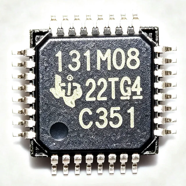
The Texas Instruments ADS1292RIPBS is a 2-channel, 24-bit, simultaneous-sampling analog front-end (AFE) for biopotential measurements, integrating a low-noise programmable gain amplifier (PGA), a delta-sigma analog-to-digital converter (ADC), an internal reference, and an onboard oscillator in a 32-pin TQFP (PBS) 5x5 mm package. The 'R' suffix indicates the integrated respiration impedance measurement function alongside the two ECG/EMG channels, and the part is rated for 740 uW typical power consumption at 1 kSPS. An analog front-end (AFE) is a mixed-signal subsystem that conditions low-amplitude physiological signals (typically 1 uV to 5 mV) and digitizes them so a host processor can run diagnostic algorithms. In the hierarchy of medical electronics, AFEs sit between the electrode/sensor interface and the digital signal controller (DSC) or microcontroller, replacing the discrete instrumentation amplifier plus separate 16-/24-bit ADC approach with a single qualified, low-power IC. The ADS1292 family is optimized for electrocardiogram (ECG), electromyography (EMG), and electroencephalography (EEG) front-end designs where low input-referred noise and high common-mode rejection are mandatory for diagnostic accuracy. Key features include 2 high-resolution 24-bit delta-sigma ADCs with simultaneous sampling up to 8 kSPS per channel, integrated PGA gains from 1 to 12, an integrated respiration modulation/demodulation circuit, a 2.7 V to 5.25 V analog supply range, a 1.8 V to 3.6 V digital I/O supply, and a flexible SPI-compatible serial interface. The device provides right-leg drive (RLD) signal generation hardware, lead-off detection comparators, and an internal oscillator that eliminates the external crystal requirement in cost-sensitive wearable designs. Architecturally, the ADS1292 uses a chopper-stabilized input front-end combined with a 4th-order delta-sigma modulator and a multi-bit digital decimation filter to achieve input-referred noise in the microvolt range while drawing sub-milliwatt quiescent current. The integrated respiration channel uses a high-frequency AC excitation source and synchronous demodulator to extract breathing impedance without an external analog multiplier IC. Typical applications include wearable fitness and heart-rate monitors, single-lead and multi-lead ECG patches, patient-side telemetry modules, sports and EMG rehabilitation devices, and bioimpedance-based sleep monitors. The wide supply range supports both single-cell Li-ion battery designs (3.7 V nominal) and USB-powered diagnostic instruments (5 V bus). When designing with this device, ensure the analog and digital ground planes are joined at a single point under the IC exposed pad, place the 1 uF, 0.1 uF, and 10 uF decoupling capacitors as close as possible to AVDD and DVDD pins, and route the right-leg drive (RLD) amplifier output through a feedback network sized for the patient-electrode return path to maximize common-mode rejection at 50/60 Hz mains frequencies.

RFC Hubungi kami
ADS1298CZXGT - 8-Ch 24-Bit ECG AFE, 64-NFBGA | Texas Instruments
ADS1298CZXGT

ADS1298CZXGT - 8-Ch 24-Bit ECG AFE, 64-NFBGA | Texas Instruments

The Texas Instruments ADS1298CZXGT is a low-power, 8-channel, 24-bit analog front-end (AFE) for biopotential measurements, integrating eight simultaneously-sampling delta-sigma analog-to-digital converters (ADCs) with built-in programmable gain amplifiers (PGAs), reference voltage, and an on-board oscillator in a 64-pin NFBGA (ZXG) 8x8 mm package. The device delivers 14.1 mW total power dissipation while providing 24-bit resolution across all eight channels, with a maximum data rate of 32 kSPS per channel and 8 kSPS in high-resolution mode, optimized for clinical electrocardiogram (ECG), electromyography (EMG), and electroencephalography (EEG) acquisition systems. An analog front-end (AFE) for biopotential measurements is a highly integrated signal-chain block that combines low-noise amplification (typically via a PGA), anti-alias filtering, and high-resolution sigma-delta conversion directly at the sensor interface. AFEs sit above general-purpose ADCs in the signal-chain hierarchy - they replace the traditional discrete chain of instrumentation amplifier + filter + ADC with a single IC, reducing board area, noise, and design complexity. The ADS1298 family in particular adds integrated right-leg drive (RLD) amplifiers, lead-off detection, Wilson central terminal (WCT) generation, and pace detection, making it a complete biopotential AFE rather than a generic ADC. Key features include eight simultaneously-sampling 24-bit sigma-delta ADCs, integrated PGA gains from 1 to 12 V/V, a low input-referred noise of approximately 4 uVPP at 150 Hz BW (gain = 6), selectable data rates from 500 SPS to 32 kSPS, built-in right-leg drive amplifier, lead-off detection, and a flexible SPI-compatible serial interface. The on-chip 2.5 V reference and internal oscillator reduce external component count, while the integrated pace-detection circuitry supports three-channel pace pulse detection for Holter and patient-monitoring equipment. The device uses a switched-capacitor delta-sigma modulator architecture per channel, followed by a digital decimation filter, achieving high common-mode rejection (>100 dB at 50/60 Hz) and excellent dynamic range for small biopotential signals (typically 1-5 mV ECG amplitude). The digital filter chain supports simultaneous 50 Hz / 60 Hz line rejection, simplifying international product compliance. The 64-ball NFBGA package has a thermal resistance of approximately 32 C/W and supports the commercial 0 C to +70 C operating range specified for the CZXGT suffix. Typical applications include 12-lead clinical ECG monitors, portable patient telemetry, Holter recorders, brain-computer interfaces (EEG), sports and fitness ECG wearables, and instrumentation-grade EMG systems. The eight-channel density also suits multi-modal acquisition boards combining ECG, respiration (impedance pneumography), and pulse oximetry front-end channels on a single chip. When designing with this AFE, pay close attention to PCB layout: keep the analog input traces short and guarded, place the 2.2 uF decoupling capacitors immediately adjacent to each AVDD pin, and avoid routing digital SPI traces near the analog inputs to preserve the >100 dB CMRR. Use the integrated right-leg-drive amplifier to reduce common-mode pickup rather than relying on external instrumentation amplifiers. This page synthesizes XAIPART distributor pricing, drop-in same-package alternatives from TI's ADS129x family, and practical layout notes for medical biopotential designs that the manufacturer datasheet alone does not provide.

RFC Hubungi kami
ADS1298IPAG - 8-Ch 24-Bit ECG AFE, 14.1mW | Texas Instruments
ADS1298IPAG

ADS1298IPAG - 8-Ch 24-Bit ECG AFE, 14.1mW | Texas Instruments

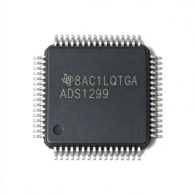
The Texas Instruments ADS1298IPAG is a low-power, 8-channel, 24-bit simultaneous-sampling delta-sigma analog-to-digital converter with integrated biopotential (ECG/EEG) front-end, packaged in a 64-pin TQFP (PAG, 10x10 mm). It integrates eight low-noise programmable gain amplifiers (PGAs), eight 24-bit ADCs, an internal reference, and an onboard oscillator, and dissipates 14.1 mW total (approximately 0.75 mW per channel) at full data rate. An analog front-end is the signal-conditioning and conversion stage placed between analog physiological sensors and a digital host processor. In the broader component taxonomy, the ADS1298IPAG is an AFE -> data converter (ADC) -> mixed-signal IC -> semiconductor. Delta-sigma ADCs use oversampling and noise shaping to achieve very high resolution (24-bit) at the cost of absolute input bandwidth, making them the standard choice for low-frequency, high-precision biopotential measurements where microvolt-level signals must be resolved in the presence of large DC offsets and 50/60 Hz line interference. Key features of the ADS1298IPAG include 4 uVPP input-referred noise (at 150 Hz bandwidth with gain = 6), 200 pA input bias current, built-in right-leg drive (RLD) amplifier, on-chip Wilson central terminal (WCT) generator for 12-lead ECG derivation, internal lead-off detection, and a flexible SPI-compatible serial interface. Eight channels are sampled simultaneously, eliminating skew between leads in multi-channel ECG/EMG recordings. The device operates from a unipolar analog supply of 2.7 V to 5.5 V (AVDD) and a digital I/O supply of 1.65 V to 3.6 V (DVDD). Its input common-mode range and high CMRR (typical > -100 dB) allow direct connection to skin electrodes without external instrumentation amplifiers. The integrated PGA offers gains from 1 to 12, supporting sensor signals ranging from sub-millivolt EEG to several-millivolt EMG. Typical applications include 12-lead clinical ECG monitors, portable patient telemetry, Holter recorders, EEG/EMG front-ends, evoked-potential biopotential acquisition, sleep-stage monitors, and bioimpedance research accessories. When using this device, ensure the unused channels are tied to AVDD (not GND) to prevent ESD paths from injecting noise; place AVSS and DGND ground returns as a star ground near the IC; and bypass AVDD/AVSS with 10 uF + 0.1 uF ceramic pairs within 5 mm of the pins.

RFC Hubungi kami
ADS1299-6PAG - 6-Ch 24-Bit Low-Noise AFE for EEG/Biopotential | TI
ADS1299-6PAG

ADS1299-6PAG - 6-Ch 24-Bit Low-Noise AFE for EEG/Biopotential | TI

The Texas Instruments ADS1299-6PAG is a 6-channel, 24-bit, low-noise, simultaneous-sampling delta-sigma analog-to-digital converter (ADC) with an integrated programmable gain amplifier (PGA), internal reference, and onboard oscillator, housed in a 64-pin TQFP (PAG) package measuring 10x10 mm. It is part of the ADS1299-x family of 4-, 6-, and 8-channel AFEs designed for high-resolution biopotential measurements and delivers input-referred noise of 1 uVPP at 70 Hz bandwidth, CMRR of -110 dB, and a data rate from 250 SPS to 16 kSPS. The integrated PGA offers programmable gains of 1, 2, 4, 6, 8, 12, and 24, allowing direct connection to low-amplitude electrodes without external instrumentation amplifiers. A biopotential analog front end (AFE) is a specialized mixed-signal IC that combines low-noise amplification, multi-pole analog filtering, and high-resolution digitization in a single chip, replacing the traditional discrete chain of instrumentation amp + anti-alias filter + ADC. In the broader system hierarchy, an AFE sits at the signal-chain boundary between the analog sensor domain (electrodes, transducers) and the digital processing domain (MCU/DSP/FPGA). The ADS1299-6 specifically addresses extracranial electroencephalogram (EEG), electrocardiogram (ECG), electromyography (EMG), and brain-computer interface (BCI) applications where the combination of sub-uV noise floor, high common-mode rejection, and simultaneous multi-channel sampling is mandatory. Key features include 1 uVPP input-referred noise at 70 Hz BW, -110 dB CMRR, programmable gain from 1 to 24 in 7 discrete steps, internal 4.033 V reference, internal oscillator, and daisy-chain capability for high channel-count systems. The device supports SPI-compatible serial communication and consumes approximately 33 mW total, with a flexible right-leg drive (RLD) loop per channel for bias electrode driving. The 64-TQFP package provides ample thermal headroom for portable multi-channel designs. Architecturally, the ADS1299-6 uses a third-order delta-sigma modulator per channel followed by a digital SINC filter chain, achieving simultaneous sampling by sharing a common DRDY signal. The integrated PGA front-end, matched with the modulator's low-noise input stage, allows the device to resolve signals in the sub-uV range critical for EEG micro-features. Internal calibration and self-test routines plus a dedicated bias amplifier streamline biopotential front-end designs. Typical applications include clinical-grade EEG headsets, research-grade BCI platforms, polysomnography, ECG/EMG patient monitors, evoked-potential instrumentation, and bioimpedance research front-ends. The simultaneous-sampling architecture preserves inter-channel phase relationships required for source localization and coherence analysis in neuroscience research. When designing with this part, careful PCB layout of the analog ground plane, dedicated low-noise LDO rails for AVDD/AVSS, and proper patient-electrode bias return are essential to realize the 1 uVPP noise specification. Use the daisy-chain interface when extending beyond 6 channels by stacking additional ADS1299-x devices on the same SPI bus. This page synthesizes distributor stock, drop-in cross-reference options, and practical biopotential design considerations not found in the manufacturer datasheet alone, accelerating your EEG/BCI/biomedical product development.

USD $22.05 Dalam Stok
ADS1299IPAGR - 8-Ch 24-Bit AFE for EEG/Biopotential | Texas Instruments
ADS1299IPAGR

ADS1299IPAGR - 8-Ch 24-Bit AFE for EEG/Biopotential | Texas Instruments

The Texas Instruments ADS1299IPAGR is a low-noise, 8-channel, 24-bit, simultaneous-sampling delta-sigma analog-to-digital converter (ADC) with a built-in programmable gain amplifier (PGA), internal reference, and onboard oscillator, packaged in a 64-pin TQFP (PAG, 10x10 mm). It offers 8 differential input channels, a maximum data rate of 16 kSPS per channel, and an input-referred noise of approximately 0.5 uVpp (gain = 24), making it the highest-performance member of the TI biopotential AFE family. An analog front end (AFE) is an integrated circuit that combines a low-noise analog signal chain (typically PGA, filters, and ADC reference) with the digitizing converter on a single die. The ADS1299 belongs to the broader hierarchy of mixed-signal data converters, then successive-approximation or delta-sigma ADCs, and finally precision measurement ICs that interface directly with low-amplitude physiological sensors. By integrating the biasing, lead-off detection, and right-leg drive drivers required for EEG/ECG/EMG, the AFE reduces the external component count compared to a discrete ADC-plus-op-amp solution. Key features include a PGA with gains from 1 to 24 in 7 steps, internal 4.5 V low-drift reference (30 ppm/C typical), internal oscillator, and selectable SPI-compatible serial interface. Input common-mode rejection exceeds 110 dB at 60 Hz, and the integrated bias amplifier supplies patient or subject bias in active electrode circuits. Power consumption is approximately 42 mW per channel with all channels active, while a flexible power-down mode reduces current to microamp levels for wearable battery-powered applications. Architecturally, the device uses a chopper-stabilized, multi-bit delta-sigma modulator per channel followed by a digital decimation filter. This topology achieves the very low input-referred noise necessary for sub-microvolt biopotential signals while suppressing 1/f and mains interference. The internal reference and oscillator eliminate two critical external components that typically drift across temperature in discrete designs. Typical applications include electroencephalography (EEG) headsets, polysomnography and sleep monitoring, electrocardiography (ECG/Holter) patient monitors, electromyography (EMG) prosthetics, brain-computer interfaces (BCI), and electrophysiology research instrumentation. In EEG systems the part's CMRR and noise floor allow detection of microvolt-scale cortical signals without complex shielding. When designing with the ADS1299, place the device on a four-layer PCB with a continuous analog ground plane, route the analog inputs as guarded differential pairs, and use a clean low-noise LDO such as the TPS7A4701 for AVDD to preserve noise performance. Always refer to the manufacturer datasheet and the ADS1299 evaluation module (ADS1299EEGFE-PDK) reference design for layout guidance.

RFC Hubungi kami
ADS131E08SPAGR - 8-Ch 24-Bit 64-kSPS Delta-Sigma ADC | TI
ADS131E08SPAGR

ADS131E08SPAGR - 8-Ch 24-Bit 64-kSPS Delta-Sigma ADC | TI

The Texas Instruments ADS131E08SPAGR is a multichannel, simultaneous-sampling, 24-bit, delta-sigma analog-to-digital converter (ADC) delivering data rates up to 64 kSPS on eight channels, packaged in a 64-pin TQFP (PAG, 10x10 mm) and specified from -40C to +105C. Power consumption is a low 17.6 mW. An analog front-end (AFE) is a circuit block that conditions and digitizes analog signals before digital processing. Within the signal-chain hierarchy (delta-sigma ADC -> analog front-end -> data acquisition system -> signal chain), the ADS131E08S is a complete AFE that integrates eight delta-sigma converters, programmable gain amplifiers (PGAs), an internal voltage reference, and an internal oscillator in a single IC, drastically reducing the component count of multi-channel data acquisition systems. Key features include 24-bit resolution across eight simultaneous channels, a 64 kSPS maximum sample rate, differential or pseudo-differential inputs, an SPI serial interface, and a fast power-up/start-up time. Simultaneous sampling is essential for power monitoring because phase relationships between voltage and current channels must be preserved for accurate power calculations. Architecturally, each channel uses a delta-sigma modulator with an internal digital decimation filter, providing noise shaping and high resolution at moderate bandwidth. The fast start-up specification enables quick power-on to valid conversion data, which is critical for protection relays that must detect and respond to faults within milliseconds. The integrated PGA allows direct connection of sensors with varying output levels without external amplification. Typical applications include grid protection relays, power quality analyzers, energy metering, and industrial motor monitoring, where eight synchronized channels capture three-phase voltage and current waveforms. The 1.8V digital / 5V analog supply configuration fits standard industrial rails. Design consideration: decouple the analog and digital supplies independently and maintain a single, quiet ground plane; isolate the SPI bus when it crosses to noisy digital domains to preserve the specified noise floor. Price data as of 2026-08-30.

RFC Hubungi kami
ADS131M08 - 8-Ch 24-Bit 32kSPS Delta-Sigma ADC | TI
ADS131M08

ADS131M08 - 8-Ch 24-Bit 32kSPS Delta-Sigma ADC | TI

The Texas Instruments ADS131M08 is an eight-channel, simultaneously-sampling, 24-bit delta-sigma (ΔΣ) analog-to-digital converter (ADC) offering wide dynamic range, low power, and energy-measurement-specific features. Housed in a 32-pin TQFP (PBS, 5x5 mm) package, it suits energy metering, power metrology, and circuit breaker applications. A delta-sigma ADC oversamples the input signal and applies digital filtering to achieve very high resolution, making this converter category the dominant choice for precision measurements such as power metering. Within the signal-chain hierarchy, the ADS131M08 sits between analog front-end conditioning (resistor dividers, current transformers, shunts) and the digital MCU that processes energy computations. Key features include eight simultaneously sampling differential inputs, programmable output data rate up to 32 kSPS, and programmable gain up to 128. Noise performance is 102-dB dynamic range at gain = 1 and 4 kSPS, and 80-dB dynamic range at gain = 64 and 4 kSPS. The device integrates a low-drift internal voltage reference, allowing ADC inputs to interface directly to resistor-divider networks or current-sensing elements without external precision references. The simultaneous-sampling architecture is critical for polyphase energy metering: all eight channels convert at the same instant, preserving phase relationships between voltage and current channels needed for accurate active, reactive, and apparent power calculations. The ADS131M08 is AEC-Q100 qualified (temperature grade 1, -40C to +125C ambient) and Functional Safety-Capable, with documentation available to support functional safety system design, enabling automotive and industrial metering use. Typical applications include three-phase smart energy meters, power quality analyzers, protective relay and circuit breaker monitoring, and solar inverter MPPT sensing. In a bidirectional interleaved buck-converter reference design, TI pairs the ADS131M08 with a C2000 MCU for precise current and voltage control. Design tip: at gain = 64 the input-referred noise rises, so size shunt resistance and gain together to balance dynamic range against full-scale headroom.

RFC Hubungi kami
ADS131M08IPBS - 8-Ch 24-Bit 32kSPS Delta-Sigma ADC | TI
ADS131M08IPBS

ADS131M08IPBS - 8-Ch 24-Bit 32kSPS Delta-Sigma ADC | TI

The Texas Instruments ADS131M08IPBS is an eight-channel, simultaneously-sampling, 24-bit delta-sigma (ΔΣ) analog-to-digital converter (ADC) with a programmable output data rate up to 32 kSPS and programmable gain up to 128, housed in a 32-pin TQFP (5x5 mm) package. A delta-sigma ADC oversamples the analog input and applies digital decimation filtering to reach very high resolution, which makes this converter family the dominant architecture for precision power and metrology sensing. Within the signal-chain hierarchy, the ADS131M08 sits between front-end conditioning (resistor dividers or current transformers, which its inputs can directly interface to) and a host MCU communicating over its serial interface. Key features include eight simultaneously sampling differential inputs, a programmable output data rate up to 32 kSPS, and a programmable gain amplifier with settings up to 128. Noise performance is 102-dB dynamic range at gain = 1 (4 kSPS) and 80-dB dynamic range at gain = 64 (4 kSPS), enabling direct connection to shunt resistors and current transformers without external amplification in many designs. Energy-measurement-specific features reduce external component count in metering front ends. The architecture uses a delta-sigma modulator per channel with digital filter and decimation stages, plus a serial interface with CRC options for robust communication. Because all eight channels sample at the same instant, phase relationships across channels are preserved - critical for three-phase power calculations. An automotive variant, the ADS131M08QPBSRQ1, is AEC-Q100 qualified for temperature grade 1 and functional-safety-capable with supporting documentation. Typical applications include three-phase energy meters, protective relays and circuit breakers, solar inverter and power metrology systems, and motor drive current/voltage sensing. In a bidirectional interleaved buck converter reference design, TI pairs the ADS131M08 with a C2000 MCU for precise power-stage control. Design tip: because all channels sample simultaneously, external network tolerances (divider ratio, shunt value) dominate inter-channel accuracy - budget external precision accordingly rather than relying on ADC matching alone. This page synthesizes distributor pricing, drop-in same-family alternatives, comparison tables, and practical design notes not found in the manufacturer datasheet alone.

USD $3.85 Hubungi kami
ADS131M08IPBSR - 24-Bit 8-Ch 32kSPS Delta-Sigma ADC | TI
ADS131M08IPBSR

ADS131M08IPBSR - 24-Bit 8-Ch 32kSPS Delta-Sigma ADC | TI

The Texas Instruments ADS131M08IPBSR is an 8-channel, simultaneously-sampling, 24-bit delta-sigma (ΔΣ) analog-to-digital converter delivering 32 kSPS per channel through a serial SPI interface, housed in a 32-pin TQFP (PBS) 5x5 mm package on tape and reel. A simultaneous-sampling delta-sigma ADC is a precision data-converter architecture in which every channel is digitized at the same instant by its own ΔΣ modulator, eliminating the skew and phase error inherent to multiplexed ADCs. Within the signal-chain hierarchy (sensor front end -> precision ADC -> digital controller), simultaneous sampling is essential for power metrology, where voltage and current channels must be phase-aligned to compute real power, power factor, and harmonic content accurately. Key features include full 24-bit resolution, per-channel oversampling with programmable data rates up to 32 kSPS, wide dynamic range, and low power operation. TI designed the family with energy-measurement-specific features such as a dedicated CRC on the serial interface for communication integrity, direct interfacing to resistor-divider networks and current transformers or Rogowski-coil front ends, and synchronized clocking across multiple devices for polyphase metering. Architecturally, each of the eight channels integrates its own ΔΣ modulator and digital decimation filter, allowing all eight inputs to be sampled at exactly the same moment. This removes interchannel phase mismatch, a critical requirement for three-phase energy metering where per-phase voltage-current pairing must remain phase-accurate across the entire measurement bandwidth. Typical applications include single- and polyphase electricity meters, power-quality analyzers, circuit breakers and protective relays, solar string inverters, and precision power metrology in industrial instrumentation. The wide dynamic range supports shunt- and CT-based current sensing without front-end gain stages. When designing with the ADS131M08IPBSR, provide a clean analog supply, synchronize the SPI host clocking to the ADC frame timing, and account for anti-alias filtering ahead of the modulator inputs at the selected OSR and data rate. This page synthesizes distributor pricing, drop-in alternatives within the ADS131M family, application guidance, and design notes not found in the manufacturer datasheet.

RFC Hubungi kami
ADS131M08IRSNR - 24-Bit 32kSPS 8-Ch Delta-Sigma ADC | TI
ADS131M08IRSNR

ADS131M08IRSNR - 24-Bit 32kSPS 8-Ch Delta-Sigma ADC | TI

The Texas Instruments ADS131M08IRSNR is an 8-channel, simultaneously-sampling, 24-bit delta-sigma (ΔΣ) analog-to-digital converter delivering up to 32 kSPS per channel in a 32-pin QFN (4x4 mm) package with wide dynamic range and low power consumption. A delta-sigma ADC is a type of analog-to-digital converter that oversamples the input signal and applies digital filtering to achieve very high resolution, making the device family a key element of the broader signal chain hierarchy: delta-sigma ADC -> data converter -> mixed-signal IC -> semiconductor. Because the channels are sampled simultaneously, phase relationships between all inputs are preserved - critical for multi-phase power measurement. Key features include 24-bit resolution across all eight simultaneous channels, a programmable output data rate up to 32 kSPS, energy-measurement-specific features such as a built-in phase calibration and a wide dynamic range optimized for current transformers, shunts, and Rogowski coils. The inputs can interface directly to resistor-divider networks or power-line monitoring circuitry, and the device communicates over a SPI-compatible serial interface. Architecturally, each channel uses its own delta-sigma modulator with a shared digital filter stage, guaranteeing inherent simultaneous sampling without channel-to-channel skew. TI specifically designed the ADS131M08 for energy metering, power metrology, and circuit breaker applications, where wide dynamic range and channel-to-phase accuracy translate directly into metering class compliance. Typical applications include polyphase smart energy meters, solar string inverters and power quality analyzers, plus power metrology in motor control and circuit breaker protection where multiple voltage and current channels must be digitized with zero sample skew. A key design consideration is that the ADC inputs can be driven directly from resistor dividers, but anti-aliasing filter design and reference stability directly determine achievable ENOB - verify the manufacturer datasheet guidance before finalizing the analog front end. This page synthesizes distributor pricing, drop-in alternatives, and practical design notes not found in the manufacturer datasheet.

RFC Hubungi kami
ADS131M08QPBSRQ1 - 24-Bit 32-kSPS 8-Ch ADC | Texas Instruments
ADS131M08QPBSRQ1

ADS131M08QPBSRQ1 - 24-Bit 32-kSPS 8-Ch ADC | Texas Instruments

The Texas Instruments ADS131M08QPBSRQ1 is an automotive-grade, eight-channel, 24-bit, 32-kSPS simultaneous-sampling delta-sigma ADC in a 32-pin TQFP (5x5 mm, PBS) package, qualified to AEC-Q100 temperature grade 1 (-40C to +125C). A delta-sigma ADC is a type of analog-to-digital converter that oversamples the input signal and applies noise shaping to achieve very high resolution, typically 16 to 24 bits, making it the dominant architecture for precision measurement in the data-converter hierarchy: ADC -> data converter -> mixed-signal IC -> semiconductor. Simultaneous sampling means all eight channels are digitized at the same instant, which is essential when measuring phase relationships, such as voltage and current waveforms in power metrology. Key features include 8 simultaneously sampling differential inputs, 24-bit resolution at up to 32 kSPS per channel, AEC-Q100 qualification for automotive applications, and Functional Safety-Capable status with documentation available to support functional-safety system design. Low power consumption of 6.0 mW at 3 V keeps self-heating and channel-to-channel crosstalk effects minimal in compact layouts. According to the TI product page, the ADC inputs can be directly interfaced to shunt resistors for bidirectional battery-current measurements and to resistor-divider networks for high-voltage sensing, which is why the ADS131M08-Q1 family is targeted at automotive battery management systems (BMS). The industrial-grade ADS131M08 shares the same core for energy metering, power metrology, and circuit-breaker applications. The device communicates over an SPI-compatible serial interface with daisy-chain support, allowing multiple ADCs to share one microcontroller SPI port, a common requirement in BMS slave boards. When designing with the ADS131M08QPBSRQ1, plan the OSR and clocking scheme first, since output data rate and effective resolution trade off directly; also provide a low-noise analog supply and clean reference path to realize the full 24-bit dynamic range. This page synthesizes distributor pricing and availability, same-family drop-in alternatives, and practical design notes not consolidated in the manufacturer datasheet.

RFC Hubungi kami
ADS1606IPAPRG4 - 16-Bit 5MSPS Delta-Sigma ADC | Texas Instruments
ADS1606IPAPRG4

ADS1606IPAPRG4 - 16-Bit 5MSPS Delta-Sigma ADC | Texas Instruments

The Texas Instruments ADS1606IPAPRG4 is a high-speed, high-precision 16-bit delta-sigma analog-to-digital converter (ADC) with a maximum data rate of 5 MSPS in low-speed mode and 10 MSPS in 2X mode, housed in a 64-pin HTQFP (PAP) PowerPAD package. The converter delivers 88 dB signal-to-noise ratio, -99 dB total harmonic distortion, and 101 dB spurious-free dynamic range across its 2.45 MHz linear-phase bandwidth. The integrated on-chip FIFO simplifies digital host interfacing while selectable on-chip reference and external reference modes support diverse precision analog front-end designs. A delta-sigma ADC (also written as delta-sigma or sigma-delta) is a type of oversampling converter that uses noise-shaping to push quantization noise out of the baseband, achieving much higher resolution and linearity than successive-approximation (SAR) or flash converters at moderate sample rates. Delta-sigma ADCs sit within the data-converter -> ADC -> precision converter hierarchy and are widely used in instrumentation, audio, vibration analysis, and seismic applications where bandwidth is moderate (kHz to low MHz) but dynamic range is paramount. Key features include linear-phase response with passband ripple of plus or minus 0.0025 dB to 2.2 MHz, a digital power-down mode controlled by a GPIO, and the TI PowerPAD thermal pad that lowers junction-to-ambient thermal resistance for sustained high-speed operation. The analog supply runs from 4.75 V to 5.25 V, while the digital I/O runs from 3.0 V to 3.6 V for easy host-MCU interfacing. The architecture uses a multi-bit modulator followed by digital decimation filtering, achieving wideband dynamic range without sacrificing flat frequency response. The 2.45 MHz bandwidth makes the part well-suited for applications that need to digitize fast transient signals without aliasing artifacts introduced by conventional Nyquist converters. Typical applications include vibration and acoustic analysis, sonar beamforming, scientific instrumentation, medical imaging front-ends, seismic data acquisition, and precision industrial process control. The FIFO buffer allows the host processor to burst-read conversion data without missing samples. When designing with this part, allocate adequate copper pour to the PowerPAD to keep junction temperature within datasheet limits and follow TI reference decoupling design recommendations (typically 10 uF bulk plus 100 nF ceramic near the supply pins). Note that the ADS1606IPAPRG4 is marked Obsolete by DigiKey and is no longer manufactured - new designs should consider the ADS1606IPAPR (non-G4) variant or current production successors. This page consolidates distributor pricing, drop-in alternatives, and practical design guidance that go beyond what is printed in the manufacturer datasheet.

RFC Hubungi kami
ADS2806Y/1K5G4 - 12-Bit 32-MSPS Dual ADC | Texas Instruments
ADS2806Y/1K5G4

ADS2806Y/1K5G4 - 12-Bit 32-MSPS Dual ADC | Texas Instruments

The Texas Instruments ADS2806Y/1K5G4 is a dual-channel, 12-bit, 32-MSPS pipelined analog-to-digital converter (ADC) housed in a 64-pin HTQFP power package with exposed thermal pad. It features 73 dB spurious-free dynamic range (SFDR) at 10 MHz input frequency, 67 dB SNR at 2 Vp-p input, and 69 dB SNR at 3 Vp-p input, with internal or external reference support and ±0.4 LSB differential linearity error (DLE). An ADC (analog-to-digital converter) is a semiconductor device that converts continuous analog input signals into discrete digital output codes, forming the bridge between real-world analog transducers and digital signal processing. Pipelined ADCs use a multi-stage architecture to achieve high sampling rates while maintaining resolution, making them the dominant topology for communications, radar, and instrumentation IF sampling where tens of megasamples per second are required. The ADS2806 specifically targets dual-channel IF processing in basestations and test equipment. Key features include flexible input range of 2 Vp-p to 3 Vp-p, low DLE of ±0.4 LSB, internal 2.5 V reference with option for external reference, and an LVCMOS-compatible digital interface. The high-bandwidth track-and-hold enables excellent spurious performance beyond the Nyquist rate. Power-down modes reduce consumption to microampere levels for portable applications. The HTQFP-64 power package with exposed pad provides robust thermal performance for sustained high-speed operation. The ADS2806 uses a switched-capacitor pipelined architecture with seven internal 1.5-bit stages plus a final 2-bit flash, producing 12-bit codes at up to 32 MSPS on each channel. The dual channels can be sampled simultaneously, enabling I/Q digital downconversion in communications receivers. The high SFDR of 73 dB at fIN = 10 MHz preserves spurious-free dynamic range critical for multi-carrier basestation IF chains. Typical applications include communications IF processing, communications basestation receivers, test and measurement equipment, radar and lidar digitizers, and dual-channel instrumentation digitizers. Dual simultaneous sampling is essential for orthogonal I/Q acquisition in software-defined radio. When designing with this ADC, maintain a low-noise, low-impedance analog input path with proper 50-ohm or differential driving termination. The exposed thermal pad MUST be soldered to a sufficiently large ground plane to dissipate switching charge currents at 32 MSPS. Bypass AVDD and DRVDD with 0.1 uF ceramic capacitors placed within 5 mm of each supply pin. This page synthesizes distributor pricing, drop-in alternatives, and practical design notes not found in the manufacturer datasheet, giving procurement engineers and hardware designers a one-stop sourcing and evaluation resource.

RFC Hubungi kami
ADS2807Y/1K5G4 - Dual 12-Bit 50MSPS ADC | 64-HTQFP | Texas Instruments
ADS2807Y/1K5G4

ADS2807Y/1K5G4 - Dual 12-Bit 50MSPS ADC | 64-HTQFP | Texas Instruments

The Texas Instruments ADS2807Y/1K5G4 is a dual-channel, 12-bit, 50 MSPS pipelined analog-to-digital converter (ADC) housed in a 64-pin HTQFP power package (10x10 mm) with an exposed thermal pad. The /1K5G4 ordering code denotes the tape-and-reel packaging variant in a 1,500-piece reel, qualified to the industrial -40C to +85C temperature range. Each of the two integrated ADCs achieves 68 dB SNR at 3 Vp-p full-scale input while drawing only 720 mW total power, enabling high-density multi-channel data acquisition systems. The ADS2807Y/1K5G4 belongs to the broader category of high-speed analog-to-digital converters (ADC) within the data converter product family, which converts real-world analog signals into digital codes for downstream digital signal processing. ADCs sit at the boundary between the analog domain and the digital domain; speed and resolution are the two primary performance axes. A 12-bit 50 MSPS pipelined ADC is typically deployed in communications, instrumentation, and imaging systems where sample rates of tens of megahertz pair with moderate 12-bit dynamic range, balancing converter density, power, and ENOB. Key features of the ADS2807Y/1K5G4 include a flexible 3 Vp-p input range that minimizes the need for external signal conditioning, internal or external reference selection for multi-channel tracking, low differential nonlinearity of 0.6 LSB, and an over-range flag output that simplifies gain control and protective digital logic. The 64-HTQFP package provides a low thermal resistance path for continuous operation at full sampling rate, while the parallel CMOS-compatible digital interface simplifies direct connection to ASICs, FPGAs, and standard microcontrollers. Architecturally, the ADS2807Y/1K5G4 implements a pipelined multi-stage conversion architecture with per-stage error correction, an internal track-and-hold, and an internal reference bandgap. This topology delivers high spurious-free dynamic range (SFDR) and low aperture latency relative to successive-approximation-register (SAR) converters, making the part well suited to IF sampling and baseband quadrature digitisation. Typical applications include communications IF/baseband receivers, basestation digitiser channels, communications test equipment, and ultrasound / imaging front ends. The wide input range accepts transformer-coupled differential signals directly, eliminating front-end amplifiers in many designs. When designing with this device, treat the exposed thermal pad as the primary heat-dissipation path and ensure adequate multilayer PCB copper and ground stitching below the package to achieve rated thermal performance. This page synthesizes distributor pricing, package-level drop-in alternatives within the same 64-HTQFP footprint, and practical design notes not consolidated on the manufacturer product page or catalog listings.

RFC Hubungi kami
ADS4129IRGZ25 - 12-Bit 250MSPS Ultra-Low-Power ADC | Texas Instruments
ADS4129IRGZ25

ADS4129IRGZ25 - 12-Bit 250MSPS Ultra-Low-Power ADC | Texas Instruments

The Texas Instruments ADS4129IRGZ25 is a 12-bit, 250-MSPS, ultra-low-power analog-to-digital converter (ADC) with one pipelined input channel, housed in a 48-pin VQFN (RGZ) package measuring 7x7 mm. It uses a proprietary architecture to achieve 250 MSPS sampling with substantially lower power consumption than conventional pipelined ADCs, and it operates from a 1.8 V analog and 1.8 V/3.3 V digital supply. The part belongs to TI's ADS414x/2x ADC family, sharing pinout and core IP with the 14-bit ADS4149, 12-bit ADS4128/4129, and lower-speed ADS4142/4122 variants. An analog-to-digital converter (ADC) is a semiconductor device that converts continuous-time analog signals into discrete digital codes for downstream processing by FPGAs, DSPs, microcontrollers, or ASICs. The pipelined ADC architecture the ADS4129IRGZ25 uses breaks the conversion into multiple low-resolution stages, each driving a residue that is amplified and quantized by the next stage. Pipelined ADCs sit in the hierarchy: pipelined ADC -> successive-approximation (SAR) and flash alternatives -> data converter -> signal chain IC -> semiconductor. They are the dominant architecture for sample rates from 50 MSPS to 500 MSPS, where SAR converters are too slow and flash converters consume excessive power. Key features of the ADS4129IRGZ25 include 12-bit resolution, 250 MSPS maximum sampling rate, LVDS-based DDR (double data rate) or CMOS digital output interfaces, integrated internal reference (with the option to drive an external reference), programmable analog input full-scale range, and a serial control interface (SPI) for register configuration. The device supports both single-ended and differential analog inputs, with input bandwidth typically exceeding 700 MHz. Power consumption scales with sample rate, allowing designers to trade speed for power in the same hardware. Typical applications include high-speed instrumentation, communications test equipment, cable-headend downstream receivers, software-defined radio (SDR), radar signal processing front ends, medical imaging front ends (ultrasound beamforming), and industrial high-speed data acquisition. The combination of 250 MSPS, 12 bits, low power, and small 7x7 mm package makes it well suited to size-constrained, thermally limited designs. When designing with the ADS4129IRGZ25, ensure the analog input network uses a properly terminated, bandwidth-matched differential transformer or differential amplifier - poor input matching will directly degrade SNR. Decouple AVDD and DRVDD with a 1 uF plus 0.1 uF capacitor pair placed within 2 mm of each supply pin, and provide an isolated ground plane for the digital return currents to avoid coupling switching noise back into the analog front end. This page synthesizes distributor pricing, drop-in alternatives from the same TI family and pin-compatible cross-brand parts, application companion chips, and practical design notes that go beyond what the manufacturer datasheet alone provides.

RFC Hubungi kami
ADS41B29IRGZ25 - 12-Bit 250MSPS Buffered Low-Power ADC | TI
ADS41B29IRGZ25

ADS41B29IRGZ25 - 12-Bit 250MSPS Buffered Low-Power ADC | TI

The Texas Instruments ADS41B29IRGZ25 is a 12-bit, 250-MSPS analog-to-digital converter with an integrated analog input buffer, housed in a 48-pin VQFN (7x7 mm) package with exposed thermal pad and supplied in 2500-unit tape and reel. The device targets multi-carrier, wide-bandwidth communications applications including PA linearization, software-defined radio, and high-density digital oscilloscope front ends, and is specified for the -40C to +85C industrial temperature range. The integrated buffer holds input impedance and bandwidth constant across frequency, removing the need for an external front-end driver in most applications. An analog-to-digital converter (ADC) is a data conversion integrated circuit that samples a continuous-time analog signal and produces a discrete-time digital code proportional to the input voltage. ADCs are categorized by architecture (SAR, pipelined, sigma-delta, flash), resolution (bits), and maximum sample rate. The ADS41B29 is a pipelined ADC, the architecture of choice for high-speed (>100 MSPS) signal acquisition, balancing conversion latency, dynamic range, and power consumption for communications and instrumentation front ends. Key specifications include 12-bit native resolution, 250 MSPS maximum sample rate, parallel CMOS and DDR LVDS digital output interfaces, integrated analog input buffer, and ultralow power consumption enabled by TI's proprietary design techniques. The buffered analog input removes the requirement for an external high-bandwidth op-amp front end, simplifying board layout and reducing BOM cost. The 48-VQFN package with exposed pad provides low thermal resistance for high-reliability operation in industrial environments. The device uses a pipelined architecture with multi-bit/stage error correction to deliver high spurious-free dynamic range (SFDR) and signal-to-noise ratio (SNR) across a wide input frequency range, supporting undersampling for IF sampling applications. Internal registers are accessed via a 3-wire or 4-wire serial programming interface, allowing gain, offset, and output format to be configured per application. A synchronization pin enables multi-channel alignment across several ADS41Bx9 devices in a single system. Typical applications include multi-carrier wireless base station receivers, PA linearization feedback paths, test and measurement digitizers, radar and lidar intermediate-frequency sampling, and software-defined radio platforms. Designers can pair the ADC with a TI LMH6521 or LMH6517 variable-gain amplifier for full AFE functionality, and a TI CDCE62002 or LMK0480x clock jitter cleaner to meet SNR requirements at high input frequencies. When designing with this part, ensure the analog input common-mode voltage is biased correctly per the datasheet and that the exposed thermal pad is soldered to a sufficient copper area for heat dissipation. Decoupling the supply pins with 0.1uF ceramic capacitors placed within 3 mm of each pin is critical for high-speed operation. This page synthesizes distributor pricing, drop-in pin-compatible alternatives, and design notes not found in the manufacturer datasheet alone.

RFC Hubungi kami
ADS4226IRGC25 - 12-Bit 160MSPS Dual-Channel ADC | Texas Instruments
ADS4226IRGC25

ADS4226IRGC25 - 12-Bit 160MSPS Dual-Channel ADC | Texas Instruments

The Texas Instruments ADS4226IRGC25 is a dual-channel, 12-bit, 160-MSPS analog-to-digital converter (ADC) housed in a 64-pin VQFN (RGC) 9x9 mm package. It is part of TI's ADS422x ultralow-power family and delivers pin-compatible 12/14-bit resolution at 65/125/160 MSPS sample rates from a 1.8 V analog and digital supply, drawing only 198 mW per channel at 160 MSPS. An ADC (analog-to-digital converter) is a mixed-signal data converter that translates continuous-time analog input signals into discrete digital codes at a sampling rate governed by an external clock. In the system hierarchy, ADCs sit at the boundary between the analog front end (amplifiers, filters, sensors) and the digital signal processor or FPGA that consumes the resulting data words. The ADS4226 belongs to the high-speed pipelined ADC class, which sacrifices absolute latency for throughput and is preferred when wideband IF/RF signals, radar returns, or high-speed imaging must be digitized in real time. Key features of the ADS4226 include 12-bit resolution with no missing codes, a 160 MSPS maximum sample rate, 70.4 dBFS SNR at 70 MHz input and 78 dBc SFDR, LVDS-compatible DDR output interface, and integrated input buffer and reference. The device accepts differential analog inputs centered on a 1.5 V common-mode and offers LVDS/CMOS interface options. Its pipeline architecture enables concurrent two-channel operation with channel-to-channel gain and offset matching suitable for diversity receivers. Typical applications for the ADS4226 include wireless communications basestation receivers, radar and lidar digitizers, medical imaging front ends, high-speed oscilloscopes, and software-defined radio platforms. The wide input bandwidth (~600 MHz -3 dB) and high SFDR make it well suited to undersampling IF signals in multicarrier GSM/WCDMA/LTE receivers and to digitizing the wideband IFs found in test and measurement instrumentation. When designing with the ADS4226IRGC25, decouple AVDD/DVDD with 1 uF and 0.1 uF ceramic capacitors placed within 2 mm of each supply pin, keep the analog input traces length-matched and 100 ohm differential, and use the integrated DC-coupling path to simplify the front-end filter. A matched impedance, length-balanced layout to the FPGA/ASIC is essential to preserve the LVDS DDR timing budget. This page synthesizes distributor pricing as of 2026-10-12, drop-in same-package alternatives, application-specific design notes, and a parameter comparison table that complements the TI datasheet.

RFC Hubungi kami
ADS4245IRGC25 - 14-Bit 125MSPS Dual Low-Power ADC | Texas Instruments
ADS4245IRGC25

ADS4245IRGC25 - 14-Bit 125MSPS Dual Low-Power ADC | Texas Instruments

The Texas Instruments ADS4245IRGC25 is a dual-channel, 14-bit, 125-MSPS analog-to-digital converter from the ADS424x/422x ultralow-power family, packaged in a 64-pin VQFN (9x9 mm) with exposed thermal pad. The part operates from a single 1.8 V supply, supports CMOS (and optionally DDR LVDS) digital output interfaces, and integrates an internal reference, eliminating the need for external reference decoupling. An analog-to-digital converter (ADC) is a data-conversion integrated circuit that samples continuous-time analog signals and produces discrete digital codes at a defined sample rate. Within the signal-chain hierarchy, an ADC sits between analog front-end conditioning (amplifiers, filters) and a digital processor (FPGA, DSP, ASIC). High-speed, moderate-resolution ADCs like the ADS4245 are typically deployed in IF/RF baseband digitizers, portable test equipment, and multi-channel imaging systems where low power and high channel density are required. Key performance parameters include 125 MSPS maximum sample rate, 14-bit resolution, 82 dBFS SNR at 70 MHz input, 82 dBc SFDR, and a typical total power dissipation of 183 mW (CMOS) or 227 mW (DDR LVDS). The converter supports both external and internal reference modes, has 1.5 GHz analog input bandwidth, and a 1.8 V LVCMOS / DDR LVDS-compatible output interface. Industrial temperature range is -40C to +85C, and the part is supplied in a thermally enhanced VQFN-64 PowerPAD package. The architecture is a pipelined switched-capacitor design with proprietary dithering to maintain SFDR at low input amplitudes. An integrated 2:1 input multiplexer supports two analog channels, and a serial control interface (SPI/parallel) provides access to internal registers for gain, offset, and test-pattern configuration. The internal reference (1.5 V) is factory-trimmed to within +/-2% across the operating range, simplifying PCB design and reducing the external BOM. Typical applications include wireless communication baseband digitizers, handheld and portable test equipment, multi-channel data acquisition systems, radar and lidar intermediate-frequency processing, and medical imaging front ends. The dual-channel, low-power profile makes the ADS4245 particularly well-suited to space-constrained or battery-powered systems. When designing with this part, route the analog inputs as 50-ohm-controlled differential traces, decouple the AVDD pins with 0.1 uF and 10 uF ceramic capacitors placed within 2 mm of each supply pin, and stitch the VQFN exposed pad to a continuous ground plane to meet the 31 C/W junction-to-ambient thermal resistance. This page synthesizes distributor pricing, drop-in pin-compatible alternatives, and practical PCB / thermal design notes not found in the manufacturer datasheet, providing engineers a single reference for sourcing and implementing the ADS4245IRGC25.

RFC Hubungi kami
ADS42JB69IRGC25 - Dual 16-Bit 250MSPS ADC w/ JESD204B | TI
ADS42JB69IRGC25

ADS42JB69IRGC25 - Dual 16-Bit 250MSPS ADC w/ JESD204B | TI

The Texas Instruments ADS42JB69IRGC25 is a dual-channel, 16-bit, 250-MSPS analog-to-digital converter (ADC) with a JESD204B serial interface, offered in a 64-pin VQFN (RGC) 9x9 mm package. It shares its datasheet family with the pin-compatible 14-bit ADS42JB49 and is part of TI's high-speed, high-linearity converter portfolio targeting communications, test-and-measurement, and defense baseband / digital pre-distortion signal chains. A high-speed pipelined ADC is a converter architecture that processes a continuous analog waveform through multiple low-resolution flash stages, with each stage resolving a portion of the bits and feeding its residue to the next stage. Pipelined ADCs dominate the 100-MSPS-plus speed tier because they balance resolution, sampling rate, and dynamic performance more efficiently than flash or successive-approximation architectures. The ADS42JB69 belongs to the broader hierarchy of data converters -> analog-to-digital converters -> high-speed ADCs -> JESD204B-interface ADCs, and is normally paired with an FPGA or ASIC that hosts a JESD204B link partner. Key specifications include 250 MSPS maximum sampling rate, 16-bit resolution, dual-channel simultaneous sampling, a JESD204B-coded serial output lane capable of up to 3.125 Gbps, and an operating temperature range of -40C to +85C. The RGC-64 (VQFN-9x9) package provides 64 pins plus an exposed thermal pad for low ground-bounce operation, and the device is specified for an analog supply of typically 1.8 V / 3.3 V domains depending on which rails the system designer energizes. Typical applications include multi-carrier GSM / LTE base-station receivers, software-defined radio (SDR), digital oscilloscopes, radar signal processing, and medical imaging front-ends. The wide input bandwidth and high spurious-free dynamic range make it well suited for direct-IF sampling chains where the analog mixer can be eliminated. The JESD204B interface simplifies board routing compared with parallel LVDS ADCs by collapsing the 32+ LVDS pairs of a 16-bit 250 MSPS part onto a single (or dual) high-speed SERDES lane. When designing with the ADS42JB69, allocate at least four PCB layers and provide a continuous ground plane under the package; the exposed pad must be soldered to the inner ground pour for thermal and electrical reference. Use the LMK04828 or LMK61E2 family clock jitter cleaners to drive the device's differential clock input and stay below the published aperture-jitter budget. Decouple each supply pin with a 100 nF X7R placed within approximately 2 mm of the pad, with a 4.7 uF or 10 uF bulk cap per supply rail nearby. Route the JESD204B lanes as 100-ohm differential microstrip with length matching inside the link's de-skew tolerance.

RFC Hubungi kami
ADS5102CPFB - 10-Bit 65MSPS 1.8V ADC | Texas Instruments
ADS5102CPFB

ADS5102CPFB - 10-Bit 65MSPS 1.8V ADC | Texas Instruments

The Texas Instruments ADS5102CPFB is a 10-bit, 65 MSPS pipelined analog-to-digital converter (ADC) with a single input channel and parallel data interface, housed in a 48-pin TQFP (PFB) package measuring 7x7 mm. Operating from a 1.8 V analog/digital supply, the device delivers 65 MSPS sampling, internal or external reference, and a power-down mode for energy-conscious designs. The differential analog input and digital outputs compatible with 3.3 V logic simplify system integration across mixed-voltage signal chains. An analog-to-digital converter (ADC) is a data converter that translates continuous analog signals into discrete digital codes at a defined sampling rate. Pipelined ADCs are a popular architecture for high-speed, moderate-resolution conversion because they achieve high sampling rates (tens of MSPS to hundreds of MSPS) while keeping power and die area low. The ADS5102 belongs to the pipelined ADC product family within TI's data converter portfolio, sitting under the broader hierarchy of data converters -> signal chain -> mixed-signal semiconductors. Key features include 65 MSPS sampling rate (versus 40 MSPS for the pin-compatible ADS5103), internal 1.8 V reference with optional external reference support, integrated sample-and-hold, single 1.8 V supply operation, and a power-down pin for battery-aware designs. Digital outputs are 3.3 V CMOS-compatible for direct connection to FPGAs, ASICs, or DSPs without level shifters. Architecturally, the device uses multiple low-resolution pipeline stages that each quantize a residue, producing 10-bit output codes at the rated 65 MSPS throughput. The on-chip bandgap reference and proprietary calibration trim gain and offset across temperature. Typical applications include CCD imaging front ends, baseband I/Q sampling for wireless receivers, video digitisation, portable instrumentation, and ultrasound receive channels. The wide input bandwidth and low 1.8 V supply current make the part attractive for handheld and field-portable designs. When designing with the ADS5102CPFB, place the 0.1 uF + 10 uF decoupling network within 5 mm of each supply pin to suppress switching noise from the digital outputs. The internal reference is suitable for prototyping but should be bypassed with an external reference for production accuracy. Layout the differential input traces as a length-matched pair with characteristic impedance control to preserve SNR at the rated sample rate.

RFC Hubungi kami