XC7A12T-1CSG325I
XC7A12T-1CSG325I - 12,800-Cell Artix-7 FPGA | AMD
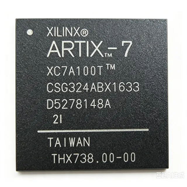
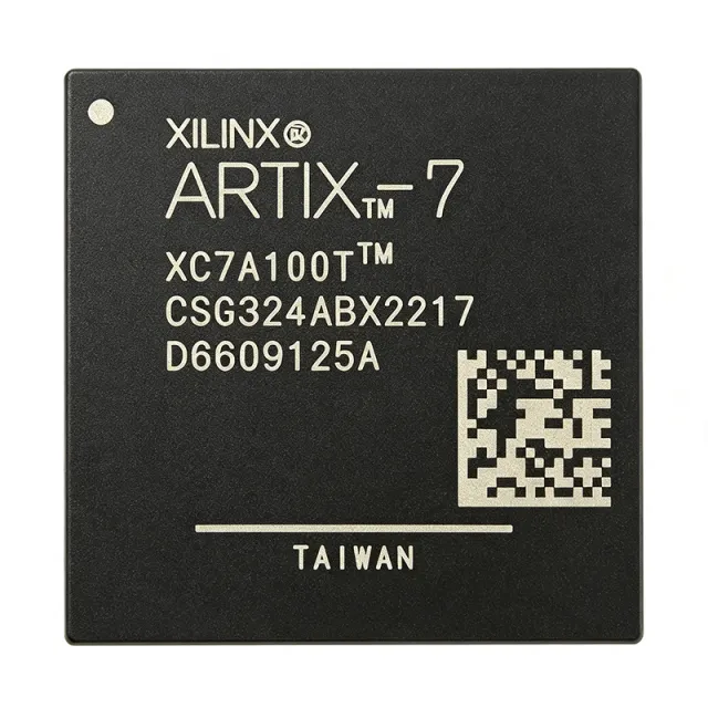
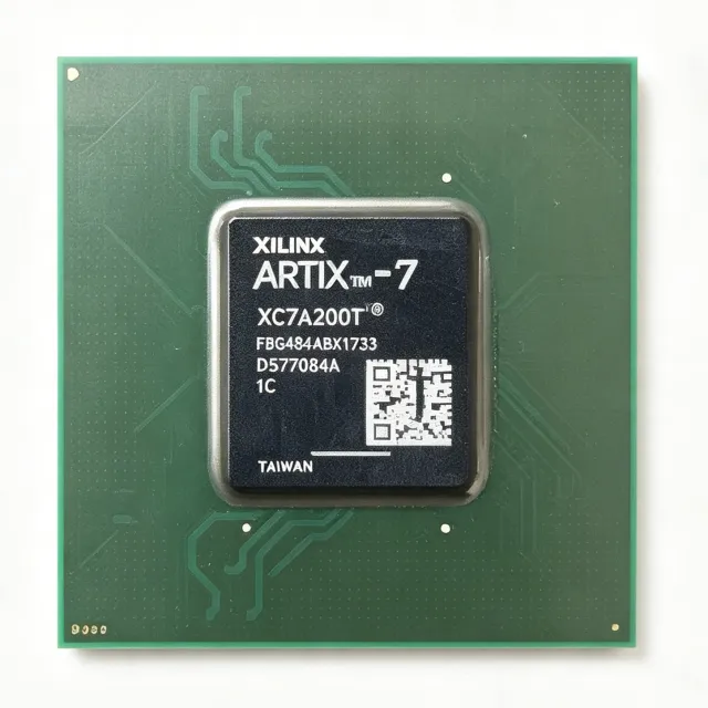
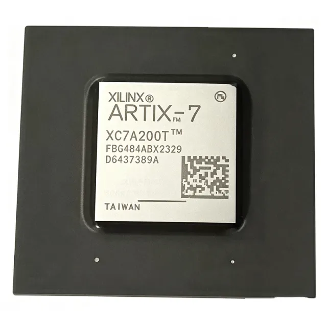
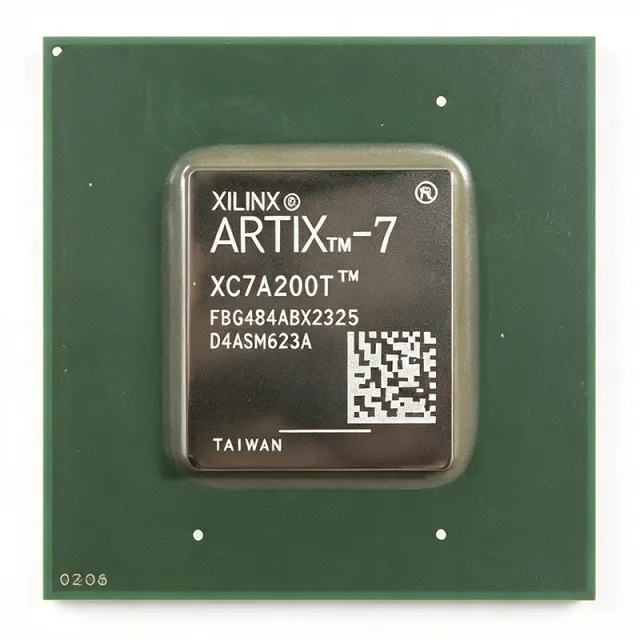
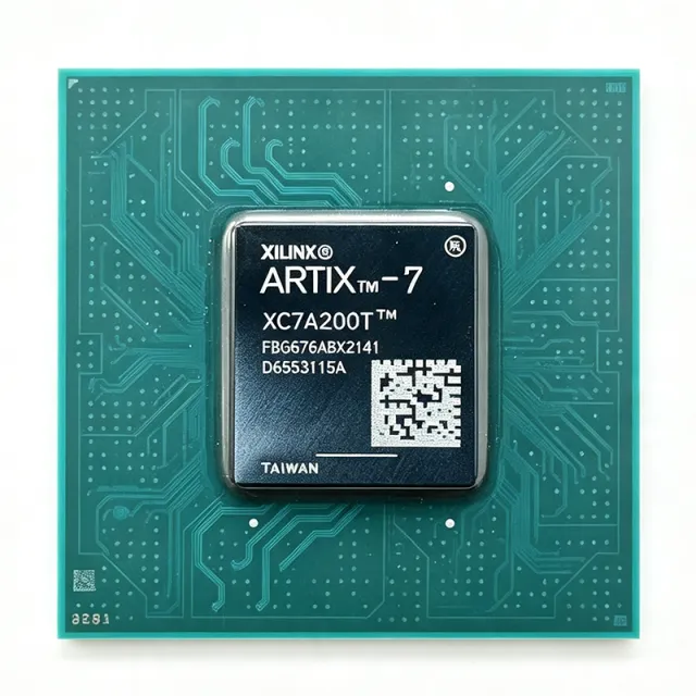
The AMD XC7A12T-1CSG325I is an Artix-7 field-programmable gate array with 12,800 logic cells, 150 I/O, and 28 nm fabrication technology in a 325-pin CSBGA package. The verified distributor data also identifies 737,280 as an associated device figure and lists a 1 V core supply value. These figures position the device as a compact FPGA platform for embedded control, industrial automation, communications, instrumentation, and cost-sensitive designs that require programmable logic and a substantial pin count.
A field-programmable gate array is a semiconductor whose digital logic, memory, and I/O behavior can be configured after manufacture. Within the product hierarchy, an FPGA is a programmable-logic device and a semiconductor. The Artix-7 family combines programmable logic resources with a relatively compact package, allowing engineers to consolidate functions that might otherwise require separate processors, glue logic, and interface devices. The XC7A12T-1CSG325I specifically uses a CSBGA package with 324-LFBGA/CSPBGA notation in the verified distributor listings.
The principal verified attributes are the 12,800-cell Artix-7 logic capacity, 150 available I/O, 28 nm process technology, 1 V value, and 325-pin package. The 150-I/O count is particularly useful for parallel data acquisition, multiple external memory interfaces, control signals, and high-pin-count communication peripherals. The large BGA land pattern also supports dense routing in multilayer PCB designs, but it requires careful escape routing, via planning, and assembly-process control.
This is an FPGA rather than a fixed-function microcontroller, so the implemented design is defined by the bitstream loaded into the device. That architecture allows logic behavior to be revised without changing the PCB when requirements evolve. It also makes configuration memory, startup sequencing, clocking, decoupling, and I/O standards central engineering considerations. Exact block counts, memory resources, supported interfaces, performance grades, power limits, and electrical characteristics beyond the supplied verified values require the AMD device documentation before design release.
Typical uses include industrial factory automation, industrial motor and motion control, network-interface equipment, test and measurement systems, embedded instrumentation, and compact communications platforms. In these applications, the 150 I/O and 12,800 logic cells can consolidate parallel control, acquisition, protocol, and data-processing functions, while the Artix-7 device family provides a path to hardware specialization and field updates.
PCB planning should prioritize the BGA escape path, layer transitions, clean power distribution, and thermal spreading around the device. Because the verified package is not represented by an available canonical SVG package key, the pinout is not reproduced here. Engineers should use the official AMD Artix-7 package pinout files to verify every ball assignment, power pin, configuration pin, and keep-out region before layout release.
This page consolidates verified distributor specifications, package information, sourcing links, comparison fields, and engineering cautions for XC7A12T-1CSG325I. It separates documented values from unavailable technical data and avoids presenting unverified performance, pricing, pin assignments, compliance claims, or replacement parts as established facts.
RFC
Hubungi kami