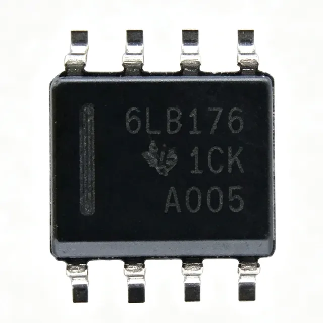
SN74AC241N
SN74AC241N - 8-Channel 3-State Buffer | Texas Instruments
Texas Instruments SN74AC241N is an eight-channel, non-inverting CMOS buffer with independently controlled 3-state outputs, a 2 V to 6 V operating supply range, and a 20-pin PDIP package. The device is organized as two 4-bit buffer elements and is intended for bus-oriented receivers, transmitters, memory-address drivers, and clock-driver applications. According to the TI product page, the SN74AC241 family supports a -40 °C to 85 °C operating-temperature range for the N package.
A logic buffer is a digital semiconductor that reproduces an input signal at an output while providing buffering between a source and the next circuit stage. The 74AC family belongs to the advanced CMOS logic hierarchy, combining low-power operation with balanced drive capability and relatively high input impedance. In the SN74AC241, the tri-state output function allows each group of four outputs to be placed in a high-impedance state, preventing a disabled driver from actively driving a shared bus.
The principal feature is independent output-enable control, allowing two 4-bit sections to be enabled or disabled separately. The non-inverting architecture preserves input logic polarity. Operation from 2 V to 6 V supports both 3.3 V and 5 V systems, while the maximum input voltage of 6 V provides tolerance for supply-transient conditions. The exact propagation-delay, output-current, input-current, and static-power values are not stated in the retrieved product information and must be confirmed in the manufacturer datasheet before timing, fanout, or signal-integrity calculations.
SN74AC241N is a bus-oriented octal buffer rather than a general-purpose open-collector transceiver. Unlike a bidirectional transceiver, its data paths are unidirectional, and unlike a conventional non-3-state buffer, each four-output bank can be disabled. This makes the device appropriate when a controller, memory interface, or peripheral must be isolated from a shared bus while preserving standard logic levels. The N suffix identifies the through-hole PDIP package; board layout, insertion, and rework requirements therefore differ from surface-mount alternatives.
Typical uses include address-line buffering between a memory controller and external memory, clock distribution into bus loads, isolation of peripherals from shared data buses, and buffering of control signals in modular industrial equipment. Because the device supports 3-state outputs, firmware or external logic can determine which bank drives a shared bus. Designers should still verify timing against the worst-case load and trace capacitance shown in the manufacturer datasheet rather than assuming performance from the family name alone.
Decoupling and signal-integrity practice remain important in high-speed systems. Place the supply bypass capacitor close to the device, provide a continuous return path for output-current transients, and keep enable traces away from sensitive analog paths. Do not enable a bank while two outputs contend on the same bus unless the downstream system explicitly supports bus contention. Confirm that the selected source and destination devices meet the AC family voltage, temperature, and timing limits before using the buffer as an interface between unrelated logic families.
This product page combines the manufacturer ordering information with practical bus-isolation guidance, verified package details, and a parameter-by-parameter replacement comparison. It also highlights the distinctions that matter during PCB design: the PDIP-20 footprint, independent 3-state enable control, unidirectional non-inverting operation, and the need to validate exact timing and drive-current limits against the selected system load.
RFC
Hubungi kami