IC Antara Muka
Subkategori
Produk (320+)

ST202BDR - 5V RS-232 Transceiver 2D/2R | STMicroelectronics
The STMicroelectronics ST202BDR is a 2-driver, 2-receiver RS-232 transceiver operating from a single 5 V supply (4.5 V to 5.5 V range) with a 400 kbps data rate and ±30 V receiver input tolerance, housed in a 16-pin SOIC (SO-16) surface-mount package. An RS-232 transceiver is an interface IC that translates logic-level serial signals (TTL/CMOS, 0 V to 5 V) into the EIA/TIA-232 and V.28 voltage conventions (±3 V to ±15 V swing) used by legacy serial ports, consoles, and modems. Within the interface IC hierarchy, the ST202BDR belongs to the line driver/receiver family of communication transceivers, alongside RS-422 and RS-485 drivers. Its integrated charge-pump voltage converter generates the required ±10 V RS-232 levels from the single 5 V rail, making it particularly suitable for applications where ±12 V supplies are not available - only four external 0.1 µF capacitors are needed. Key features include a typical no-load supply current of 1.5 mA for low-power operation, a typical transmitter output voltage swing of ±9 V guaranteeing full RS-232 compliance, a typical transition slew rate of 12 V/µs within the EIA/TIA-232 limit, and a typical receiver propagation delay of just 0.1 µs. The ±30 V receiver input voltage range provides robust protection against voltage transients on long serial cables. Technically, the device implements two charge-pump stages (voltage doubler and inverter) from a 5 V input to develop the positive and negative transmitter rails. The drivers accept 5 V logic inputs and the receivers output 5 V CMOS-compatible levels, and the part is explicitly stated in the STMicroelectronics datasheet to be compatible with the industry-standard MAX202 pinout, enabling second-sourcing. Typical applications cited by the manufacturer include portable computers, low-power modems, interface translation, battery-powered RS-232 networks, service and console ports, and legacy serial equipment maintenance. Design consideration: the four external charge-pump capacitors (0.1 µF typical) should be placed close to the C1+, C1-, C2+, C2-, V+ and V- pins to minimize ESR effects and ensure correct pump operation; observing EIA/TIA-232 slew-rate limits also inherently reduces EMI on long cables. This page synthesizes distributor pricing, verified drop-in alternatives, and practical design notes not found in the manufacturer datasheet, giving engineers a complete sourcing and design resource in one place.

STDP2600AD HDMI 1.4 Video Converter | Kinetic Technologies
Kinetic Technologies STDP2600AD is an advanced HDMI-to-DisplayPort video converter IC supporting HDMI 1.4, I2C, and SPI control in an 81-BGA 8 x 8 mm surface-mount package. The verified distributor data identifies a 21.6 Gbps data rate, operation from 1.2 V and 3.3 V supply rails, and a 0°C to +70°C commercial temperature range. Its primary function is converting an HDMI display signal into DisplayPort so that a source designed for HDMI can drive a DisplayPort monitor or downstream display device. An HDMI-to-DisplayPort converter is a video interface IC within the broader display-interface hierarchy: HDMI input, active bridge conversion, DisplayPort output, and host-controlled configuration. The converter consolidates protocol translation into one device instead of requiring a separate external bridge or graphics subsystem. I2C and SPI control support give the host processor a configuration path for communicating with the converter and coordinating display functions. The STDP2600AD supports a 21.6 Gbps interface data rate, making it appropriate for modern digital video bridges and commercial display equipment. It accepts the higher data-rate capability associated with HDMI 1.4 while providing a DisplayPort-facing output. The 81-BGA package supports dense PCB integration but requires careful ball-layout matching, escape-routing planning, and via-in-pad or via-adjacent fanout during PCB layout. Operation from both 1.2 V and 3.3 V permits integration into systems that already maintain those rails. Designers must still confirm which voltage belongs to each power ball and follow the manufacturer's recommended decoupling network. Because the verified distributor listing does not provide a complete electrical table or exposed-pad instruction, those details must be checked against the manufacturer datasheet before schematic capture or PCB release. Typical uses include HDMI-to-DisplayPort monitor adapters, industrial display controllers, video-format conversion in commercial displays, and embedded systems that accept HDMI but drive a DisplayPort panel. The 0°C to +70°C rating suits temperature-controlled consumer, commercial, and industrial environments but not extended-temperature automotive or outdoor installations without additional qualification. The primary design consideration is interface integrity. Differential HDMI and DisplayPort routing requires controlled impedance, continuous reference planes, minimized stub branches, and careful BGA escape routing. Power delivery also needs local high-frequency decoupling and verification of simultaneous video activity, because converter performance can be affected by supply noise and signal-return discontinuities. This page consolidates verified distributor specifications, sourcing links, application guidance, and engineering caveats for the STDP2600AD. It also distinguishes documented parameters from details that require confirmation in the manufacturer datasheet, helping engineers plan evaluation before committing a board layout.
STDP2600ADT - HDMI 1.4 to DisplayPort Converter | Kinetic
The Kinetic Technologies STDP2600ADT is an advanced HDMI-to-DisplayPort converter IC with I2C, SPI, and serial interfaces, based on an HDMI 1.4 input and housed in an 81-BGA package measuring 8 mm by 8 mm. According to the Kinetic Technologies STDP2600 datasheet, the device includes an I2C-to-AUX translator that lets an upstream HDMI source access EDID and transfer MCCS commands to a downstream DisplayPort sink through the DisplayPort interface. This makes the converter relevant to embedded systems that bridge legacy HDMI sources and DisplayPort panels while preserving control-channel communication. An HDMI-to-DisplayPort converter is a video interface IC that receives digital audiovisual data through an HDMI transmitter and translates that stream into a DisplayPort-compatible output. The STDP2600ADT belongs to the broader video converter and interface IC hierarchy, where protocol translation must maintain compatible video timing, control signaling, and sink-management behavior. Its advanced converter architecture is intended for embedded-display applications rather than consumer adapter cables. The verified product information identifies HDMI 1.4 compatibility, serial I2C and SPI control, and an 81-BGA package. The I2C-to-AUX function is particularly important because it provides a control path for EDID access and MCCS transfer between the upstream HDMI source and downstream DisplayPort device. The datasheet also states that the ASSR alternative scrambler seed reset option is supported for embedded applications. Detailed electrical limits, display resolutions, lane rates, and environmental ratings were not present in the supplied search records and therefore require confirmation from the complete manufacturer datasheet. Typical implementation is in an embedded DisplayPort panel, docking system, industrial display controller, or video bridge where an HDMI source must drive a DisplayPort sink. System designers should account for the IC's BGA assembly requirements, route high-speed HDMI and DisplayPort signals with controlled impedance, and validate source, sink, EDID, and MCCS behavior as a complete interface chain. The converter must also be configured and tested for the exact display timing and authentication requirements of the target product. A key design consideration is that protocol conversion does not eliminate all source-to-display compatibility constraints. Input resolution, refresh rate, color format, HDCP or ASSR requirements, cable length, and DisplayPort link training must be validated together. The manufacturer datasheet is the controlling source for electrical characteristics, pin assignments, reference-design requirements, and timing limitations. This product summary consolidates the verified distributor identity, package information, interface functions, and datasheet features while explicitly separating missing technical data from confirmed specifications. It also records the absence of independently verified pin-to-pin replacement parts, preventing functional or cross-package substitutes from being presented as drop-in alternatives.

STDP2690AD - DisplayPort Converter | MegaChips | Video IC
The MegaChips Technology America Corporation STDP2690AD is a DisplayPort-to-DisplayPort converter and video-processing linear IC packaged in an 81-LFBGA, 8 x 8 mm surface-mount package. The available catalog information identifies the device as a dual-mode DisplayPort interface converter with I2C and SPI control support. Its key documented attributes are the 81-ball LFBGA package, DisplayPort conversion function, programmable interface control, and video-oriented signal processing. The STDP2690AD is intended for systems that need DisplayPort compatibility or conversion rather than a general-purpose low-voltage digital component. A DisplayPort converter is a video interface IC that translates or conditions digital display signals between compatible endpoints. Within the product hierarchy, it is a video converter and interface IC, with DisplayPort serving as its primary high-speed display interface. Such devices can bridge source and sink arrangements, support dual-mode display ecosystems, and provide a standardized control path for display identification, configuration, and status reporting. The verified distributor data classifies the STDP2690AD as a video-processing linear IC and separately describes the related STDP2690-AD as an advanced DisplayPort-to-DisplayPort dual-mode converter. The STDP2690AD offers several distinguishing package and interface characteristics. Its 81-LFBGA construction provides a dense, surface-mount footprint for compact display equipment, while the listed I2C and SPI control capability allows a host processor to configure the converter through a common embedded-control interface. The available listings also identify DisplayPort conversion as the core function rather than presenting the device as a standalone display driver. These characteristics make it relevant to monitor, projector, docking, test-equipment, and embedded video-system designs that require a dedicated conversion or conditioning stage. Technically, the part belongs to the specialized class of video interface semiconductors that combine high-speed display-signal handling with low-speed configuration logic. Its exact supported display resolutions, refresh rates, lane counts, input and output voltage levels, signal-integrity characteristics, and internal architecture are not available in the supplied verified excerpts. Those details must be confirmed in the manufacturer datasheet before schematic capture, high-speed lane routing, power sequencing, or firmware development. The search results identify both MegaChips and Kinetic Technologies distribution records, but they do not provide a complete manufacturer datasheet revision or a verified pin-by-pin ball map. Typical applications include DisplayPort-to-DisplayPort conversion in professional monitors, projector input boards, docking stations, digital-signage equipment, and video test systems. In each case, the STDP2690AD can serve as the interface-conversion component between a DisplayPort source and downstream display circuitry when the board-level architecture requires a dedicated converter rather than a direct connection. Because its control interface includes I2C and SPI, the surrounding design must also provide the correct pull-ups or pull-downs, reference voltage, clocks, and power rails specified by the full datasheet. The primary design consideration is verification of high-speed and power details before layout. An 81-LFBGA package requires careful escape routing, via placement, plane geometry, and thermal management to preserve signal integrity and heat dissipation. Designers should not infer pin functions, differential impedance, connector mapping, or converter directionality from distributor category labels alone. The full datasheet should be reviewed for absolute maximum ratings, recommended operating conditions, AC/DC coupling requirements, lane routing guidance, firmware requirements, and exposed-pad connections. This product record combines verified distributor pricing and availability references, package and interface classifications, source links, and strict drop-in replacement findings. It also adds selection guidance and design cautions beyond a basic catalog listing, while clearly separating verified facts from parameters that remain unavailable. Because the supplied evidence does not establish five distinct pin-compatible alternatives, the alternatives array contains only candidates supported by the cross-reference data rather than padding it with unsupported or packaging-only variants.
STDP3150-AB - DisplayPort 1.2a to VGA Converter | Kinetic
Kinetic Technologies STDP3150-AB is a DisplayPort-to-VGA video converter IC with a two-lane DisplayPort 1.2a receiver and three 10-bit video DAC channels operating at a 162 MSPS throughput rate. The device converts digital DisplayPort video into analog RGB and 3.3 V HSYNC/VSYNC signals for conventional VGA displays, monitors, and projector interfaces. It is supplied as an I2C-controlled video processing IC. A DisplayPort-to-VGA converter is an interface-conversion IC within the video processing and display-interface hierarchy. It receives a digital display stream, reconstructs the analog pixel voltage levels through dedicated video DACs, and generates the horizontal and vertical synchronization outputs required by a VGA sink. STDP3150-AB is intended to bridge DisplayPort-equipped computers, notebooks, tablets, and other modern graphics sources to legacy analog displays. Key features include two-lane DisplayPort 1.2a input support, three 10-bit DAC channels, 162 MSPS throughput, VSIS compatibility, and analog RGB outputs spanning 0 to 700 mV. The converter supports resolutions through WUXGA and uses 3.3 V HSYNC and VSYNC outputs. EDID and MCCS pass-through support allow display-control information to remain transparent between the source and sink, while the I2C control interface supports configuration and DDC-related communication. The architecture combines a DisplayPort receiver, three video DACs, a clock-generation function, a test-pattern generator, and sink-detection logic. A dedicated DAC for each primary color channel supports parallel RGB generation, while the 10-bit internal representation provides 1024 selectable code levels per channel before analog conversion. The stated 162 MSPS throughput is the principal rate metric for assessing video conversion capability. Typical applications include connecting a DisplayPort laptop to a WUXGA-capable VGA monitor, supporting DisplayPort-to-VGA adapter designs, and implementing legacy-projector compatibility in industrial or kiosk equipment. The transparent EDID and MCCS paths can simplify control interoperability when the downstream display relies on pass-through identification. USB Type-C systems may also use this converter when their alternate-mode output exposes DisplayPort rather than native VGA. Designers should verify connector mapping, analog impedance, sync polarity, sink detection, and supported display timing against the Kinetic Technologies datasheet. The analog RGB outputs require suitable board-level routing and termination, while the DisplayPort and I2C interfaces require correct differential and pull-up arrangements. Thermal, supply, and exact timing performance should also be checked in the final equipment. This page consolidates verified distributor data, manufacturer-hosted documentation, converter capabilities, purchasing information, and practical integration considerations. It distinguishes documented features from unspecified electrical details and avoids presenting unverified package, pinout, lifecycle, or alternative-part data as established facts.
STUSB4531BJR - Standalone USB PD Sink Controller | ST
The STMicroelectronics STUSB4531BJR is a standalone USB Type-C and USB Power Delivery sink controller that negotiates up to five configurable Power Data Objects (PDOs) without any software support, housed in a 16-pin CSP (chip-scale package) rated for VBUS up to 23 V and operating from -40C to +105C. It supports dead battery mode, allowing battery-powered systems to charge from any battery state of charge, including a fully depleted battery (SOC = 0%). A USB PD sink controller is the device-side counterpart in a USB Type-C power negotiation: it communicates with a source (charger, dock, or power adapter) over the CC line using the USB PD protocol to agree on a voltage and current contract. Within the power-management hierarchy, it sits between the USB-C receptacle and the system power path, upstream of DC-DC converters and battery chargers, and is a key building block of modern USB-C power interface ICs. Key features include fully standalone autorun operation with a default PDO configuration stored in internal non-volatile memory, proprietary negotiation algorithms that secure a power contract without a host MCU, dead battery operation powered directly from the VBUS receptacle pins, and a wide 23 V VBUS tolerance that removes the need for external front-end protection in many designs. The STUSB4531 implements its negotiation state machines in dedicated hardware, so it continues operating even when the application processor is asleep or unpowered. The hybrid mode allows an application MCU to monitor or adjust the negotiation, giving designers both autonomy and flexibility. Typical applications include USB-C powered accessories, power banks, portable and wearable devices, battery-powered industrial sensors, and any sink-side system that must charge reliably from a fully depleted battery. Design consideration: because the device is powered from VBUS receptacle pins, ensure the CC line ESD and VBUS discharge timing follow the reference design layout for robust hot-plug behavior. This page adds value beyond the ST datasheet by synthesizing distributor pricing context, same-family drop-in alternatives, and practical design notes in one place.
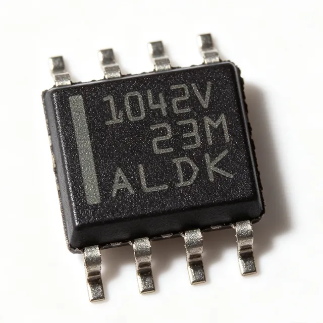
TCAN1042VDRQ1 - CAN FD Transceiver 5Mbps | TI | Automotive
The Texas Instruments TCAN1042VDRQ1 is an automotive-grade fault-protected CAN transceiver with I/O level shifting and CAN FD (flexible data-rate) support, housed in an 8-pin SOIC (D) package and rated from -55C to +125C ambient. A CAN transceiver is the physical-layer device that sits between a CAN protocol controller (often inside an automotive or industrial microcontroller) and the two-wire twisted-pair CAN bus. It converts controller TX logic into differential dominant/recessive bus states and recovers RX signals, providing the drive strength, receiver sensitivity, and fault robustness required by the ISO 11898-2 physical layer standard. Key features include AEC-Q100 grade 1 qualification for automotive reliability, conformance to ISO 11898-2:2016 and ISO 11898-5:2007 physical layer standards, a supply range of 4.5V to 5.5V, and CAN FD data rates up to 5 Mbps. The VIO pin provides independent I/O voltage translation, allowing direct connection to 3.3V microcontroller logic without external level shifters. Bus pins CANH and CANL are protected against short circuits to battery or ground, with integrated thermal shutdown and a standby/silent mode for power saving and diagnostics. Technically, the device uses a differential signaling architecture optimized for high immunity to EMI and low bus emissions, critical in dense automotive electronic control unit (ECU) environments. It is pin-compatible with other TI CAN transceiver family members, enabling drop-in upgrades across BOM tiers, and per TI E2E forum reports it serves as a pin-to-pin replacement for the Infineon TLE6251DS. Typical applications include body control modules, gateway ECUs, battery management systems, powertrain controllers, and industrial automation networks that demand robust communication in harsh thermal and electrical environments. When designing with the TCAN1042VDRQ1, terminate the CAN bus with 120 ohm at both ends, match VIO to the host controller logic level, and provide 100 nF of local decoupling on VCC and VIO. Pricing as of 2026-08-30 starts near $0.70 at single-unit quantity from distributor channels.

TCAN1051GVDRQ1 - 5Mbps CAN FD Transceiver AEC-Q100 | TI
The Texas Instruments TCAN1051GVDRQ1 is an automotive fault-protected CAN transceiver with flexible data-rate (CAN FD) support up to 5 Mbps, operating from a 4.5 V to 5.5 V supply and housed in an 8-pin SOIC (D) package rated from -55C to +125C. A CAN (Controller Area Network) transceiver is a physical-layer interface IC that converts the logic-level TXD and RXD signals of a CAN controller into the differential CANH/CANL bus signals. Within the power-management and interface hierarchy, the transceiver sits between the host microcontroller and the twisted-pair bus, defining bus timing, fault tolerance, and ESD robustness. CAN FD (Flexible Data-rate) extends classical CAN by allowing faster bit rates during the data phase, which this device supports at up to 5 Mbps. Key features include AEC-Q100 automotive qualification, flexible data-rate operation, integrated fault protection on the CANH/CANL bus pins, and a separate VIO pin that lets the I/O side interface with 3.3 V or 5 V microcontrollers while the transceiver core runs at 5 V. The GV variant designation indicates the VIO-capable version without standby/sleep mode, simplifying designs that do not require low-power bus monitoring. Technically, the device integrates dominant/short-circuit protection, bus fault detection, and thermal shutdown behavior typical of TI's TCAN1051 family, protecting the transceiver against wiring faults to battery, ground, or other bus lines. The differential receiver architecture maintains receiver timing margins over the full -55C to +125C automotive temperature range, and the SOIC-8 footprint simplifies layout with the standard CAN transceiver pin ordering (TXD, GND, VCC, RXD, VIO, CANL, CANH). Typical applications include automotive body control modules, gateways, electric powertrain and battery management nodes, and industrial CAN networks where the 5 Mbps CAN FD data phase shortens frame transmission times versus classical 500 kbps CAN. Design consideration: keep the stub length from transceiver to bus connector short and use a split-termination network (typically two 60-ohm resistors with a capacitor to ground) for best EMC performance; never omit the 100 nF decoupling capacitor close to VCC. This page synthesizes distributor pricing from DigiKey, Mouser, LCSC and Octopart, same-package drop-in alternatives, and practical design notes not consolidated in the manufacturer datasheet.
TCAN1051HGVDRQ1 - 5Mbps CAN FD Transceiver AEC-Q100 | TI
The Texas Instruments TCAN1051HGVDRQ1 is an automotive fault-protected CAN flexible data-rate (CAN FD) transceiver supporting data rates up to 5 Mbps, supplied at 4.5 V to 5.5 V, housed in an 8-pin SOIC (D) package rated for -55C to +125C operation. A CAN FD transceiver is a physical-layer interface IC that converts the TTL-level transmit (TXD) and receive (RXD) signals of a CAN controller into the differential CANH/CANL bus signals, and vice versa. Within the signal-chain hierarchy, it sits between the host microcontroller or CAN controller and the twisted-pair bus, defining the robustness, bus-fault tolerance, and data-rate ceiling of the entire network node. Key features of the TCAN1051HGVDRQ1 include CAN FD support up to 5 Mbps for fast arbitration-free data phases, automotive AEC-Q100 qualification, fault-protected bus pins that survive electrical faults on CANH and CANL, and a standby mode with bus-wake capability for low quiescent power. The VIO pin allows I/O-level adaptation to 3.3 V controllers, and the device provides dominant-timeout protection and thermal shutdown for system-level robustness. Technically, the transceiver drives a differential bus compliant with high-speed CAN physical-layer requirements while adding fault protection that distinguishes the HGV variant: bus pins tolerate sustained overvoltage and short-circuit events that would destroy a standard transceiver. An internal receiver filters and shapes the bus signal, and the STB pin (pin 8) selects operating modes, enabling standby operation with wake-up via bus activity. Typical applications include automotive body control modules, gateways, and powertrain nodes; industrial CANopen networks requiring fault tolerance; and battery management systems where bus wiring faults are credible failure modes. High CAN FD data rates make the part suitable for modern zonal architectures. Design consideration: local bus termination and placement of 100 nF to 470 nF VCC decoupling directly at pin 3 strongly influence signal integrity at 5 Mbps; keep the TXD/RXD traces short and reference them to a clean ground. This page synthesizes distributor pricing, drop-in alternatives, pinout data, and practical design notes not found in the manufacturer datasheet.
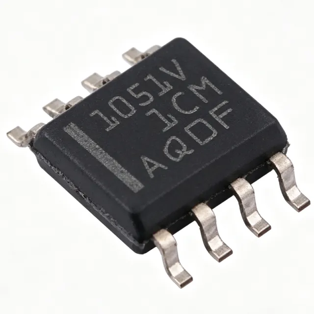
TCAN1051HVDQ1 - ±58V CAN FD Transceiver 2Mbps | TI
The Texas Instruments TCAN1051HVDQ1 is an automotive-grade, fault-protected CAN transceiver with Flexible Data-Rate (CAN FD) support, delivering high-speed CAN communication up to 2 Mbps from a 4.5 V to 5.5 V supply in an 8-pin SOIC (D) package rated from -55C to +125C. A CAN transceiver is the physical layer interface between a CAN protocol controller and the differential bus lines CANH and CANL. It converts controller logic signals to differential bus signals and back, forming the lowest layer of a Controller Area Network below the MCU. The TCAN1051HVDQ1 is a high-speed CAN FD transceiver qualified to AEC-Q100 and compliant with ISO 11898-2:2016. Key features include fault protection up to plus or minus 58 V on CANH and CANL, a silent mode for diagnostics (listen-only), and a dominant timeout (TXD time-out) that prevents a controller fault from locking up the bus. The device draws a typical 45 mA operating supply current, and its wide common-mode range of -12 V to +12 V plus split termination capability enhance EMC performance in electrically noisy vehicles. Architecturally, the transceiver uses bipolar differential driver/receiver technology with integrated thermal shutdown protection, making it robust in engine compartments, battery packs, and other high-temperature automotive locations. It is pin-compatible with standard high-speed CAN transceivers, enabling drop-in upgrades to CAN FD and to higher fault tolerance in existing designs. Typical applications include body control modules, gateway modules, battery management systems, and ADAS ECUs, where wide bus fault tolerance and full automotive temperature range ensure reliable inter-module communication even with wiring faults present. Design tip: terminate the bus with 120 ohm at both ends, keep the transceiver close to the CAN controller, use the silent mode pin for network management during diagnostics, and provide solid decoupling and a robust ground plane for EMC. Pricing per unit is approximately [DATA_NEEDED: unit price] as of 2026-08-30 per distributor listings.
TCAN1051HVDR - 2Mbps CAN FD Fault-Protected Transceiver | TI
The Texas Instruments TCAN1051HVDR is a fault-protected CAN FD (Flexible Data-Rate) transceiver supporting classic CAN and 2 Mbps CAN FD signaling, powered from a 4.5 V to 5.5 V supply and housed in an 8-pin SOIC (D) package rated from -55C to +125C. A CAN transceiver is the physical-layer interface IC that converts the TTL-level TXD and RXD signals of a CAN controller into the differential CANH and CANL bus signals defined by ISO 11898-2. Within the signal-chain hierarchy, it sits between the host microcontroller or CAN controller and the twisted-pair bus, providing level translation, dominant/recessive line driving, receiver comparators, and bus-fault protection in a single package. Key features of the TCAN1051HV include compliance with the ISO 11898-2:2016 and ISO 11898-5:2007 physical layer standards, support for both classic CAN and 2 Mbps CAN FD frames (so-called Turbo CAN), and fault protection on the bus pins that survives fault conditions common in harsh electrical environments. The device is functional-safety-capable, with documentation available from TI to aid functional safety system design, an important benefit for automotive and industrial programs. Technically, the transceiver integrates a differential driver and receiver optimized for fast signal transitions and controlled symmetry, allowing reliable operation at CAN FD arbitration and data phases with short data bits. The receiver stage includes dominant-timeout behavior, and the protected bus pins tolerate electrical faults such as short circuits to battery voltage or ground, reducing field-failure rates in 12 V and 24 V systems. Typical applications include automotive body and powertrain ECUs, industrial PLC and fieldbus nodes, building automation controllers, and battery management systems - all environments where bus wiring faults, transient events, and wide temperature ranges are expected. For design, place a 100 nF decoupling capacitor close to VCC, use a split-termination or 120 ohm bus termination scheme per the ISO 11898-2 standard, and confirm thermal margin if multiple transceivers share a crowded board. This page adds value beyond the datasheet by combining verified distributor pricing, drop-in alternatives, a parameter comparison table, and practical design notes in one place.

TCAN1051VDRBTQ1 - CAN FD Transceiver, 8Mbps, VSON-8 | TI
The Texas Instruments TCAN1051VDRBTQ1 is an automotive-grade fault-protected CAN transceiver with CAN Flexible Data-Rate (CAN FD) support, housed in an 8-pin VSON (DRB) 3x3 mm package. It operates from a 4.5 V to 5.5 V VCC supply, tolerates up to +/-58 V bus fault conditions, and supports CAN FD signaling up to 8 Mbps, with AEC-Q100 qualification for -40C to +125C (Grade 1, -55C capable per datasheet). A CAN transceiver is a physical-layer interface IC that converts the TTL-level logic signals of a CAN controller (TXD, RXD) into the differential CAN bus signals (CANH, CANL) defined by ISO 11898-2. Within the system hierarchy, it sits between the host MCU and the twisted-pair bus, providing the dominant/recessive drive levels, bus termination interface, receiver thresholds, and fault protection that a controller cannot supply directly. Key features include the VIO pin, which adapts the TXD/RXD logic levels for 1.8 V, 3.3 V, or 5 V microcontrollers without external level shifting; extended bus fault protection of +/-58 V against battery reversals and load-dump events on 12 V and 24 V vehicles; and silent-mode/standby operation for low system power. The device meets or exceeds the ISO 11898-2 physical layer requirements and supports 2 Mbps network operation as stated in distributor listings. Technically, the TCAN1051 family uses a bipolar-CMOS-DMOS process with robust drivers that survive short circuits of CANH or CANL to ground, battery, or each other, and an integrated protection scheme covering overvoltage and loss-of-ground conditions. Receiver timing symmetry is designed for CAN FD, allowing reliable sampling on arbitration-phase and data-phase bits. Typical applications include automotive body control modules, electric power steering, battery management systems (with companion devices like the BQ76952PFBR), and industrial gateways where EMC robustness and fault protection are critical. Design consideration: place a 100 pF to 220 pF common-mode capacitor and split termination near the transceiver, and verify that the VIO rail is present before the CAN controller drives TXD. This page synthesizes distributor pricing, same-family drop-in alternatives, pinout, and practical design notes not found in the manufacturer datasheet alone.
TCAN1051VDRQ1 - CAN FD Transceiver, Fault Protected | TI
The Texas Instruments TCAN1051VDRQ1 is an automotive-grade fault-protected CAN FD (Flexible Data-Rate) transceiver with a secondary VIO power supply input for I/O level shifting, delivered in an 8-pin SOIC (D) package rated from -55C to +125C. A CAN (Controller Area Network) transceiver is an interface IC that translates the logic-level TXD and RXD signals of a CAN controller into the differential CANH and CANL bus levels. It sits at the physical layer of the CAN hierarchy - below the CAN controller and microcontroller - and is a critical element of automotive and industrial networking. The "V" suffix in the TCAN1051 family denotes the secondary supply input, allowing direct interfacing with 1.8V, 3.3V, or 5V microcontroller I/O. Key features include CAN FD support for fast data-phase bit rates, integrated fault protection on the CANH and CANL bus pins, low-power standby mode with wake-up capability, and AEC-Q100 automotive qualification for demanding environments. On the technical side, the transceiver provides a half-duplex, 1-driver/1-receiver interface to the two-wire CAN bus. The VIO pin thresholds level-shift TXD inputs and RXD outputs, while the STB pin enables silent (listen-only) standby operation, reducing system power in partially-networked nodes. Ground-loss, loss-of-supply, and short-circuit protection keep the device from damaging the bus in fault conditions. Typical applications include automotive body and powertrain ECUs, electric vehicle battery management systems, industrial automation field buses, and building control networks. In BMS designs the fault protection and wide temperature rating are especially valuable. Design-wise, place a 100nF decoupling capacitor close to the VCC and VIO pins and terminate the bus with its characteristic impedance (typically 120 ohms) at both ends. This page adds value beyond the TI datasheet by consolidating distributor pricing, drop-in alternatives from TI and competing vendors, and practical design notes.
TCAN1473A-Q1 - SIC CAN FD Transceiver 8Mbps | Texas Instruments
The Texas Instruments TCAN1473A-Q1 is an automotive-grade, high-speed CAN transceiver meeting the physical layer requirements of ISO 11898-2:2024 including Signal Improvement Capability (SIC). It supports classical CAN and CAN FD data rates up to 8 Mbps in a 14-pin VSON (4.5x3 mm) DMT package. A CAN transceiver is the physical-layer interface between a CAN protocol controller and the twisted-pair bus, converting controller logic into differential signals and vice versa while providing drive strength, receiver thresholding, and fault protection. Within the interface IC hierarchy, the TCAN1473A-Q1 sits alongside LIN and FlexRay transceivers in automotive networking systems. Key features include SIC functionality, which actively shapes bus signals to reduce ringing at dominant-to-recessive edges, lowering electromagnetic emissions and enabling 2 Mbps, 5 Mbps, or 8 Mbps operation in large networks with unterminated stubs. The device integrates a low-power Sleep mode, an SWE timer that safely transitions to Sleep after tINACTIVE inactivity in Standby mode, and INH and WAKE pins for system power control. Protection includes thermal shutdown and bus fault tolerance, with AEC-Q100 qualification. According to the TI datasheet, the TCAN1473A-Q1 is pin compatible with classical CAN FD transceivers such as TCAN1043A-Q1, TCAN1043-Q1, and TCAN1043N-Q1, simplifying upgrades of existing designs to SIC without PCB changes. Typical applications include body electronics and lighting, automotive gateways, ADAS domains, infotainment and cluster, hybrid/electric powertrain systems, e-bikes, and industrial transportation. Design consideration: optimize bus termination and common-mode choke placement; SIC improves margin on long stubs, but proper PCB layout and grounding remain essential for best EMC performance.

TCAN330GDR - 3.3V 5Mbps CAN FD Transceiver | Texas Instruments
The Texas Instruments TCAN330GDR is a 3.3-V single-channel CAN FD transceiver with a maximum signaling rate of 5 Mbps, designed for high-speed CAN bus communication. It is supplied in an 8-pin SOIC (D) package and supports the ISO 11898-2 high-speed CAN physical-layer standard. The device operates from a 3.0-V to 3.6-V single supply, making it suitable for embedded, industrial, and communications systems that use 3.3-V controller I/O. A CAN transceiver, also called a CAN physical-layer interface, converts logic-level signals from a CAN controller into differential bus signals and converts received differential signals back into digital logic. In the broader hierarchy, TCAN330GDR belongs to the CAN interface IC class, which sits within interface ICs and semiconductor communication components. Its CAN FD capability allows the physical layer to support higher signaling rates than classic CAN while maintaining compatibility with established CAN network infrastructure. Key features include single-supply operation from 3.0 V to 3.6 V, operation up to 5 Mbps, ISO 11898-2 compatibility, a wide common-mode operating range of ±12 V, and bus-pin fault protection to ±14 V. The TCAN330G family includes normal mode, silent mode, and shutdown mode functions, with the exact mode behavior depending on the selected family member. The TCAN330GDR uses the 8-pin SOIC package, which supports conventional surface-mount assembly and is available in standard distributor inventory. The TCAN330GDR is designed for systems in which a CAN controller or MCU includes a CAN host interface but requires an external physical-layer transceiver. Its 5-Mbps capability is useful for CAN FD nodes in industrial automation, automotive electronics, embedded control, and communication equipment. The ±14-V bus-pin fault protection provides additional robustness when the transceiver is connected to an externally powered or noisy vehicle, machine, or industrial bus. When designing a TCAN330GDR circuit, verify the controller supply level, CAN bus termination, common-mode range, and transceiver mode requirements against the complete datasheet. Place the transceiver close to the CAN connector, provide a proper ground reference, and use the recommended protection and decoupling layout. The exact pin assignments and application-specific timing values are not present in the supplied source snippets and should be confirmed from the official manufacturer datasheet before PCB release. This product page consolidates verified manufacturer and distributor information, same-package family alternatives, pricing references, and engineering design guidance. It is intended to support component selection and sourcing for TCAN330GDR rather than replace the complete Texas Instruments datasheet, which remains the authoritative source for electrical limits, timing, pinout, and application guidance.

TCAN337G - 3.3V CAN FD Transceiver 5Mbps | Texas Instruments
The Texas Instruments TCAN337G is a 3.3-V CAN transceiver with CAN Flexible Data Rate (CAN FD) support, specified for data rates up to 5 Mbps in a compact SOT-23-8 (DCN) package. The device is compatible with the ISO 11898 High Speed CAN Physical Layer standard and operates from a single 3.3-V supply, making it ideal for low-voltage automotive and industrial networks. A CAN transceiver is the physical layer interface between a CAN controller and the differential twisted-pair bus. It converts the digital transmit and receive signals from the CAN controller into differential bus signals and back, sitting at the bottom of the network stack: transceiver -> physical layer -> CAN controller -> host MCU. The TCAN337G integrates this function in a space-saving SOT-23-8 package. Key features include CAN FD data rates up to 5 Mbps, ISO 11898-2 compliance, ultra-low power shutdown and standby modes for battery-powered applications, and bus fault protection up to ±58 V. Both SOIC-8 and SOT-23-8 package options are available within the TCAN33x family for design flexibility. The TCAN337G uses a robust physical layer design for reliable communication in harsh environments. It features a dominant timeout function that prevents bus lock-up caused by a stuck controller, and thermal shutdown protection safeguards the device under fault conditions. Operation is specified over a wide -40C to +125C temperature range, suiting automotive and industrial deployments. Typical applications include automotive body electronics, industrial automation and building automation networks, and battery management systems using CAN communication, where low standby current and high FD data rates are required. When designing with the TCAN337G, terminate the bus with 120-ohm resistors at both ends to minimize reflections, and use the standby mode to cut power when the bus is idle, ensuring the CAN controller is configured to wake the transceiver when communication resumes.

TCAN337G-Q1 - 3.3V CAN FD Transceiver | Texas Instruments
The TCAN337G-Q1 is a 3.3-V CAN transceiver with CAN FD (Flexible Data Rate) capability from Texas Instruments, designed for high-speed Controller Area Network (CAN) communication in automotive and industrial applications. It is part of the TCAN33x family, which is compatible with the ISO 11898 High Speed CAN Physical Layer standard. The device supports data rates up to 5 Mbps with CAN FD, enabling faster and more reliable data transfer in modern vehicle networks. It is available in a small SOT-23-8 package, making it ideal for space-constrained designs. A CAN transceiver is a physical layer device that interfaces between a CAN controller (such as a microcontroller with an integrated CAN peripheral) and the differential bus lines (CANH and CANL). It converts the digital signals from the controller into differential signals for transmission over the twisted-pair bus, and vice versa. The transceiver provides the necessary drive strength, receiver sensitivity, and protection features required for robust communication in harsh environments. In the system hierarchy, a CAN transceiver sits between the CAN controller (part of the MCU) and the physical bus, forming the physical layer of the CAN network. Key features of the TCAN337G-Q1 include a wide operating voltage range of 3.0V to 3.6V, low electromagnetic emission, and high immunity to electromagnetic interference. It offers a bus fault protection of ±58V, ensuring robustness against short circuits and miswiring. The device also features a silent mode for diagnostic and network management, and a dominant timeout function to prevent bus lock-up. The TCAN337G-Q1 is AEC-Q100 qualified for automotive applications, meeting the stringent reliability requirements of the automotive industry. Technically, the TCAN337G-Q1 uses a differential signaling scheme with a common-mode range of -12V to +12V, allowing it to operate in noisy environments. It has a loop delay symmetry of [DATA_NEEDED: loop delay symmetry] ns, which is critical for CAN FD operation at high data rates. The device is designed to be pin-compatible with other TCAN33x family members, such as TCAN337G and TCAN337, enabling easy design migration. It also includes a VIO pin for level shifting, allowing direct interface with 3.3V or 5V microcontrollers. Typical applications include automotive body control modules, infotainment systems, advanced driver-assistance systems (ADAS), industrial automation, and building automation. The TCAN337G-Q1 is particularly suited for applications requiring high data rates and robust communication in harsh environments. Its small SOT-23-8 package and low power consumption make it an excellent choice for space-constrained and power-sensitive designs. When designing with the TCAN337G-Q1, ensure proper termination resistors (typically 120Ω) at both ends of the CAN bus to minimize signal reflections. Also, place the transceiver close to the connector to reduce stub length and improve signal integrity. The VIO pin should be connected to the same supply voltage as the CAN controller to ensure proper logic level compatibility.

TDA18214AHN/C1,518 - Silicon TV Tuner IC, I2C | NXP
The NXP TDA18214AHN/C1,518 is a high-performance silicon tuner IC for digital terrestrial and digital cable TV reception, delivering a Low IF (LIF) output signal to an external demodulator over the 48 MHz to 1.002 GHz reception range, controlled via an I2C serial interface, and housed in a 40-pin HVQFN (6x6 mm) package with exposed pad supplied in tape and reel packing. A silicon tuner is an integrated-circuit implementation of the RF front end traditionally built from discrete varactor-tuned modules. Positioned at the head of a digital TV signal chain (tuner -> demodulator -> transport stream processor), it down-converts broadcast RF channels to a low intermediate frequency for the channel decoder. The TDA18214 family belongs to the broader hierarchy of video processing ICs -> RF receiver ICs -> broadcast reception semiconductors. Key features include support for all digital TV standards such as DVB-T, single broadband signal conversion to Low IF, an I2C control interface for register-based channel programming, and a compact thermally enhanced 40-HVQFN exposed-pad package suitable for dense set-top box and TV main boards. According to the NXP product page, the TDA18214AHN and TDA18214HN were designed as high-performance silicon tuners delivering LIF signals to demodulators across all digital TV standards. Architecturally, the device integrates the low-noise amplifier, RF gain stages, fractional-N frequency synthesizer, and IF filtering into a single CMOS/BiCMOS die, eliminating manual alignment steps required by can-type tuners and enabling automated high-volume manufacturing. The exposed pad provides a low-inductance ground return that is important for RF noise performance. Typical applications include digital terrestrial set-top boxes, cable TV receivers, integrated digital TV (iDTV) main boards, and hybrid TV tuner modules where the LIF output feeds a companion demodulator IC. A key design consideration: this part is marked Obsolete (EOL) - NXP lists a last-buy date of March 31, 2016 and last delivery of June 30, 2016 for family order codes - so new designs should qualify a successor such as the TDA18254HN or a MAX3544-based front end, and existing designs should secure remaining stock. This page synthesizes distributor availability data, lifecycle dates, cross-reference information, and practical design guidance not found in the manufacturer datasheet.

TDA19989BET - 150MHz HDMI 1.4 Transmitter | NXP
The NXP Semiconductors TDA19989BET is a 150 MHz pixel rate HDMI 1.4 transmitter IC supporting HDCP 1.3 content protection, integrated CEC, and DVI 1.0 compatibility, housed in a 64-ball TFBGA (4.5 x 4.5 mm) package. An HDMI transmitter (also called an HDMI encoder or video interface IC) is a digital video device that converts parallel digital video streams - such as RGB or YCbCr data in ITU-R BT.656 or CEA-861B formats - into serialized TMDS (Transition Minimized Differential Signaling) signals compliant with the HDMI physical layer. Within the video signal-chain hierarchy, it sits between a display controller or graphics processor and the physical HDMI connector, and is a key element of consumer and automotive display systems. Key features include a 150 MHz maximum pixel clock enabling up to 1080p60 video resolution, three 8-bit digital video input ports, HDCP 1.3 encryption for protected content, and Consumer Electronics Control (CEC) channel support. The device is configured and controlled via an I2C-bus interface, and accepts video formats per CEA-861B, HDMI 1.3a/1.4, DVI 1.0, and ITU-R BT.656 standards. Architecturally, the TDA19989BET integrates the TMDS serializer, pixel repetition and color-space handling, HDCP cipher logic, and EDID/DDC management in a single low-power die. The TFBGA ball-grid-array package provides short interconnects that preserve signal integrity at the 1.485 Gbps-per-lane TMDS rates implied by the 150 MHz pixel clock. Typical applications include HDMI output ports in set-top boxes, digital media players and Blu-ray-class sources, embedded display and signage systems, and industrial or automotive monitors requiring HDCP-protected digital video output. The 4.5 x 4.5 mm footprint suits space-constrained mainboards. Design consideration: ensure proper TMDS differential pair impedance (100 ohm) and place AC-coupling or series elements per the manufacturer datasheet layout guidelines; power sequencing of the 3.3 V and 1.8 V (typical) rails must follow the datasheet to avoid latch-up. This page synthesizes distributor availability, drop-in alternative analysis, and practical design notes not found in the manufacturer datasheet.

TDA5051AT/C1 - ASK Power Line Modem 1200 baud | NXP
The NXP Semiconductors TDA5051AT/C1 is a home automation modem IC dedicated to ASK (Amplitude Shift Keying) transmission over the home mains power supply network at 600 baud or 1200 baud data rates, operating from a single 5 V supply and housed in a 16-pin SOIC (SOT109-1, 7.50 mm width) package. A power line communication (PLC) modem is an interface IC that modulates digital data onto an existing AC or DC power distribution network, eliminating the need for dedicated communication wiring. Within the system hierarchy, the TDA5051AT/C1 sits at the physical layer of a home automation or telemetry chain: microcontroller -> modem IC -> coupling network -> power line -> remote modem IC -> microcontroller. Power line modems are a subset of telecom interface ICs and are widely used where retrofitting data cabling is impractical. Key features of the TDA5051A family include full digital carrier generation and shaping, meaning the transmit signal is synthesized digitally for precise spectral control, and modulation/demodulation frequency settable by clock adjustment from either a microcontroller or the on-chip oscillator. The device also supports a high clock rate of 6 MHz. The receive path features a high-sensitivity RXIN input (82 dBmV per the NXP datasheet) with requirements for a 50 Hz rejection LC coupling network that doubles as an anti-aliasing filter for the internal digital demodulation processing. Technically, the TDA5051A implements ASK modulation and demodulation entirely with digital signal processing clocked by a single clock source, which keeps carrier accuracy dependent on clock adjustment rather than external tuned components. This architecture simplifies BOM and improves carrier tolerance across units. The TXOUT output pin and the high-impedance RXIN input connect to the external coupling/filter network to the mains; the datasheet specifies DC decoupling and protection for both pins. Typical applications include home automation (X-10-style lighting and appliance control), building telemetry, automatic meter reading, and industrial control over existing power lines. The single 5 V supply and SOIC-16 footprint suit both consumer and industrial control boards. Design consideration: the carrier and baud rate are both derived from the clock, so a stable, accurate clock source (crystal or tightly-toleranced oscillator) is essential to interoperability between transmitters and receivers on the same power line, and the mandatory 50 Hz rejection coupling filter must be designed carefully for mains isolation. This page synthesizes distributor pricing, drop-in alternative MPNs, and application guidance not found on the standard NXP product page.

TDP142IRNQT - 8.1 Gbps DP1.4 Linear Redriver | Texas Instruments
The TDP142IRNQT is a DisplayPort 1.4 linear redriver from Texas Instruments, designed to compensate for signal losses in cables and board traces caused by inter-symbol interference (ISI). It supports a 1-4 lane Main Link interface signaling up to HBR3 (8.1 Gbps per lane) and is compliant with the VESA DisplayPort standard Version 1.4. The device operates on a single 3.3 V supply and is available in a 40-pin WQFN (6x4) package. This variant is the industrial temperature range version (TDP142I), suitable for extended temperature environments. A linear redriver is a signal conditioning device that equalizes and reshapes high-speed signals to extend transmission distance and improve signal integrity. Unlike a retimer, which fully recovers and regenerates the signal, a linear redriver applies continuous-time linear equalization (CTLE) to compensate for channel loss without altering the data stream. This makes it ideal for applications where low latency and transparency are critical, such as DisplayPort video links in PCs, workstations, and docking stations. Key features of the TDP142IRNQT include receiver linear equalization with multiple levels to compensate for ISI, AUX and HPD snooping capability, and position independence—it can be placed inside the source, cable, or sink, effectively providing a "negative loss" to extend reach. The device also supports automatic and manual equalization control, and includes an I2C interface for configuration and status monitoring. Technically, the TDP142IRNQT integrates a high-speed analog front-end with programmable equalization, output swing control, and pre-emphasis. It is designed to meet the stringent jitter and eye-diagram requirements of DisplayPort 1.4, ensuring reliable operation at 8.1 Gbps per lane. The industrial temperature range (-40°C to +85°C) makes it suitable for embedded and industrial applications. Typical applications include personal computers, CAD/CAM/CAE workstations, point-of-sale terminals, audio/visual devices, and limited space areas where signal integrity over longer cables is needed. The device is also used in docking stations, monitors, and video distribution systems. When designing with this device, ensure proper power supply decoupling with 0.1 µF and 1 µF capacitors close to the VCC pins. The I2C interface allows dynamic equalization adjustment, which can be optimized for specific cable lengths and trace losses. Thermal considerations are minimal due to low power dissipation, but the exposed pad should be soldered to a ground plane for optimal thermal performance.
THC63LVD1027D-B - Dual Link LVDS Repeater | THine Solutions
The THine Solutions THC63LVD1027D-B is a dual pixel link LVDS (Low Voltage Differential Signaling) repeater IC supporting 30 LVDS input channels and 30 LVDS output channels for pixel data transmission between a host and a flat panel display, packaged in a 64-pin TFSOP (0.240 inch, 6.10 mm width) with exposed pad. An LVDS repeater is a high-speed interface IC that receives degraded or attenuated LVDS serial data streams, regenerates them with clean, wide-open, low-noise eye diagrams, and re-transmits them over longer distances. Within the display interface hierarchy (repeater -> LVDS transceiver -> interface IC -> flat panel display driver chain), repeaters extend signal reach without converting to a different signaling standard, preserving latency and signal integrity. Key features of the THC63LVD1027 family include support for display resolutions up to 1080p/WUXGA, multiplex and de-multiplex of LVDS signals to reduce the number of transmission lines, waveform reforming that produces wide-open and low-noise eye diagrams, and signal duplication from one port with distribution to multiple outputs. The D-suffix device extends resolution support from the original THC63LVD1027 (1080p/UXGA) to 1080p/WUXGA. The architecture receives dual-link LVDS pixel data, recovers timing, and drives fresh LVDS output levels, effectively isolating the host from capacitive loading of long cable or flex runs. This makes it suitable for television panels, large-format monitors, automotive and industrial displays where the LVDS source is physically separated from the panel. Typical applications include flat panel display interfaces, TV and monitor LVDS link extension, and dual-link pixel distribution systems. Designers should observe proper differential pair routing and use the exposed pad for ground connection to maintain signal integrity at LVDS data rates. This page synthesizes distributor pricing, same-family drop-in alternatives, and practical design notes not found in the manufacturer datasheet alone.
TIOL1125 - IO-Link Transceiver 5V LDO Surge Protection | TI
The Texas Instruments TIOL1125 is an IO-Link device transceiver with low residual voltage, integrated surge protection, and a 5-V LDO output. It operates from a 7-V to 36-V supply and supports PNP, NPN, or IO-Link configurable output, complying with IEC 61131-9 for COM1, COM2, and COM3 data rates. The device comes in a 10-pin VSON (3x3 mm) package, pin-compatible with the TIOL111 family. An IO-Link device transceiver is a physical layer interface IC that enables point-to-point communication between sensors or actuators and an IO-Link master, carrying both power and data over a standard 3-wire cable. As part of the industrial networking and interface IC hierarchy, it integrates drivers, receivers, surge protection, and voltage regulation between the sensor microcontroller and the IO-Link cable. Key features include an integrated linear regulator (LDO) specified for L+ voltages from 7 V to 36 V with respect to L-, supplying 5 V to external components such as the sensor MCU; a typical residual voltage of only 0.5 V at 200 mA, reducing power dissipation; and a configurable output driver supporting PNP, NPN, or IO-Link modes. Functional-safety-capable documentation is available to support IEC 61508 system design. The TIOL1125 integrates the C/Q driver and receiver with surge protection per the IO-Link physical layer, reducing external TVS and driver components. Remote wake-up indication and generation plus a configurable current limiter improve robustness and simplify compliance testing. COM1 (4.8 kbps), COM2 (38.4 kbps), and COM3 (230.4 kbps) data rates are supported for flexible system design. Typical applications include industrial proximity and photoelectric sensors, actuators, valve positioners, and IO-Link device nodes in factory automation and smart manufacturing. The small VSON-10 package suits space-constrained sensor housings, while the wide supply range and integrated protection suit harsh industrial environments. Design tip: place decoupling close to the L+ and L- pins and the LDO output capacitor near the VCC pin to ensure regulator stability; verify integrated surge protection against your system EMC test levels.
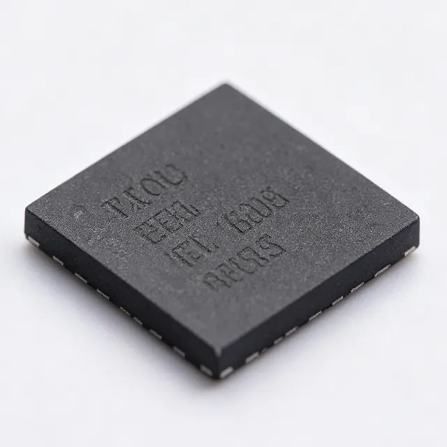
TIOL221RGER - Dual IO-Link PHY with LDO & SPI | TI
The Texas Instruments TIOL221 (TIOL221RGER) is a dual-channel IO-Link device physical layer (PHY) transceiver with an integrated LDO and SPI interface, supplied in a 24-pin VQFN (4x4 mm) package. It serves as the complete physical layer between an IO-Link master and a remote sensor or actuator node over the three-wire IO-Link interface (L+, L-, CQ). An IO-Link PHY (physical layer transceiver) is a specialized industrial communication interface IC that handles line driving, wake-up detection, and protection for point-to-point digital communication networks. Within the system hierarchy, it sits below the microcontroller (logic layer) and above the physical cabling, forming part of the broader industrial networking and sensor interface semiconductor category. Key features include dual CQ channels with integrated low-power output drivers featuring active reverse polarity protection, wake-up pulse generation and detection (sinking or sourcing >= 500 mA for a typical 80 us duration per IO-Link specification), and wake-up reporting to the local microcontroller by asserting the WU pin low. Internal protection covers undervoltage, overcurrent, and overtemperature conditions, with fault reporting to the host. The integrated LDO reduces external BOM count, and the SPI interface allows flexible configuration and diagnostics. The device can also be configured to generate wake-up pulses and be used in IO-Link master applications, and it integrates an auxiliary DI (digital input) channel. Typical applications include IO-Link sensor hubs, industrial proximity sensors, actuator nodes, and compact IO-Link master ports. Design tip: ensure the CQ driver thermal budget accounts for wake-up pulse current, and use the fault reporting pins for system-level diagnostics.