Pengurusan Kuasa
Subkategori
Produk (2,800+)

IXDN609YI - 9A Low-Side MOSFET/IGBT Gate Driver TO-263-5 | IXYS
The IXYS (Littelfuse) IXDN609YI is a 9-Ampere low-side, ultra-fast MOSFET/IGBT gate driver in a TO-263-5 (D2PAK) surface-mount package with 5 leads + tab. It delivers 9 A peak source/sink drive current, supports supply voltages from 4.5 V to 35 V, and exhibits propagation delays around 60 ns with rise/fall times below 25 ns. The part is logic-input CMOS-compatible, non-inverting, and the logic input withstands negative swings down to -5 V, making it robust against ground bounce and ringing on long gate-drive traces. Background: a gate driver is a power-management semiconductor that sits between a low-power control IC (MCU, FPGA, or analog controller) and the gate of a high-power switching device (MOSFET, IGBT, GaN, or SiC FET). Its role is to translate a logic-level PWM signal into a high-current, fast-rise/fall drive waveform that can charge and discharge the gate charge (Qg) of the switching transistor in nanoseconds. Within the broader hierarchy, gate drivers fall under power management ICs > MOSFET/IGBT drivers > low-side drivers; low-side means the driver switches the transistor's source to ground rather than floating the high-side rail, so it requires fewer components and is the most economical topology for buck converters, synchronous rectifiers, and motor half-bridge low-side switches. Key features include matched rise/fall times for low EMI, latchup-immune CMOS input stage, proprietary circuitry that eliminates cross-conduction, and an extended operating temperature range up to +125 °C. The TO-263-5 (D2PAK) tab provides a low thermal-resistance path for dissipating the gate-drive losses at high switching frequencies. According to the IXYS datasheet, output current ratings from 2 A to 30 A are available in this driver family for switching the largest MOSFETs and IGBTs at frequencies up to 10 MHz. Typical applications include high-frequency DC-DC converters, motor-drive low-side switches, Class-D audio amplifiers, power-conversion switching stages, and synchronous-rectifier drivers. The wide 4.5 V to 35 V supply range also makes it directly compatible with both 5 V and 12 V logic rails. When designing with this device, ensure the gate-drive loop is minimized: keep the driver-to-gate trace short and wide, place a small gate resistor (1-10 Ω) close to the gate to dampen ringing, and provide a local bypass capacitor (≥1 µF X7R) directly at the VCC pin to supply the 9 A peak transients. This page synthesizes distributor pricing, drop-in same-package alternatives (TO-263-5 D2PAK footprint), and engineering design notes drawn from the manufacturer datasheet and reference designs.

KA7500B - SMPS PWM Controller DIP-16 | onsemi
The onsemi KA7500B is a voltage-mode PWM controller IC designed for switch-mode power supplies (SMPS) and DC-DC converters, offered in a 16-pin PDIP (DIP-16) through-hole package with an absolute maximum supply voltage of 42 V and programmable switching frequency up to 300 kHz. It integrates a 5 V trimmed reference, on-chip oscillator, dead-time control, push-pull/single-ended output mode selection, and 200 mA sink/source output drivers for direct MOSFET drive in many topologies. The KA7500B is functionally equivalent to the industry-standard TL494 PWM controller family and is widely used as a drop-in replacement in legacy ATX, DC-DC, and inverter designs. A PWM controller (Pulse-Width Modulation controller) is a key building block in the power management IC hierarchy: PWM controller -> SMPS controller -> DC-DC controller -> power management IC. It regulates an output voltage by varying the duty cycle of a switching element (MOSFET or BJT) at a fixed frequency, enabling high-efficiency power conversion versus linear regulation. The KA7500B is a voltage-mode controller, meaning it regulates by comparing an error-amplifier output against an internal sawtooth ramp - a topology prized for its simplicity, predictable loop compensation, and noise immunity. Key features include a stable on-chip 5 V reference trimmed to 5%, uncommitted output transistors rated for 200 mA sink or source current, variable dead-time control on pin 4 for cross-conduction prevention, output mode selection for either push-pull (half-bridge/full-bridge) or single-ended operation, and a complete PWM power-control circuitry including error amplifiers, oscillator, and reference. The on-chip oscillator can be synchronized to an external master clock for multi-rail power systems, and the uncommitted outputs enable flexible topology choice. Operating temperature range is typically 0C to 70C (commercial grade). Typical applications include ATX/PC power supplies, DC-DC buck/boost/half-bridge converters, solar inverters, and uninterruptible power supplies. It also appears in welding equipment, induction heaters, and motor drives where TL494-class TL494 replacements are needed. The Ka7500B's DIP-16 through-hole package simplifies prototyping, repair, and retrofit work on legacy PCBs that were designed around the TL494 pinout. When designing with this device, ensure the oscillator timing resistor RT and capacitor CT are selected to set the switching frequency below 300 kHz with adequate margin. Add proper bypass capacitance on VCC and VREF, and use the dead-time control pin to set the minimum off-time to prevent simultaneous conduction of the push-pull output transistors. This page synthesizes distributor pricing, drop-in TL494-family alternatives, and practical design notes not consolidated in any single manufacturer datasheet.

KTA1136EUAE-TR - 13W 802.3af PoE PD Controller | Kinetic
The Kinetic Technologies KTA1136EUAE-TR is an IEEE 802.3af Power over Ethernet (PoE) Powered Device (PD) controller with an integrated DC-DC controller and 13W power FET, housed in a 16-pin TQFN (4x4 mm) package. A PoE PD controller is a power-management IC that sits at the powered end of an Ethernet link and performs the handshake required by the IEEE 802.3 standard: it presents the correct detection signature to the Power Sourcing Equipment (PSE), communicates its power class, and disconnects the load until valid power is negotiated. Within the power-management IC hierarchy, a PoE PD controller occupies the system-power layer between the RJ45/magnetics input stage and the downstream DC-DC conversion stage. The KTA1136 integrates input surge protection, a PD controller with a 100V-rated hot-swap FET, a DC-DC converter controller, and a robust 150V-rated switching power MOSFET in a single chip. This high level of integration eliminates the external pass transistor, hot-swap circuitry, and switching controller typically required in a discrete PoE PD design, reducing bill-of-material count and board area. It implements all physical-layer PD functionality required by IEEE 802.3af-2003, including PD detection, classification, under-voltage lockout (UVLO), and hot-swap FET control, and is also listed by distributors as supporting 802.3at (PoE+) and 802.3bt listings. Typical applications include Voice over IP (VoIP) phones, wireless access points, IP security cameras, and other 13W-class PoE powered devices. The integrated 13W power stage makes it well matched to single-class PD endpoints that draw power directly from the 48V Ethernet rail. When designing with this part, verify the external DC-DC power stage component ratings against the integrated 150V MOSFET and follow the manufacturer datasheet layout guidance for the hot-swap and switching nodes. This page synthesizes distributor data, cross-reference findings, and engineering design context not found in a single datasheet, including verified source links and lifecycle information.

KTA1137AEUAB-TR - 30W 802.3at PoE PD Controller | Kinetic
The Kinetic Technologies KTA1137AEUAB-TR is a single-chip IEEE 802.3at (PoE+) and 802.3af (PoE) Powered Device (PD) controller with an integrated DC-DC controller, supporting up to 30W input power in a 20-TQFN (5x5 mm) package. A Power over Ethernet Powered Device controller is the interface IC that performs PD detection, classification, and inrush current limiting when a device such as an IP camera, wireless access point, or VoIP phone draws power from Ethernet cabling. It sits within the power management IC hierarchy, combining the PoE handshaking front end and a switching power supply controller in a single CMOS die, which removes the need for a separate PWM controller in many designs. Key features include compliance to both IEEE 802.3af (13W) and IEEE 802.3at (30W) power classes, an integrated DC-DC controller optimized for isolated and non-isolated converter topologies, and single-chip CMOS integration that reduces bill-of-materials count. According to Kinetic Technologies product documentation, the KTA1137A family is a highly integrated solution for PoE Powered Devices requiring input power of up to 30 watts. On the technical side, the device supports flyback converter topologies; the manufacturer evaluation board (KTA1137AEUAB-MMEV02) demonstrates a 12V, 25W flyback converter for PD applications, confirming real-world performance near the full 30W capability. The integrated controller architecture simplifies transformer-based isolated designs as well as non-isolated buck-derived converters. Typical applications include IP security cameras, 802.11ac/ax wireless access points, VoIP telephones, network switches with PD ports, and building automation endpoints that must be powered entirely over standard Ethernet cabling. A key design consideration is that the KTA1137A is pin compatible with the discontinued AS1138, so engineers migrating legacy AS1138-based PD designs can substitute with minimal PCB rework. Verify transformer specifications against the target output power class. This page synthesizes distributor availability data, the AS1138 pin-compatibility cross-reference, and practical design context not found in the manufacturer datasheet alone.

KTS1681AEUZ-TR - 4A OVP Load Switch with +100V Surge | Kinetic
The Kinetic Technologies KTS1681AEUZ-TR is a 4 A overvoltage-protected load switch with integrated 28 mOhm (typical) MOSFET and +100 V surge protection, housed in a 12-ball WLCSP package (1.7 x 1.21 mm). It is engineered to actively shield downstream low-voltage systems from voltage supply faults up to +28 VDC and transient surges as high as +100 V at the input. A load switch, in this category, is a power-distribution switch that sits between an upstream supply rail and downstream electronics, controlling power-up, power-down, and fault isolation. The KTS1681A family specifically addresses overvoltage (OVP) events - it occupies the niche between discrete TVS diodes plus MOSFETs and full hot-swap controllers, integrating an internal clamp, OVP comparator, and power MOSFET into a single IC. It belongs to the broader class of power-management ICs (PMICs) and is functionally adjacent to surge suppression and eFuse devices. Key differentiating features include an adjustable overvoltage trip threshold, a sense output for load current monitoring, an internal clamp that absorbs surges to +100 V without external TVS components, ultra-low 28 mOhm on-resistance to minimise conduction losses, and a 12-WLCSP form factor that is the smallest footprint in its class. The internal clamp eliminates the need for an external TVS diode in most 28 V hot-plug and automotive use cases. The device architecture combines a back-to-back MOSFET configuration for true bidirectional blocking, an internal clamp for surge absorption, and an OVP comparator that triggers switch turn-off when VIN exceeds the programmed threshold. The sense output provides an analog current-mirror signal proportional to load current, simplifying accurate load-current telemetry without a series sense resistor. Typical applications include USB Type-C VBUS protection, smartphone and tablet charging ports, hot-plug circuits on multi-rail systems, and any point-of-load where 5 V/9 V/12 V/20 V rails may be exposed to faulty or miswired supplies. The WLCSP-12 footprint is preferred over larger QFN packages when board area is at a premium. When designing in this part, choose the OVP threshold carefully so that transient overshoot from normal hot-plug events does not falsely trigger the protection. Adequate input decoupling is required to keep the internal clamp from sustained clamping operation, which can raise junction temperature beyond the device rating. This page synthesises distributor pricing, WLCSP-12 pin configuration, and matching same-family load switches that share the same footprint - information not consolidated on any single distributor page.

L2720D - Voltage Regulator | Technical Data and Alternatives
The L2720D is an electronic component identified by the manufacturer part number L2720D and is presented in the Power Management > Voltage Regulators category for technical research purposes. No manufacturer datasheet, official product page, distributor listing, package diagram, lifecycle statement, or verified electrical specification was returned by the supplied real-time search on October 29, 2026. Consequently, the available confirmed identity for this record consists of the MPN, its regulator-category placement, and the search timestamp rather than manufacturer-specific performance data. A voltage regulator is a power-management semiconductor that maintains a controlled supply voltage as its input voltage or load changes. Depending on its architecture, a device in this category may use linear regulation, switching conversion, or another feedback method. The L2720D requires verification against its manufacturer datasheet before its topology, adjustable or fixed output behavior, current rating, dropout voltage, input-voltage limits, thermal limits, and package details can be used in a design. The verified input for L2720D did not include electrical characteristics, absolute maximum ratings, tolerance, quiescent current, line regulation, load regulation, protection features, environmental ratings, or compliance declarations. These values are therefore not stated as specifications in this page. An engineer should not infer them from the part number, a distributor search result, or a visually similar regulator. The missing fields require direct confirmation from the responsible manufacturer or an authoritative internal component record. The MPN suffix cannot safely be interpreted without the associated package data. It may identify a temperature grade, package option, lead-finish configuration, or ordering code, but no confirmed package mapping was supplied. Pin compatibility, PCB footprint, exposed-tab requirements, and soldering details consequently remain unverified. This uncertainty is especially important because regulators with similar output-current and voltage ratings can use incompatible lead assignments or thermal arrangements. Potential uses must remain conditional until the electrical limits are confirmed. A designer may be evaluating an L2720D for industrial control, instrumentation, communications equipment, consumer electronics, or another regulated supply, but suitability depends on the actual input range, output voltage, available dissipation, ambient temperature, and required accuracy. The decision should use verified worst-case values rather than nominal or assumed ratings. Before procurement or schematic capture, obtain the official L2720D datasheet, confirm the manufacturer and lifecycle status, verify the exact ordering suffix and package, and compare the pinout against the assembled PCB. If the original part is unavailable, an equivalent must have the same footprint and pin functions as well as compatible voltage, current, thermal, and timing characteristics. Tape-and-reel codes alone are not electrical substitutes. This page distinguishes confirmed metadata from unverified technical attributes and avoids presenting inferred specifications as facts. Its unique value is the explicit audit trail: it identifies every missing datasheet and cross-reference item, preserves the failed-search context dated October 29, 2026, and supplies selection and validation guidance without fabricating prices, pin assignments, package names, or replacement MPNs.

L298N - Dual Full-Bridge Driver, 46V/2A | STMicroelectronics
The STMicroelectronics L298N is a high-voltage, high-current dual full-bridge driver integrated in a monolithic IC and housed in a 15-lead Multiwatt vertical package with an exposed metal tab for through-hole heatsinking. Each bridge delivers up to 2 A continuous and the device accepts standard TTL logic levels at the inputs, making it directly compatible with 5 V microcontrollers, Arduino boards, and 3.3 V logic when level-shifted. The two bridges can be operated in parallel for higher current or independently to drive two DC motors, a bipolar stepper, or any combination of inductive loads such as relays and solenoids. A dual H-bridge motor driver is a power-stage topology that uses four switches arranged so the polarity of the DC voltage applied to a motor can be reversed electronically, enabling forward, reverse, and dynamic braking from a single supply rail. H-bridges belong to the broader family of DC motor drivers, which sit under the power-management hierarchy of integrated circuits and are most often used to bridge low-power digital logic with high-power electromechanical actuators. Key features include a 46 V maximum supply rating (Vs), 2 A continuous per bridge (4 A peak), TTL-compatible enable and input pins, internal clamp diodes for inductive kickback protection, and a logic supply range of 4.5 V to 7 V. Two independent enable inputs (ENA, ENB) allow the user to disable each bridge for PWM speed control or fault response. Thermal shutdown is not internally provided and must be managed by external sensing or by limiting average current. The L298 uses bipolar Darlington output stages, which produces a high voltage drop (typically ~2 V at 1 A) that is dissipated as heat. This is the trade-off for the part's ruggedness and low cost. Modern MOSFET-based drivers such as the TB6612FNG achieve much higher efficiency, but the L298 remains the de-facto choice for hobby robotics, CNC prototyping, and educational platforms because it is inexpensive, easy to wire, and proven across decades of designs. Typical applications include DC motor speed and direction control in two-wheel-drive robots, bipolar stepper motor drives for 3D printers and CNC routers, solenoid and relay drivers in industrial automation, and pump/valve control in fluid handling. The Multiwatt-15 package is designed for a TO-220-style clip-on heatsink and accepts a 5 mm screw mount, which is the recommended way to operate the part above 1 A per bridge continuously. When designing with this part, always add flyback diodes if driving non-resistive loads and derate to roughly 1 A per bridge when no heatsink is attached. The 5 V jumper on the popular breakout modules enables the on-board 78M05 logic regulator; remove it when an external 5 V rail is already present to avoid back-powering the Arduino.

L4931ABD50 - 5V 250mA LDO Regulator with Inhibit | STMicroelectronics
The STMicroelectronics L4931ABD50 is a 5 V very low-dropout (LDO) linear regulator delivering up to 250 mA of output current in an 8-pin SOIC package. The ABD50 variant offers a fixed 5.0 V output, a maximum dropout of 0.4 V at full load, and a quiescent current that stays low even in standby. The SO-8 version integrates a TTL-compatible inhibit pin for shutdown sequencing, making it suitable for the position of a clean, low-noise rail in mixed-signal systems. An LDO (Low-Dropout) linear regulator is a type of voltage regulator that maintains a stable output voltage even when the input-to-output differential is small, typically a few hundred millivolts. Within the broader power-management hierarchy, LDOs belong to the linear regulator family, which itself sits under voltage regulators and the overall power management IC category. LDOs are favored over switching regulators in noise-sensitive applications because they introduce no EMI from switching action, and they typically provide high PSRR and low output noise. Key features of the L4931ABD50 include a very low dropout of 0.4 V at 250 mA, low quiescent current in both operating and inhibit states, internal current limit with thermal shutdown protection, and a TTL-compatible inhibit (shutdown) pin on the SO-8 package. The fixed 5 V output eliminates external resistor dividers and simplifies PCB layout, while the SO-8 footprint provides compact board integration with adequate copper area for sustained 250 mA delivery. The L4931 series uses a PNP pass transistor architecture with a precision bandgap reference, achieving tight line and load regulation across the operating range. The internal inhibit logic is TTL-compatible, allowing direct interface with microcontrollers or logic gates without level shifting. Combined with very low quiescent current, this makes the part particularly efficient in battery-powered and always-on subsystems where standby drain matters. Typical applications include battery-powered portable devices, microcontroller and DSP supply rails, post-regulation after a switching converter to clean ripple, automotive ECUs (the L4931 is AEC-Q100 qualified for automotive markets), and any system requiring a 5 V rail with low dropout and shutdown control. When designing with this device, ensure adequate input and output capacitance (typically 2.2 µF minimum on each) for regulator stability, and respect the 0.4 V dropout budget under all load transients. The inhibit pin should be tied high (or left open, since the SO-8 version enables by default) when shutdown is not required. This page synthesizes distributor pricing, drop-in alternatives, and practical design notes not found in the manufacturer datasheet alone.

L4984DTR - Current-Mode CCM PFC Controller | STMicroelectronics
The STMicroelectronics L4984DTR is a current-mode power-factor-correction controller operating in continuous-conduction mode with line-modulated fixed-off-time control. It accepts a 10.3 V to 22.5 V supply, features 1.1 V lockout and a 65°C startup threshold, and is packaged in a 10-lead SSOP. The device is designed for mains-powered switching systems requiring active power-factor correction. A power-factor-correction controller is a specialized power-management IC that shapes input current drawn from an AC line. By commanding a switching converter at the proper timing, it reduces reactive current and improves the line power factor. The L4984D belongs to the PFC-controller hierarchy and supports boost-type front ends commonly placed ahead of downstream DC-DC converters in industrial, commercial, and consumer power supplies. The supplied L4984D information identifies continuous-conduction operation, current-mode control, LM-FOT modulation, a 10.3 V to 22.5 V supply range, 1.1 V lockout, and approximately 5 mA operating current from distributor technical summaries. The 10-SSOP package supports compact surface-mount layouts. These values should be checked against the complete manufacturer datasheet before production release because the verified data does not include every timing, threshold, gate-drive, and protection parameter. In a typical boost PFC stage, the controller senses inductor or input current and regulates the switching command so the input waveform is shaped toward unity power factor. LM-FOT control adapts the off-time to line conditions, while continuous-conduction mode favors lower current ripple than discontinuous operation. The external power stage, current-sense network, compensation components, and protection thresholds remain design-specific. L4984DTR is suited to offline AC-DC front ends, server and telecom power systems, industrial power supplies, and consumer adapter designs when an active PFC stage is required. Designers must validate startup behavior, loop stability, inductor sizing, MOSFET selection, current-sense limits, and safety isolation under their operating line range. The principal design consideration is that controller selection is only one part of PFC qualification. Check the exact STMicroelectronics datasheet and reference design for recommended gate-drive, compensation, sensing, and protection values. Confirm whether the 10-SSOP footprint, pin functions, voltage limits, and switching timing match the target PCB before committing to a drop-in replacement. This page consolidates the verified L4984DTR product-page and distributor information, explicitly separates known values from unavailable data, and provides replacement guidance without presenting unverified substitutes as drop-in equivalents.
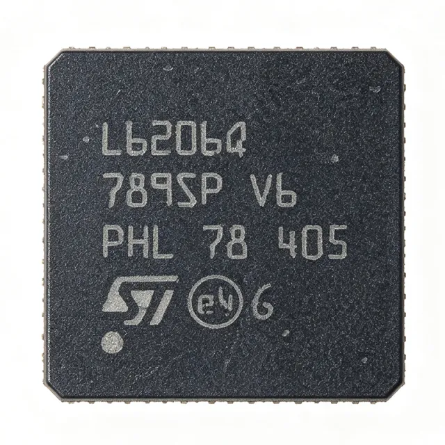
L6206Q - Dual DMOS Full-Bridge Driver 8A | STMicroelectronics
The STMicroelectronics L6206Q is a dual DMOS full-bridge motor driver capable of delivering up to 2.8A per channel (8A peak total) in a 48-pin QFN (QFN48) package. It operates from a supply voltage range of 8V to 52V, making it suitable for a wide variety of industrial and automotive motor control applications. The device integrates two independent H-bridges with a total output current of 5.6A continuous (2.8A per bridge), and includes thermal shutdown and undervoltage lockout protection. A DMOS full-bridge driver is a type of power integrated circuit that uses four N-channel DMOS transistors arranged in an H-bridge configuration to control the direction and speed of a DC motor or the phase currents of a stepper motor. It belongs to the broader category of motor drivers, which are power management ICs that translate low-power control signals into high-current, high-voltage outputs. The L6206Q sits in the hierarchy: DMOS full-bridge driver -> motor driver -> power management IC -> semiconductor. Key features include a low RDS(on) of 0.3 ohm per switch, which minimizes power dissipation and improves efficiency, and a fast switching frequency of up to 100 kHz, enabling precise PWM control. The device also features a non-dissipative overcurrent protection (OCP) that limits the output current to a safe level, and a diagnostic output that indicates fault conditions. The QFN48 package provides a compact footprint with an exposed thermal pad for enhanced heat dissipation. The L6206Q uses a mixed-signal BCD (Bipolar-CMOS-DMOS) process technology, integrating the DMOS power stage with CMOS control logic and bipolar protection circuits. This architecture allows for high current handling with low quiescent current and robust protection features. The device supports both parallel and bridge configurations, enabling flexible motor drive topologies. Typical applications include bipolar stepper motor drivers, DC motor drivers for robotics and automation, and brushless DC motor pre-drivers. The wide supply voltage range and high current capability make it ideal for industrial automation, CNC machines, and automotive actuators. In a stepper motor application, the L6206Q can drive two-phase motors with up to 2.8A per phase, providing smooth microstepping control. When designing with this device, ensure adequate PCB copper area for the thermal pad to dissipate heat, especially at high output currents. The VREF pin allows current sensing and regulation, which is essential for torque control in stepper applications. The EN pins provide independent enable control for each bridge, enabling power-saving modes. This page synthesizes distributor pricing, drop-in alternatives, and practical design notes not found in the ST datasheet, providing a comprehensive resource for engineers selecting a dual full-bridge driver.

L6207PD - DMOS Dual Full Bridge Motor Driver, 52V/2.8A | STMicroelectronics
The STMicroelectronics L6207PD is a DMOS dual full-bridge motor driver realized in MultiPower BCD technology, delivering up to 2.8 A continuous per bridge from an 8 V to 52 V supply in a PowerSO-36 slug-up package with exposed thermal pad. What is a DMOS dual full-bridge motor driver? It is an integrated power stage that contains four power DMOS transistors arranged as two complete H-bridges, plus on-chip logic and current-control circuitry, used to bidirectionally drive DC motors, stepper motors, or solenoids from a single supply rail. Within the broader product hierarchy, the L6207PD sits in the motor driver IC family, which belongs to power management semiconductors, a category that also includes voltage regulators, gate drivers, and motor controllers. Key features include a wide 8 V to 52 V operating supply range, 2.8 A continuous output current per bridge (with 5.6 A peak capability in PWM mode), on-chip dual independent constant-off-time PWM current controllers with programmable chopping, integrated non-dissipative overcurrent protection, thermal shutdown, and cross-conduction prevention logic. The BCD process combines isolated DMOS output transistors with CMOS and bipolar control circuitry on a single die, eliminating external gate-drive components and reducing PCB area. The DMOS output stage achieves low on-resistance RDS(on) of approximately 0.3 ohm per switch, which directly improves efficiency and reduces conduction losses compared with bipolar Darlingtons predecessors. The integrated dual PWM current controllers enable precise torque regulation in stepper motors by chopping the phase current at a user-defined threshold set via an external sense resistor and RC network, eliminating the need for an external microcontroller PWM loop. Typical applications include bipolar stepper motor drives, DC motor bidirectional control in industrial automation, positioning stages, and solenoid/valve drivers. The high 52 V supply tolerance also makes it suited for 24 V and 48 V industrial bus systems. The PowerSO-36 slug-up exposed pad package provides low thermal resistance, enabling continuous high-current operation with appropriate PCB copper area. When designing with this part, the user must provide sense resistors on the SENSE pins, set the OFF time through the RC pin, and observe the absolute maximum supply of 60 V. Heat sinking via PCB copper or an external heatsink on the slug-up tab is essential at currents above 1.5 A per bridge to maintain junction temperature within the 150 C limit.

L6470H - dSPIN Stepper Motor Driver | STMicroelectronics | HTSSOP-28
The STMicroelectronics L6470H is a fully integrated microstepping motor driver with an embedded dSPIN™ motion engine, delivering up to 3 A peak output current per phase in a 28-pin HTSSOP (PowerSO-28) package. It operates from a supply voltage range of 8 V to 45 V and features programmable microstepping up to 1/128 step, making it suitable for high-resolution motion control applications. Data verified as of 2026-08-05. A stepper motor driver is a power management IC that translates digital step and direction commands into the precise current sequences needed to rotate a bipolar stepper motor. The L6470H belongs to the motor driver category, which sits within the broader power management IC hierarchy: motor driver -> power management IC -> semiconductor. Its integrated motion engine offloads complex acceleration and deceleration profiles from the host microcontroller, enabling smoother motion and reduced processor load. Key features include a programmable motor current from 0 mA to 3 A RMS, SPI interface for configuration and control, and a wide range of protection features such as overcurrent, overtemperature, and undervoltage lockout. The device also integrates a 1/128 microstepping capability, which significantly reduces motor noise and vibration compared to full-step operation. The HTSSOP-28 package with exposed pad provides excellent thermal performance, with a thermal resistance of 25 °C/W, enabling operation at high currents without external heatsinking in many applications. The L6470H uses a proprietary dSPIN™ architecture that combines a power stage, current sensing, and a motion profile generator on a single die. This integration reduces external component count and simplifies PCB layout. The SPI interface allows real-time adjustment of motor parameters, such as acceleration, deceleration, and target speed, enabling adaptive motion control in dynamic systems. The device also supports daisy-chaining of multiple drivers on a single SPI bus, simplifying multi-axis systems. Typical applications include 3D printers, CNC machines, robotics, and automated textile machinery. In a 3D printer, the L6470H's high microstepping resolution and quiet operation are critical for achieving precise layer deposition and reducing print artifacts. In robotics, the integrated motion engine allows smooth, controlled movement of joints and actuators, improving overall system performance. When designing with the L6470H, ensure adequate supply decoupling with a 100 nF ceramic capacitor close to the VSA and VSB pins, and a bulk capacitor (≥10 µF) on the supply rail. The exposed pad must be soldered to a large copper area for thermal management. The SPI lines should be kept short and shielded to avoid noise coupling into the motor current sense circuitry. This page synthesizes distributor pricing, drop-in alternatives, and practical design notes not found in the ST datasheet, providing engineers with a comprehensive resource for evaluating the L6470H in their motion control designs.

L6470HTR - dSPIN Stepper Motor Driver | STMicroelectronics
The L6470HTR is a fully integrated microstepping motor driver from STMicroelectronics, part of the dSPIN family. It combines a complete motor control system on a single chip, including a power stage with dual full-bridge drivers, a digital control core, and a serial interface. The device is designed to drive bipolar stepper motors with up to 3 A peak current per phase, operating from a supply voltage range of 8 V to 45 V. It is available in a compact HTSSOP28 package, making it suitable for space-constrained applications. A stepper motor driver is a power management IC that translates digital step and direction commands into the precise current sequences needed to rotate a stepper motor. The L6470HTR integrates the control logic, gate drivers, and power MOSFETs, eliminating the need for external components and simplifying PCB design. It belongs to the hierarchy: stepper motor driver -> motor driver -> power management IC -> semiconductor. This integration reduces system cost and board space while improving reliability. Key features of the L6470HTR include programmable microstepping up to 1/128 step, which provides smooth motion and high positioning accuracy. It offers a wide range of protection features, including overcurrent, overtemperature, and undervoltage lockout. The device also includes a SPI interface for configuration and control, allowing real-time adjustment of motor parameters. The integrated current sensing eliminates the need for external sense resistors, further reducing component count. The L6470HTR uses a proprietary control algorithm that automatically adjusts the current decay mode to optimize performance across different motor types and load conditions. This adaptive decay control minimizes audible noise and power dissipation. The device also features a programmable slew rate to reduce electromagnetic interference (EMI) in sensitive applications. The digital core operates at up to 16 MHz SPI clock, enabling fast communication with microcontrollers. Typical applications include 3D printers, CNC machines, robotics, office automation, and industrial automation. In 3D printers, the L6470HTR provides precise filament positioning with microstepping, resulting in high-quality prints. In CNC machines, it drives stepper motors for axis movement with high torque and accuracy. The device's wide voltage range and current capability make it versatile for various motor sizes. When designing with the L6470HTR, ensure proper thermal management by providing adequate copper area on the PCB for heat dissipation. The HTSSOP28 package has an exposed pad that must be soldered to a thermal relief. Additionally, place decoupling capacitors close to the power supply pins to minimize voltage transients. The SPI interface allows configuration of motor parameters, but careful attention to the register settings is required to avoid unintended behavior.
L6480H - 10A Dual Full-Bridge Stepper Motor Driver | STMicroelectronics
The STMicroelectronics L6480H is a fully integrated dual full-bridge stepper motor driver capable of delivering up to 10A peak output current per bridge, designed for high-performance motion control applications. It operates from a supply voltage range of 8V to 85V and integrates a complete digital control core with SPI interface, making it a versatile solution for industrial automation, robotics, and CNC machinery. The device is housed in a 28-pin HTSSOP (H) package with an exposed thermal pad, enabling efficient heat dissipation in compact designs. Data verified as of 2026-08-05. A stepper motor driver is a power management IC that translates digital step and direction commands into precise current-controlled pulses for driving bipolar stepper motors. It sits within the hierarchy: stepper motor driver -> motor driver -> power management IC -> semiconductor. The L6480H integrates both the power stage and the control logic, eliminating the need for external MOSFETs and simplifying PCB design. This integration reduces component count and improves reliability, making it a key building block in modern motion control systems. Key features of the L6480H include a programmable output current up to 10A peak, microstepping up to 1/128 step, and a wide supply voltage range of 8V to 85V. It also features overcurrent, overtemperature, and undervoltage protection, ensuring robust operation in harsh industrial environments. The SPI interface allows real-time configuration and monitoring, while the dedicated STEP and DIR pins enable simple interfacing with microcontrollers or motion controllers. The L6480H utilizes a proprietary advanced current control algorithm that minimizes motor noise and vibration, improving positioning accuracy. The device supports both full-step and microstepping modes, with the ability to adjust the decay mode for optimal performance across different motor types. The integrated sense resistors eliminate the need for external current sensing, further reducing BOM cost and board space. Typical applications include CNC machines, 3D printers, textile machinery, and automated assembly equipment. The L6480H's high current capability and wide voltage range make it suitable for driving large NEMA 34 and NEMA 42 stepper motors, which are common in industrial automation. Its SPI interface also enables advanced features like stall detection and position tracking, enhancing system intelligence. When designing with the L6480H, ensure adequate PCB copper area for thermal dissipation, as the device can dissipate significant power at high currents. The exposed pad must be soldered to a thermal via array connected to a ground plane. Additionally, place decoupling capacitors close to the VM and VCC pins to minimize voltage transients. This page synthesizes distributor pricing, drop-in alternatives, and practical design notes not found in the STMicroelectronics datasheet, providing engineers with a comprehensive resource for selecting and implementing the L6480H in their designs.
L6561D013TR - Transition-Mode PFC Controller | STMicroelectronics
The STMicroelectronics L6561D013TR is a current-mode power-factor-correction controller operating in transition mode, with a nominal 13 V output and an 8-pin SOIC package. It is designed for boost PFC stages in offline power supplies, where it controls input current to improve power factor and reduce input-current distortion. According to the manufacturer product page, L6561 is compatible with the standard L6560 architecture and supports wide input-voltage applications from 85 V to 265 V with low total harmonic distortion. A PFC controller is a power-management IC that shapes the current drawn from an AC input so that the input current is more closely in phase with the input voltage. In boost PFC, the controller drives a switching converter between the rectified mains input and a higher DC bus. The transition-mode control approach improves input-current shaping while supporting high power-factor power supplies used in industrial equipment, chargers, servers, and power-factor-correction front ends. Key features reported for the L6561 family include an adjustable output-overvoltage protection function, a 50 uA typical startup current, a 4 mA typical operating supply current, an internal startup timer, an on-chip current-sense filter, an internal disable function, and a 1% internal reference at 25 C. The transition-mode PFC function is intended for wide-input applications where reduced harmonic distortion and controlled boost operation are important. The L6561D013TR is supplied in an 8-pin SOIC package. Its suffix identifies the STMicroelectronics ordering configuration, while the D013TR part is associated with a 13 V nominal variant in the distributor data. Exact pin names, voltage limits, switching thresholds, timing values, and absolute maximum ratings should be confirmed from the official STMicroelectronics datasheet before final circuit design, because those parameters are not included in the supplied verification snippets. Typical applications include AC-DC power-factor-correction stages for industrial and consumer power supplies, server or telecom power systems with active PFC, battery-charging front ends, and offline converters requiring harmonic-current reduction. The controller is normally placed around a boost switch, inductor, rectified input bridge, sensing network, and protection circuitry. Component values must be calculated from the target bus voltage, output power, input range, switching frequency, inductor ripple, and current-sense threshold. A key design consideration is the interaction between the controller, boost inductor, MOSFET, rectifier bridge, and current-sense network. Keep the current-sense path short and shielded from high-dV/dt switching nodes, select the MOSFET and rectifier for the intended voltage and current stresses, and validate startup, overvoltage, line transients, and thermal behavior over the complete input range. This page combines verified distributor data, manufacturer information, replacement research, and practical design guidance.
L6562D Transition-Mode PFC Controller | STMicroelectronics
The STMicroelectronics L6562D is a current-mode power-factor-correction controller operating in transition mode, with a 1 MHz switching-related specification, a 10.3 V to 22 V supply range, and an SOIC-8 package. It is designed for boost PFC preregulators in AC power supplies and electronic ballasts. According to the manufacturer’s product description, the L6562 is pin-to-pin compatible with its L6561 predecessor while providing improved performance. A power-factor-correction controller is a specialized power-management IC that shapes the input current drawn from an AC rectifier so that it is closer to sinusoidal and has a near-unity power factor. In a boost PFC stage, the controller regulates the DC output bus while monitoring input current and voltage. This reduces reactive current, lowers input-current distortion, and helps the power stage comply with power-quality requirements. The L6562D features a proprietary multiplier design for minimum AC-input-current total harmonic distortion, precise adjustable output-overvoltage protection, ultra-low start-up current of 70 µA, and low quiescent current of approximately 4 mA. The verified distributor data identifies the device as a discontinuous/transition-mode PFC controller rated for operation from a 10.3 V to 22 V supply, with 10.3 V lockout and approximately 3.5 mA supply current in another distributor description. The exact maximum output-voltage and compensation details should be confirmed against the manufacturer datasheet before production release. Typical applications include server and telecom power supplies, industrial AC-DC converters, LED-driver front ends, electronic ballasts, and other boost PFC preregulators. The controller’s current-mode architecture supports cycle-by-cycle current control, while transition-mode operation allows the switching frequency to vary with the rectified input voltage. Designers must still validate loop compensation, inductor sizing, MOSFET selection, startup behavior, fault thresholds, and safety isolation in the final reference design. The main design consideration is that controller substitution is not automatically safe even when the package is similar. A candidate must match the L6562D pin functions, control architecture, timing behavior, voltage thresholds, compensation method, and protection strategy. Use the manufacturer datasheet and the application circuit as the authority rather than relying on distributor category descriptions alone. This page consolidates verified distributor and manufacturer links, identifies the supported L6561 compatibility statement, and separates known engineering facts from missing specifications. Use it for initial component selection and sourcing, then complete a manufacturer-level design review for compliance and production use.

L6566BHTR - Multimode SMPS PWM Controller, 16-SO | STMicroelectronics
The STMicroelectronics L6566BHTR is a current-mode PWM controller for high-performance offline flyback converters operating from rectified 3-phase or single-phase universal mains, packaged in a 16-pin SO (16-SOIC, 0.154" / 3.90 mm width) and supplied on tape-and-reel. It combines a fixed-frequency (FF) mode and a quasi-resonant (QR) valley-skipping mode selectable via the user's load profile, switching at frequencies from 10 kHz up to 300 kHz. Key headline parameters are: 800 V on-board high-voltage start-up, 8 V to 23 V VCC supply range, and 3 mA quiescent current. According to the manufacturer datasheet, the controller integrates all the loops and protections required for offline SMPS designs, including a precise current-mode core with line-voltage feed-forward, programmable dead-time, and over-current / over-load / over-voltage latched disable. A primary-side SMPS controller (PWM controller) is the analog brain of an isolated switching power supply. It senses output voltage and primary current, generates the duty-cycle command for the external high-voltage MOSFET, and orchestrates soft-start, frequency modulation, and fault shutdown. Primary controllers sit hierarchically inside AC-DC converters -> offline switchers -> switch-mode power supply (SMPS) ICs -> power management semiconductors, and are commonly described using synonyms such as "current-mode PWM controller", "quasi-resonant controller", or "flyback controller". The L6566BH features multimode operation: at light load the IC enters valley-skipping quasi-resonant mode to minimise switching losses and EMI; at heavier load it transitions to fixed-frequency CCM/DCM. Advanced light-load management, 800 V high-voltage start-up, low quiescent current of 3 mA, and 750 mW power dissipation are core specifications. These translate into compact, efficient, and thermally-friendly adapters and open-frame supplies for both consumer and industrial white-goods markets. Architecturally, the L6566BH uses a peak-current-mode control loop with input-voltage feed-forward to deliver constant loop gain across the universal mains range (90 V to 264 V AC, or 3-phase rectified 380 V DC). Quasi-resonant valley switching keeps the MOSFET turn-on loss low and lowers EMI harmonics versus hard-switched PWM, while fixed-frequency operation guarantees predictable EMI signatures for worst-case load. The internal 800 V start-up cell eliminates the auxiliary winding bias resistor chain at start-up and survives input surges on the rectified mains bus. Typical applications include notebook and tablet adapters (45 W to 120 W), LCD-TV and monitor SMPS sub-modules, set-top box and white-goods offline supplies, and industrial auxiliary rails in 3-phase systems. The 8 V to 23 V VCC range also suits 12 V or 24 V distributed-bus front-ends. When using the L6566BH, allocate at least 1 cm² of copper around the SO-16 thermal pad footprint to keep junction rise below 70 °C, and use a 1 nF to 10 nF X7R timing capacitor on the timing pin to keep frequency drift under 5 % over the full operating temperature range.
L6566BTR - Multi-Mode PWM SMPS Controller, 300kHz, SO-16 | STMicroelectronics
The STMicroelectronics L6566BTR is a multi-mode current-mode PWM controller for high-performance offline flyback converters, packaged in a 16-pin SO (SO-16) tape-and-reel format. It combines a fixed-frequency and quasi-resonant topology switchable on the fly, on-board 700 V high-voltage start-up, and a 10 kHz to 300 kHz programmable switching range. The controller integrates adaptive UVLO, line feedforward for constant power vs. mains, and advanced light-load management that reduces quiescent current to about 3 mA. What is a multi-mode SMPS controller? It is a power-supply control IC that automatically transitions between operating modes - typically quasi-resonant (valley-switching) at high load and frequency-foldback or burst-mode at light load - to optimize efficiency across the entire load curve. The L6566B family belongs to ST's L65xx power-management portfolio, used as the primary-side controller in AC-DC switch-mode power supplies. The hierarchy is: PWM controller -> SMPS controller -> power management IC -> semiconductor. Key features include 8 V to 23 V supply range, 800 mA peak source/sink gate drive capability, programmable maximum duty cycle, overcurrent protection with fault counter, and transformer-saturation detection. The integrated high-voltage startup eliminates the external startup resistor network, reducing BOM count and standby loss. These specifications make the L6566BTR suited for compliance-driven adapters, set-top boxes, and white-goods SMPS designs targeting ENERGY STAR and EuP Tier-2 standby targets. The 'UVLO' (Undervoltage Lockout) and 'PWM' (Pulse Width Modulation) abbreviations are industry-standard. Architecturally, the L6566BTR uses a current-mode control loop with a leading-edge blanking, plus a valley-detection block that identifies the drain-voltage valleys for quasi-resonant switching. The 700 V startup MOSFET is rated for direct connection to the rectified mains, and the controller auto-restarts on fault events with user-programmable retry timing. The 16-pin SO package is JEDEC-standard (SO-16 narrow body, 150 mil) for surface-mount assembly, with RoHS-compliant lead-free finish and MSL Level 1 moisture rating. Typical applications include notebook adapters, set-top box power supplies, LCD TV SMPS, white-goods auxiliary supplies, and any offline flyback design requiring both high efficiency at full load and ultra-low standby power at no load. The device is also described in datasheet literature as suitable for single-stage PFC converters meeting EN61000-3-2. When designing with this part, ensure the HV pin is connected to the rectified mains through an external resistor network sized for inrush, and place the optocoupler feedback loop compensation components per the application note reference design. Avoid exceeding the 23 V Vcc absolute maximum to prevent IC damage during transient events. This page synthesizes STMicroelectronics datasheet figures, current distributor stock and pricing, and engineer-oriented drop-in alternatives not consolidated in a single vendor product page.
L6591TR - ZVS Half-Bridge PWM Controller | STMicroelectronics
The STMicroelectronics L6591TR is a double-ended current-mode PWM controller designed for soft-switched (Zero-Voltage Switching, ZVS) half-bridge topology, operating up to 500 kHz and packaged in a 16-pin SOIC. It delivers complementary gate-drive outputs with duty cycle D for the high-side switch and 1-D for the low-side switch (D < 50%), an externally programmable deadtime between alternating gate transitions, and on-board high-voltage start-up. A half-bridge PWM controller (also called a resonant or ZVS half-bridge controller) is a power-management IC that drives two MOSFETs in a totem-pole arrangement across a transformer primary, switching at zero voltage across the drain-source of each FET to minimize switching losses. Within the broader power-electronics taxonomy, this places the device in: power management IC -> AC-DC converter -> resonant controller -> half-bridge ZVS controller. The soft-switching technique is widely used in switch-mode power supplies (SMPS) where efficiency and EMI performance are critical, including adapters, LCD-TV power, and telecom converters. Key features include 500 kHz maximum switching frequency, programmable deadtime to avoid cross-conduction, adaptive Under-Voltage Lockout (UVLO) with line-sensing, pulse-by-pulse Over-Current Protection (OCP), latched or auto-restart Over-Load Protection (OLP), and advanced light-load management that disables one gate at low load to reduce circulation losses. The high-voltage start-up cell draws power directly from the bulk rail, eliminating an external auxiliary winding for start-up. The L6591 employs a current-mode control architecture with a leading-edge blanking circuit on the current-sense input, providing clean cycle-by-cycle current limiting even with leading-edge spikes from the resonant tank. The integrated bootstrap driver for the high-side switch simplifies the gate-drive network and supports switching frequencies up to 500 kHz, well beyond conventional hard-switched half-bridge controllers. Typical applications include resonant and quasi-resonant SMPS for LCD TVs, laptop adapters, game-console power supplies, telecom DC-DC converters, and industrial AC-DC adapters. Designers choose the L6591TR when ZVS operation is required for efficiency above 90% and reduced EMI versus hard-switched topologies. A critical design consideration is the deadtime programming: too short causes shoot-through losses, too long increases body-diode conduction. The companion L6668 (multi-mode controller) and the L6599 (LLC resonant half-bridge with high-voltage start-up) are members of the same ST controller family; the L6591TR remains a cost-effective choice for ZVS half-bridge topologies below ~200 W. This page synthesizes distributor pricing, drop-in alternatives, and practical design notes not found in the manufacturer datasheet alone, including cross-brand pin-compatible equivalents and recommended companion power MOSFETs for resonant tank designs.
L6599DTR - 600V Resonant Half-Bridge Controller IC | STMicroelectronics
The STMicroelectronics L6599DTR is a high-voltage resonant half-bridge controller IC designed for double-ended LLC and resonant topologies, integrating a 600 V-compatible high-side gate driver with a built-in bootstrap diode in a 16-pin SO (narrow) package. It delivers a fixed 50% complementary duty cycle driving the high-side and low-side switches 180 degrees out of phase, supports switching frequencies up to 500 kHz with high-accuracy oscillator control, and operates from a VCC supply of 8.85 V to 16 V. The device is engineered as a complete control solution for the resonant tank stage of AC-DC adapters and converters, supporting PFC-interfaced power architectures and providing critical protection features including two-level overcurrent protection with frequency shift and latched shutdown, a latched disable input, and brown-out protection on the LINE pin. A resonant half-bridge controller is a type of switching power supply controller that drives a series resonant tank (typically LLC) to achieve zero-voltage switching (ZVS) on the primary MOSFETs, dramatically reducing switching losses compared to hard-switched PWM converters. Within the broader power management hierarchy, the L6599 belongs to the SMPS (switched-mode power supply) controller family, which sits above discrete gate drivers and below complete AC-DC or DC-DC converter modules. This category enables high-efficiency power conversion across industrial, consumer, and computing applications. The L6599DTR provides adjustable minimum frequency via RT timing resistor, soft-start programmability, and a dedicated PFC interface that can inhibit or synchronize the front-end PFC controller during converter startup, light-load, or fault conditions. Its 600 V high-side driver tolerates the full rectified mains voltage with substantial margin, making it suitable for universal-input (90-264 VAC) designs without an external bootstrap driver. The integrated anti-cross-conduction logic and adaptive dead-time generation further simplify the gate-drive network. Typical applications include 90 W to 400 W AC-DC adapters (often paired with a PFC controller such as the L6563 or L6562A), LCD TV and monitor power supplies, all-in-one PC power units, and industrial switch-mode power supplies requiring high efficiency and low EMI. The resonant topology inherently delivers low EMI, enabling designs that meet EN55022 Class B without extensive filtering. The device is also widely used in LED driver power stages where high efficiency and compact magnetics are required. When designing with the L6599DTR, ensure that the bootstrap capacitor is sized for the chosen switching frequency and high-side on-time, and route the BOOT pin trace as short as possible. The OSC pin capacitor and resistor set both the minimum switching frequency and the soft-start time constant, so their tolerances directly affect burst-mode entry and exit thresholds in light-load operation. This page synthesizes distributor pricing, drop-in alternatives, and practical design notes not found in the manufacturer datasheet.
L6783A Switching Controller Power Supply | STMicroelectronics
The STMicroelectronics L6783A is a switching controller categorized for power-supply applications, with distributor records identifying it as a POWER SUPPLY switching controller and showing the product as active. Its exact electrical ratings, package dimensions, switching frequency, topology, and pin-level functions are not included in the verified source data supplied for this record, so they are not inferred here. The available evidence identifies the MPN, manufacturer, functional category, lifecycle status, and primary distributor listings rather than providing a complete manufacturer datasheet extract. A switching controller is a semiconductor that controls energy conversion in a power-supply circuit by regulating a switching element, most commonly a MOSFET. Within the power-management hierarchy, this component belongs to the switching-controller class, which differs from a linear regulator: a switching implementation transfers energy through controlled high-frequency transitions and can provide high conversion efficiency across a wider input-to-output voltage range. The L6783A is therefore associated with switched-mode power conversion rather than the low-dropout regulator category. The verified listings describe the L6783A as a switching controller for power-supply use. That application-oriented description suggests its intended circuit role is to supervise and regulate a power-conversion stage, although the supplied sources do not expose the supported topology, feedback method, current capability, voltage limits, or compensation requirements. Those parameters must be confirmed from the original STMicroelectronics technical documentation before schematic capture or production release. Several distribution channels carry the L6783A, including DigiKey, Mouser, Octopart, and specialized electronics suppliers. The DigiKey record links the exact orderable MPN L6783A and the associated L6783A-ND entry. The Mouser result separately identifies L6783A as a STMicroelectronics switching controller for power-supply applications. These records provide useful sourcing traceability, but their search snippets do not expose a complete numerical parameter table. Typical engineering contexts for a power-supply switching controller include industrial control systems, telecommunications equipment, consumer electronics, and auxiliary DC rail generation. The L6783A can only be assigned confidently to one of these applications after its input range, output requirements, switching frequency, and thermal limits are verified. Designers should also confirm whether the orderable suffix A identifies a temperature range, qualification grade, or package variant. The primary design caution is to avoid treating distributor classification text as a substitute for a complete datasheet. Before layout, engineers should validate the pinout, exposed-pad requirements, compensation network, power-stage ratings, magnetic-component selection, and application-specific safety requirements against the official document for the exact suffix. Those checks are especially important because no verified package or pinout information was supplied for the L6783A. This page consolidates the verified distributor identity, sourcing records, lifecycle information, and engineering caveats for L6783A while explicitly separating known facts from missing technical data. It also documents the absence of verified same-footprint drop-in substitutes, preventing unrelated power-management ICs from being presented as drop-in replacements.

L6984TR - 36V, 400mA Sync Step-Down Converter | STMicroelectronics
The STMicroelectronics L6984TR is a 36 V, 400 mA synchronous monolithic step-down switching regulator housed in a 10-pin VFDFN exposed-pad package. It integrates the high-side and low-side power MOSFETs, supports an adjustable output from 0.9 V to 28 V, and ships in a fixed 3.3 V VOUT variant that needs no external resistor divider. The device operates across a 4.5 V to 36 V input range, making it suited to 12 V/24 V industrial and automotive rails. A switching DC-DC converter (buck regulator) is a power management IC that steps a higher DC input voltage down to a lower regulated DC output voltage using a controlled switching element, an inductor, and an output capacitor. Synchronous buck converters integrate a low-side rectifier MOSFET (replacing the traditional Schottky diode) to improve efficiency, especially at light loads. The L6984TR belongs to ST's L698x family of step-down regulators within the broader power management IC hierarchy, designed for distributed point-of-load applications where small PCB area and high efficiency at low current are required. Key features of the L6984TR include a wide 4.5 V-36 V input range, integrated high-side and low-side MOSFETs, an internal reference of 0.9 V with ±2% accuracy, a fixed 3.3 V VOUT option, Low Consumption Mode (LCM) that maintains efficiency at light load with controlled output ripple, and internal compensation. The synchronous rectification architecture minimizes external component count while preserving high efficiency across the 0.4 A load profile. Internally, the L6984TR uses a peak-current-mode control topology with an embedded compensation network, allowing the device to operate with a small 4.7 µH-22 µH inductor and low-value ceramic output capacitors. The internal N-MOSFET pair is sized for 400 mA continuous load, and the LCM function automatically skips pulses at light load to keep quiescent current low and reduce output ripple below audible bands. Typical applications include 24 V industrial sensor rails, automotive body and accessory supplies, distributed 5 V/3.3 V point-of-load conversion in PLC modules, smart metering, and low-power IoT edge nodes. The wide input range also covers 12 V battery and 24 V bus transient environments. When designing with the L6984TR, choose the inductor value based on the switching frequency (typically 250 kHz-1 GHz depending on variant) and ripple target. Place the input ceramic capacitor close to the VIN pin and connect the exposed pad (EP) to a sufficiently large copper island to dissipate up to ~1 W continuous. This page synthesizes distributor pricing, drop-in alternatives, and practical design notes not found in the manufacturer datasheet. Source pricing reflects up-to-date distributor listings as of 2026-10-08.

L7805ABV - 5V 1.5A Linear Regulator | STMicroelectronics
The STMicroelectronics L7805ABV is a fixed 5 V positive three-terminal linear voltage regulator with up to 1.5 A output current in a TO-220 package. It is designed for local on-card regulation and includes fixed 5 V output, positive regulation, and robust protection functions. The available distributor descriptions identify the device as a low-dropout linear regulator, while the manufacturer datasheet describes the L7800A family as precision regulator solutions with internal current limiting, thermal shutdown, and safe-area protection. A linear voltage regulator converts an input voltage into a stable output by passing or regulating current rather than switching the supply through an inductor and switching node. The L7805ABV belongs to the linear regulator and voltage-regulator hierarchy, making it useful where a simple, low-noise 5 V rail is needed from a higher-voltage supply. Its fixed 5 V output simplifies designs that do not require an adjustable rail. The key verified features include a 5.0 V nominal output, positive fixed regulation, a TO-220 package, and distributor-rated current capability shown as 1.5 A by DigiKey and 1.0 A by Mouser. The manufacturer datasheet search result also describes the family as suitable for output currents in excess of 1 A when adequate heat sinking is provided. Its internal current limiting, thermal overload protection, and safe operating-area protection improve robustness in local regulation circuits. The device is suitable for industrial control boards, power-supply modules, embedded systems, instrumentation, and general-purpose 5 V regulation. Because a linear regulator dissipates the difference between input and output voltage as heat, input-to-output headroom and thermal management determine practical load capability. A TO-220 package also requires correct mechanical mounting and sufficient thermal path to the board or heatsink. For a new design, check the minimum input voltage, dropout requirement, maximum input voltage, output-current budget, thermal limits, and required capacitor network against the current STMicroelectronics datasheet. Do not substitute a different package without confirming pinout, polarity, stability, and thermal requirements. The verified distributor data does not provide a complete current price ladder or lifecycle statement, so those values are not inferred here. This page consolidates verified distributor identity and package information, manufacturer-family technical context, sourcing links, and design guidance intended to help engineers compare fixed 5 V linear regulators without treating package similarity as proof of drop-in compatibility.
L7805ABV-DG - 5V 1.5A Positive LDO Regulator | STMicroelectronics
The STMicroelectronics L7805ABV-DG is a three-terminal positive fixed linear voltage regulator delivering 5V output at up to 1.5A output current in a TO-220 through-hole package (3 pins plus tab). As an A-version member of the L78 series, it guarantees a tight 2% output voltage tolerance and includes internal current limiting, thermal shutdown, and safe-operating-area (SOA) protection, making it effectively indestructible in typical designs. A linear voltage regulator is a power-management IC that maintains a constant DC output voltage by dissipating the difference between input and output voltage as heat. In the regulator hierarchy - voltage regulator, then linear regulator, then low-dropout (LDO) regulator - the L7800 series is a standard (non-LDO) linear regulator requiring approximately 2V of dropout headroom. Three-terminal regulators like the 7805 remain among the most widely used power ICs in electronics history. Key features of the L7805ABV-DG include the 5V fixed output with 2% tolerance (the A-version advantage over the standard L7805CV 4% grade), 1.5A maximum output current with adequate heatsinking, output transition SOA protection, short-circuit protection, and thermal overload protection. Thermal shutdown typically activates near 150C junction temperature, protecting the device during fault conditions. Internally, the device uses a bipolar linear architecture with a bandgap reference and series pass transistor. Quiescent current is in the millivolt-per-milliamp range typical of the L78 family, and ripple rejection is approximately 70 to 80 dB at low frequencies when the input is well-filtered, allowing it to clean up noisy upstream supplies for analog loads. Typical applications include 5V logic supplies for microcontrollers, powering sensors and relay coils in industrial controls, post-regulation after DC-DC converters, bench and educational power supplies, and automotive accessory circuits (with suitable input protection). Its through-hole TO-220 package also makes it a favorite for prototyping and repair work. Design consideration: keep the input at least 2V above the output (7V minimum at the regulator input for a 5V output) across all load and ripple conditions, and size the heatsink for worst-case dissipation of (VIN - 5V) x IOUT. This page synthesizes distributor pricing from 11 sources, verified drop-in alternatives, pinout data, and practical design notes not found in the manufacturer datasheet, as of 2026-10-20.