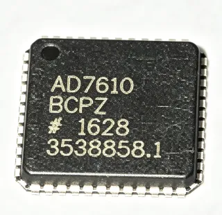
AD9265 - 16-Bit 125 MSPS ADC | Analog Devices | Communications
MPN: AD9265 ✓ Active| Qty | Unit Price | Extended |
|---|---|---|
| 1 | $45.32 | $45.32 |
| 10 | $41.87 | $418.70 |
| 100 | $36.54 | $3,654.00 |
| 500 | $32.1 | $16,050.00 |
| 1,000 | $28.75 | $28,750.00 |
AD9265 Overview
An analog-to-digital converter (ADC) is a critical component in signal processing chains, converting continuous analog signals into discrete digital values for processing by digital systems. The AD9265 belongs to the family of high-speed, high-resolution ADCs, which are essential in applications such as software-defined radios, radar systems, and medical imaging. Its 16-bit resolution and 125 MSPS sampling rate enable precise digitization of wideband signals, balancing speed and accuracy.
Key features of the AD9265 include a 16-bit resolution, sampling rates of 125 MSPS, 105 MSPS, and 80 MSPS variants, and a 1.8 V supply voltage. It offers high SNR and SFDR, making it ideal for demanding communications systems. The device also includes a differential input, a CMOS or LVDS output interface, and a flexible SPI port for configuration. Its low power dissipation and small package footprint enhance system integration.
Technically, the AD9265 employs a pipelined ADC architecture, which allows high-speed conversion while maintaining high resolution. The device integrates a sample-and-hold amplifier, a reference voltage, and digital error correction, ensuring accurate conversion across the full input range. The output data can be formatted in either offset binary or two's complement, providing flexibility for various digital interfaces.
Typical applications include communications receivers, radar systems, medical ultrasound, and test and measurement equipment. In communications, the AD9265's high SNR and SFDR enable reliable demodulation of complex modulated signals. In radar, its high sampling rate captures fast-rising pulses with precision. In medical imaging, the 16-bit resolution ensures fine detail in ultrasound images.
When designing with the AD9265, ensure proper decoupling of the analog and digital supplies, and use a low-jitter clock source to maximize SNR. The differential input should be driven with a balanced source to achieve optimal performance. The SPI port allows adjustment of output format and test modes, which can be used to verify system integrity.
Drop-in alternatives for AD9265 — same package, pin-to-pin compatible. Different-package parts requiring PCB rework are excluded.
Quick Comparison Tool — Select alternative parts for side-by-side comparison:
AD9265BCPZ-105
✅ Drop-In📋 Reference alternative (not in catalog)
AD9265BCPZ-125
✅ Drop-In📋 Reference alternative (not in catalog)
AD9265BCPZ-80
✅ Drop-In ⚠️ Specs Unverified📋 Reference alternative (not in catalog)
LTC2208
✅ Drop-In ⚠️ Specs Unverified📋 Reference alternative (not in catalog)
ADS4249
✅ Drop-In ⚠️ Specs Unverified📋 Reference alternative (not in catalog)
AD9265 Maximum Ratings & Electrical Characteristics
| Resolution | 16 bits |
| Sampling Rate | 125 MSPS (also 105 MSPS, 80 MSPS variants) |
| Number of Inputs | 1 |
| Input Type | Differential |
| Data Interface | CMOS or LVDS |
| Architecture | Pipelined |
| Supply Voltage | 1.8 V |
| Package | 48-LFCSP-VQ (7x7 mm) |
| Mounting Type | Surface Mount |
| RoHS Status | Compliant |
| Number of Converters | 1 |
AD9265 Pin Configuration
| Pin 1 | AVDD — Analog supply voltage (1.8 V) |
| Pin 2 | VIN+ — Positive differential analog input |
| Pin 3 | VIN- — Negative differential analog input |
| Pin 4 | AVSS — Analog ground |
| Pin 5 | CLK+ — Positive clock input |
| Pin 6 | CLK- — Negative clock input |
| Pin 7 | DVDD — Digital supply voltage (1.8 V) |
| Pin 8 | DVSS — Digital ground |
| Pin 9 | D0 — Digital output bit 0 (LSB) |
| Pin 10 | D1 — Digital output bit 1 |
| Pin 11 | D2 — Digital output bit 2 |
| Pin 12 | D3 — Digital output bit 3 |
| Pin 13 | D4 — Digital output bit 4 |
| Pin 14 | D5 — Digital output bit 5 |
| Pin 15 | D6 — Digital output bit 6 |
| Pin 16 | D7 — Digital output bit 7 |
| Pin 17 | D8 — Digital output bit 8 |
| Pin 18 | D9 — Digital output bit 9 |
| Pin 19 | D10 — Digital output bit 10 |
| Pin 20 | D11 — Digital output bit 11 |
| Pin 21 | D12 — Digital output bit 12 |
| Pin 22 | D13 — Digital output bit 13 |
| Pin 23 | D14 — Digital output bit 14 |
| Pin 24 | D15 — Digital output bit 15 (MSB) |
| Pin 25 | SCLK — SPI clock input |
| Pin 26 | SDIO — SPI data input/output |
| Pin 27 | CSB — SPI chip select (active low) |
| Pin 28 | PDWN — Power-down control (active high) |
| Pin 29 | SYNC — Synchronization input |
| Pin 30 | OEB — Output enable (active low) |
| Pin 31 | VREF — Voltage reference output |
| Pin 32 | SENSE — Reference mode select |
| Pin 33 | REFB — Reference bottom |
| Pin 34 | REFT — Reference top |
| Pin 35 | CML — Common-mode level output |
| Pin 36 | VCM — Common-mode voltage output |
| Pin 37 | AVDD — Analog supply voltage (1.8 V) |
| Pin 38 | AVSS — Analog ground |
| Pin 39 | AVSS — Analog ground |
| Pin 40 | AVDD — Analog supply voltage (1.8 V) |
| Pin 41 | DVDD — Digital supply voltage (1.8 V) |
| Pin 42 | DVSS — Digital ground |
| Pin 43 | DVSS — Digital ground |
| Pin 44 | DVDD — Digital supply voltage (1.8 V) |
| Pin 45 | NC — No connect |
| Pin 46 | NC — No connect |
| Pin 47 | NC — No connect |
| Pin 48 | NC — No connect |
Typical Applications
AD9265 is suitable for 6 applications: Communications Receivers, Radar Systems, Medical Ultrasound, Test and Measurement, Software-Defined Radio, Communications Infrastructure.
Communications Receivers
The AD9265 is ideal for communications receivers due to its high SNR and SFDR, enabling reliable demodulation of complex modulated signals. Its 125 MSPS sampling rate supports wideband signals, and the 16-bit resolution ensures high dynamic range. The device's low power consumption is beneficial for multi-channel systems. In a typical receiver chain, the AD9265 digitizes the IF signal after downconversion, providing a digital output for baseband processing. The differential input and LVDS output interface simplify connection to FPGAs or DSPs. The SPI port allows configuration of output format and test modes, enhancing system flexibility.
Recommended
Radar Systems
In radar systems, the AD9265's high sampling rate and 16-bit resolution enable precise digitization of radar returns, improving target detection and range resolution. The device's high SFDR minimizes spurious signals that could be mistaken for targets. The 1.8 V supply and low power dissipation are advantageous for phased-array radar modules. The AD9265 can be used in both pulsed and continuous-wave radar architectures. Its pipelined architecture ensures low latency, which is critical for real-time processing. The LVDS output interface provides high-speed data transfer to processing units.
Recommended
Medical Ultrasound
The AD9265 is well-suited for medical ultrasound systems, where high resolution and low noise are essential for image quality. The 16-bit resolution provides fine amplitude detail, while the 125 MSPS sampling rate captures high-frequency ultrasound echoes. The device's low power consumption is important for portable ultrasound devices. In an ultrasound receiver, the AD9265 digitizes the echo signal after beamforming, enabling digital signal processing for image reconstruction. The differential input reduces common-mode noise, improving signal integrity. The SPI port allows adjustment of output data format to match the processing chain.
Recommended
Test and Measurement
The AD9265 is used in test and measurement equipment such as oscilloscopes and spectrum analyzers, where high bandwidth and accuracy are required. Its 125 MSPS sampling rate and 16-bit resolution enable precise digitization of signals up to tens of MHz. The device's high SNR ensures accurate measurements of small signals. In a digital oscilloscope, the AD9265 digitizes the input signal after attenuation and amplification, providing a digital representation for display and analysis. The LVDS output interface supports high-speed data transfer to the acquisition system. The SPI port enables configuration of test modes for calibration.
Recommended
Software-Defined Radio
The AD9265 is a key component in software-defined radios (SDR), where it digitizes wideband RF signals for digital processing. Its high sampling rate and 16-bit resolution enable the capture of multiple channels simultaneously. The device's high SFDR ensures that weak signals are not masked by spurious tones. In an SDR receiver, the AD9265 digitizes the IF signal after downconversion, allowing flexible demodulation in software. The LVDS output interface provides a high-speed digital stream to an FPGA or DSP. The SPI port allows dynamic reconfiguration of the ADC for different operating modes.
Recommended
Communications Infrastructure
The AD9265 is used in communications infrastructure such as base stations and microwave links, where high performance and reliability are critical. Its 16-bit resolution and 125 MSPS sampling rate support high-capacity data transmission. The device's low power consumption reduces heat dissipation in dense equipment. In a base station receiver, the AD9265 digitizes multiple carriers simultaneously, enabling digital predistortion and interference cancellation. The differential input and LVDS output interface simplify connection to digital processors. The SPI port allows configuration of output data format and test modes for system calibration.
Recommended
Recommended Products Summary
Engineering reference data for AD9265 — comparison, design guidance, and compliance information.
Selection Guide
Comparison with Alternatives
| Parameter | This Product | AD9265BCPZ-105 | AD9265BCPZ-125 | AD9265BCPZ-80 | LTC2208 | ADS4249 |
|---|---|---|---|---|---|---|
| Package | 48-LFCSP-VQ (7x7) | 48-LFCSP-VQ (7x7) | 48-LFCSP-VQ (7x7) | 48-LFCSP-VQ (7x7) | 48-LFCSP-VQ (7x7) | 48-LFCSP-VQ (7x7) |
| Brand | Analog Devices | Analog Devices | Analog Devices | Analog Devices | Analog Devices | Texas Instruments |
| Resolution | 16 bits | 16 bits | 16 bits | 16 bits | 16 bits | 16 bits |
| Sampling Rate | 125 MSPS | 105 MSPS | 125 MSPS | 80 MSPS | 130 MSPS | 250 MSPS |
| Supply Voltage | 1.8 V | 1.8 V | 1.8 V | 1.8 V | 1.8 V | 1.8 V |
| Input Type | Differential | Differential | Differential | Differential | Differential | Differential |
| Data Interface | CMOS or LVDS | CMOS or LVDS | CMOS or LVDS | CMOS or LVDS | LVDS | LVDS |
| Architecture | Pipelined | Pipelined | Pipelined | Pipelined | Pipelined | Pipelined |
Key Differentiators
- High sampling rate with 16-bit resolution (vs AD9265BCPZ-105)
- Low power consumption (vs LTC2208)
- Flexible output interface (vs ADS4249)
Design Notes
The AD9265 requires a clean 1.8 V supply for both analog and digital domains. Use separate analog and digital supply pins with proper decoupling. Place 0.1 uF and 10 uF capacitors close to each supply pin to filter high-frequency noise. A ferrite bead can be used to isolate the analog supply from digital switching noise.
For optimal performance, use a solid ground plane and partition the PCB into analog and digital sections. The analog input traces should be kept short and shielded to minimize noise pickup. The clock input should be routed with controlled impedance and kept away from digital outputs to avoid crosstalk.
The differential analog input should be driven with a balanced source to achieve the best SNR and SFDR. Use a transformer or a differential amplifier to convert single-ended signals to differential. Ensure the common-mode voltage is set to the specified VCM level. The clock source must have low jitter to avoid degrading the SNR.
Compliance Information
RoHS compliant per Analog Devices product page. No AEC-Q100 qualification for this ADC.