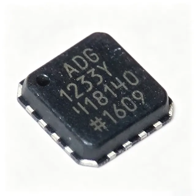
ADG1233YCPZ-REEL7 - Triple SPDT Analog Switch | Analog Devices
MPN: ADG1233YCPZ-REEL7 ✓ Active| Qty | Unit Price | Extended |
|---|---|---|
| 1 | $22.0909 | $22.09 |
| 10 | $15.9545 | $159.55 |
| 100 | $14.1136 | $1,411.36 |
| 500 | $13.5 | $6,750.00 |
| 1,000 | $12.8864 | $12,886.40 |
ADG1233YCPZ-REEL7 Overview
An analog switch is a semiconductor device that selectively connects or disconnects an analog signal path under digital control. It is a fundamental building block in signal routing, multiplexing, and sample-and-hold circuits. The ADG1233 belongs to the family of analog switches and multiplexers, which are part of the broader category of interface ICs and signal conditioning components. Its iCMOS® (industrial CMOS) process technology ensures low power consumption and high voltage handling, bridging the gap between traditional CMOS and higher-voltage bipolar processes.
Key features include break-before-make switching action, which prevents momentary shorting when switching channels, and an EN input that enables or disables the entire device. The switch is fully specified with 3 V logic-compatible inputs, allowing direct interface with low-voltage digital controllers. Rail-to-rail operation ensures minimal signal distortion across the full supply range. The 1.5 pF off capacitance and 0.5 pC charge injection minimize signal degradation in high-frequency and precision applications.
The ADG1233 utilizes a proprietary iCMOS® process that combines the advantages of high-voltage CMOS with low power dissipation. This architecture enables the device to handle ±15 V supplies while maintaining low leakage currents and fast switching speeds. The break-before-make action is implemented through internal timing circuitry, ensuring reliable channel isolation during transitions. The device is available in a 16-lead LFCSP-VQ package, which offers excellent thermal performance and a small footprint for space-constrained designs.
Typical applications include audio signal routing, precision data acquisition systems, automatic test equipment (ATE), and medical instrumentation. The low capacitance and charge injection make it particularly suitable for high-speed analog signals, while the wide supply range accommodates both bipolar and single-supply designs. The EN pin provides a convenient means of power-down or signal isolation in multi-channel systems.
When designing with the ADG1233, ensure that the digital control signals are within the specified logic thresholds and that the supply voltages are properly decoupled with 0.1 µF capacitors close to the VDD and VSS pins. The break-before-make feature eliminates the need for external timing circuits, but the user should verify that the switching time meets system requirements.
Drop-in alternatives for ADG1233YCPZ-REEL7 — same package, pin-to-pin compatible. Different-package parts requiring PCB rework are excluded.
Quick Comparison Tool — Select alternative parts for side-by-side comparison:
ADG1233YCPZ-REEL
📋 Reference alternative (not in catalog)
ADG1234YCPZ-REEL7
📋 Reference alternative (not in catalog)
ADG1213YCPZ-REEL7
📋 Reference alternative (not in catalog)
ADG1433YCPZ-REEL7
📋 Reference alternative (not in catalog)
MAX14759EUE+
📋 Reference alternative (not in catalog)
ADG1233YCPZ-REEL7 Maximum Ratings & Electrical Characteristics
| Number of Circuits | 3 |
| Switch Configuration | SPDT |
| On-State Resistance (Max) | 190 Ω |
| Supply Voltage Range | ±15 V or +12 V |
| Off Capacitance | 1.5 pF |
| Charge Injection | 0.5 pC |
| Logic-Compatible Inputs | 3 V |
| Break-Before-Make | Yes |
| Enable Input | Yes |
| Operating Temperature Range | -40°C to +125°C |
| Package | 16-LFCSP-VQ (4x4 mm) |
| Mounting Type | Surface Mount |
| RoHS Status | Compliant |
| Technology | iCMOS® |
ADG1233YCPZ-REEL7 Pin Configuration
| Pin 1 | S1A — Source terminal for switch 1, channel A |
| Pin 2 | D1 — Drain terminal for switch 1 |
| Pin 3 | S1B — Source terminal for switch 1, channel B |
| Pin 4 | GND — Ground |
| Pin 5 | S2A — Source terminal for switch 2, channel A |
| Pin 6 | D2 — Drain terminal for switch 2 |
| Pin 7 | S2B — Source terminal for switch 2, channel B |
| Pin 8 | EN — Enable input (active high) |
| Pin 9 | S3A — Source terminal for switch 3, channel A |
| Pin 10 | D3 — Drain terminal for switch 3 |
| Pin 11 | S3B — Source terminal for switch 3, channel B |
| Pin 12 | VSS — Negative supply voltage |
| Pin 13 | IN1 — Digital control input for switch 1 |
| Pin 14 | IN2 — Digital control input for switch 2 |
| Pin 15 | IN3 — Digital control input for switch 3 |
| Pin 16 | VDD — Positive supply voltage |
Typical Applications
ADG1233YCPZ-REEL7 is suitable for 6 applications: Audio Signal Routing, Data Acquisition Systems, Automatic Test Equipment (ATE), Medical Instrumentation, Precision Instrumentation, Communication Systems.
Audio Signal Routing
The ADG1233YCPZ-REEL7 is ideal for audio signal routing due to its low on-resistance (120 Ω) and low charge injection (0.5 pC), which minimize signal distortion. It can be used in mixing consoles, effects processors, and audio test equipment to switch between multiple audio sources without introducing audible clicks or pops. The break-before-make action ensures clean transitions, and the wide supply range accommodates both bipolar and single-supply audio circuits. Its small LFCSP package saves board space in compact audio devices.
Recommended
Data Acquisition Systems
In data acquisition systems, the ADG1233YCPZ-REEL7 provides precise signal routing with low off capacitance (1.5 pF) and charge injection (0.5 pC), preserving signal integrity. It can multiplex multiple sensor inputs to a single ADC, reducing component count. The 3 V logic-compatible inputs simplify interfacing with microcontrollers. The wide supply range (±15 V) allows direct connection to industrial sensors. Its break-before-make action prevents channel crosstalk during switching, ensuring accurate measurements.
Recommended
Automatic Test Equipment (ATE)
The ADG1233YCPZ-REEL7 is well-suited for ATE applications where high channel density and low leakage are critical. Its low off capacitance (1.5 pF) minimizes signal degradation in high-frequency test signals. The device's fast switching and break-before-make action enable reliable routing of test signals to multiple points. The EN pin allows global disable for power saving or isolation. The small LFCSP package enables dense PCB layouts, and the wide supply range supports various test signal levels.
Recommended
Medical Instrumentation
In medical instrumentation, the ADG1233YCPZ-REEL7 ensures accurate signal routing with low charge injection (0.5 pC) and low leakage, which is essential for biopotential measurements. It can be used in ECG, EEG, and patient monitoring systems to switch between multiple electrodes. The device's low power consumption and small footprint are advantageous for portable devices. The wide supply range and rail-to-rail operation ensure compatibility with various analog front-end designs.
Recommended
Precision Instrumentation
The ADG1233YCPZ-REEL7 is ideal for precision instrumentation such as digital multimeters and source measure units. Its low off capacitance (1.5 pF) and charge injection (0.5 pC) minimize errors in high-impedance circuits. The break-before-make action prevents transient glitches during range switching. The device's low on-resistance (120 Ω) reduces voltage drop, and the wide supply range supports both high-voltage and low-voltage measurements. The EN pin allows for power-down in battery-operated instruments.
Recommended
Communication Systems
In communication systems, the ADG1233YCPZ-REEL7 provides low-distortion signal routing for RF and IF paths. Its low off capacitance (1.5 pF) minimizes signal coupling, and the break-before-make action ensures clean switching in TDD systems. The device can be used in base stations, software-defined radios, and test equipment. The 3 V logic-compatible inputs simplify control from FPGAs or DSPs. The wide supply range and rail-to-rail operation support various signal levels.
Recommended
Recommended Products Summary
Engineering reference data for ADG1233YCPZ-REEL7 — comparison, design guidance, and compliance information.
Selection Guide
Comparison with Alternatives
| Parameter | This Product | ADG1233YCPZ-REEL | ADG1234YCPZ-REEL7 | ADG1213YCPZ-REEL7 | ADG1433YCPZ-REEL7 |
|---|---|---|---|---|---|
| Package | 16-LFCSP-VQ (4x4 mm) | 16-LFCSP-VQ (4x4 mm) | 16-LFCSP-VQ (4x4 mm) | 16-LFCSP-VQ (4x4 mm) | 16-LFCSP-VQ (4x4 mm) |
| Brand | Analog Devices | Analog Devices | Analog Devices | Analog Devices | Analog Devices |
| Number of Circuits | 3 | 3 | 4 | 3 | 3 |
| On-Resistance (Max) | 190 Ω | 190 Ω | 190 Ω | 1.2 Ω | 190 Ω |
| Off Capacitance | 1.5 pF | 1.5 pF | 1.5 pF | 1.5 pF | 1.5 pF |
| Charge Injection | 0.5 pC | 0.5 pC | 0.5 pC | 0.5 pC | 0.5 pC |
| Supply Voltage Range | ±15 V or +12 V | ±15 V or +12 V | ±15 V or +12 V | ±15 V or +12 V | ±20 V |
| Logic-Compatible Inputs | 3 V | 3 V | 3 V | 3 V | 3 V |
Key Differentiators
- Ultra-low off capacitance of 1.5 pF (vs ADG1213YCPZ-REEL7)
- Break-before-make switching action (vs ADG1234YCPZ-REEL7)
- Wide supply range of ±15 V (vs ADG1433YCPZ-REEL7)
Design Notes
Ensure that the VDD and VSS pins are properly decoupled with 0.1 µF ceramic capacitors placed as close to the pins as possible. For dual-supply operation, use a 10 µF tantalum capacitor in parallel for bulk decoupling. The supply voltage should not exceed the absolute maximum ratings of ±17 V or +13 V for single supply.
For optimal performance, route the analog signal traces away from digital control lines to minimize crosstalk. Use a ground plane under the device to reduce parasitic inductance. The LFCSP package has an exposed pad that should be soldered to the PCB ground for improved thermal performance.
Do not apply voltages to the source or drain pins that exceed the supply rails, as this can cause latch-up. Ensure that the digital control signals are within the specified logic thresholds (VIH = 2.0 V, VIL = 0.8 V for 3 V logic). The EN pin should be tied to VDD if not used, to keep the device enabled.
Compliance Information
RoHS compliant per Analog Devices product page. Not AEC-Q100 qualified.


