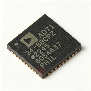
AD9268 - Dual 16-Bit 125 MSPS ADC | Analog Devices
MPN: AD9268 ✓ Active| Qty | Unit Price | Extended |
|---|---|---|
| 1 | $45.32 | $45.32 |
| 10 | $41.87 | $418.70 |
| 100 | $36.54 | $3,654.00 |
| 500 | $32.1 | $16,050.00 |
| 1,000 | $28.75 | $28,750.00 |
AD9268 Overview
An analog-to-digital converter (ADC) is a critical building block in signal processing chains, converting continuous analog signals into discrete digital values for processing by DSPs, FPGAs, or microcontrollers. The AD9268 belongs to the family of high-speed, high-resolution ADCs, positioned between lower-speed precision converters and ultra-high-speed RF-sampling converters. Its dual-channel architecture enables simultaneous sampling of two signals, which is essential for I/Q demodulation in communications receivers and for multi-phase monitoring in industrial systems.
Key features of the AD9268 include a 16-bit resolution with a maximum sample rate of 125 MSPS, a spurious-free dynamic range (SFDR) of 90 dBc, and a signal-to-noise ratio (SNR) of 78 dBFS. The device supports both 1.8 V and 3.3 V digital output levels, and its power dissipation is typically 1.2 W at 125 MSPS. The AD9268 is pin-compatible with the AD9258 (14-bit), allowing a simple migration path between resolutions. It also shares pin compatibility with the AD9251, AD9231, and AD9204 families for lower sample rate, low-power applications.
Technically, the AD9268 uses a multi-stage pipelined architecture with digital error correction, achieving high linearity and low noise. The internal voltage reference can be overridden via the SENSE pin for external reference operation, providing flexibility in gain and full-scale range settings. The device includes a clock duty cycle stabilizer, which maintains performance even with non-50% duty cycle clocks, and a data output format selectable between offset binary and twos complement.
Typical applications include communications receivers (cellular base stations, point-to-point microwave links), radar systems, medical imaging (ultrasound), and industrial data acquisition. The dual-channel capability makes it ideal for diversity reception and I/Q demodulation, where two channels must be sampled simultaneously with matched performance.
When designing with the AD9268, ensure a clean, low-jitter clock source to achieve the specified SNR and SFDR. The analog input should be driven with a differential amplifier or balun to optimize performance, and the power supply pins should be decoupled with 0.1 uF and 10 uF capacitors. The device is available in a 64-lead LFCSP package, which provides excellent thermal performance and a compact footprint.
Drop-in alternatives for AD9268 — same package, pin-to-pin compatible. Different-package parts requiring PCB rework are excluded.
Quick Comparison Tool — Select alternative parts for side-by-side comparison:
AD9258
✅ Drop-In📋 Reference alternative (not in catalog)
AD9251
✅ Drop-In📋 Reference alternative (not in catalog)
AD9231
✅ Drop-In📋 Reference alternative (not in catalog)
AD9204
✅ Drop-In📋 Reference alternative (not in catalog)
SC9268
✅ Drop-In ⚠️ Specs Unverified📋 Reference alternative (not in catalog)
GX9268
✅ Drop-In ⚠️ Specs Unverified📋 Reference alternative (not in catalog)
AD9268 Maximum Ratings & Electrical Characteristics
| Resolution | 16 bits |
| Number of Channels | 2 (dual) |
| Sampling Rate | 80 MSPS / 105 MSPS / 125 MSPS |
| Input Type | Differential |
| Data Interface | Parallel CMOS / LVDS |
| Supply Voltage | 1.8 V (analog), 1.8 V / 3.3 V (digital) |
| SNR | 78 dBFS (typical) |
| SFDR | 90 dBc (typical) |
| Power Dissipation | 1.2 W (typical at 125 MSPS) |
| Operating Temperature Range | -40°C to +85°C |
| Package | 64-lead LFCSP (9x9 mm) |
| Mounting Type | Surface Mount |
| Reference Type | Internal / External |
| RoHS Status | Compliant |
| Pin Compatibility | AD9258, AD9251, AD9231, AD9204 |
AD9268 Pin Configuration
| Pin 1 | AVDD — Analog power supply (1.8 V) |
| Pin 2 | AVSS — Analog ground |
| Pin 3 | VIN+ — Positive differential analog input |
| Pin 4 | VIN- — Negative differential analog input |
| Pin 5 | AVSS — Analog ground |
| Pin 6 | SENSE — Reference mode selection |
| Pin 7 | REF — Voltage reference output/input |
| Pin 8 | AVDD — Analog power supply (1.8 V) |
| Pin 9 | CLK+ — Positive differential clock input |
| Pin 10 | CLK- — Negative differential clock input |
| Pin 11 | AVSS — Analog ground |
| Pin 12 | DRVDD — Digital output driver supply (1.8 V or 3.3 V) |
| Pin 13 | DRVSS — Digital ground |
| Pin 14 | D0A — Digital output bit 0 (Channel A) |
| Pin 15 | D1A — Digital output bit 1 (Channel A) |
| Pin 16 | D2A — Digital output bit 2 (Channel A) |
| Pin 17 | D3A — Digital output bit 3 (Channel A) |
| Pin 18 | D4A — Digital output bit 4 (Channel A) |
| Pin 19 | D5A — Digital output bit 5 (Channel A) |
| Pin 20 | D6A — Digital output bit 6 (Channel A) |
| Pin 21 | D7A — Digital output bit 7 (Channel A) |
| Pin 22 | D8A — Digital output bit 8 (Channel A) |
| Pin 23 | D9A — Digital output bit 9 (Channel A) |
| Pin 24 | D10A — Digital output bit 10 (Channel A) |
| Pin 25 | D11A — Digital output bit 11 (Channel A) |
| Pin 26 | D12A — Digital output bit 12 (Channel A) |
| Pin 27 | D13A — Digital output bit 13 (Channel A) |
| Pin 28 | D14A — Digital output bit 14 (Channel A) |
| Pin 29 | D15A — Digital output bit 15 (Channel A) |
| Pin 30 | DRVSS — Digital ground |
| Pin 31 | DRVDD — Digital output driver supply |
| Pin 32 | D0B — Digital output bit 0 (Channel B) |
| Pin 33 | D1B — Digital output bit 1 (Channel B) |
| Pin 34 | D2B — Digital output bit 2 (Channel B) |
| Pin 35 | D3B — Digital output bit 3 (Channel B) |
| Pin 36 | D4B — Digital output bit 4 (Channel B) |
| Pin 37 | D5B — Digital output bit 5 (Channel B) |
| Pin 38 | D6B — Digital output bit 6 (Channel B) |
| Pin 39 | D7B — Digital output bit 7 (Channel B) |
| Pin 40 | D8B — Digital output bit 8 (Channel B) |
| Pin 41 | D9B — Digital output bit 9 (Channel B) |
| Pin 42 | D10B — Digital output bit 10 (Channel B) |
| Pin 43 | D11B — Digital output bit 11 (Channel B) |
| Pin 44 | D12B — Digital output bit 12 (Channel B) |
| Pin 45 | D13B — Digital output bit 13 (Channel B) |
| Pin 46 | D14B — Digital output bit 14 (Channel B) |
| Pin 47 | D15B — Digital output bit 15 (Channel B) |
| Pin 48 | DRVSS — Digital ground |
| Pin 49 | DRVDD — Digital output driver supply |
| Pin 50 | PDWN — Power-down control (active high) |
| Pin 51 | DFS — Data format select (offset binary / twos complement) |
| Pin 52 | OEB — Output enable for Channel B (active low) |
| Pin 53 | OEA — Output enable for Channel A (active low) |
| Pin 54 | AVSS — Analog ground |
| Pin 55 | AVDD — Analog power supply (1.8 V) |
| Pin 56 | VREF — Voltage reference output |
| Pin 57 | AVSS — Analog ground |
| Pin 58 | AVDD — Analog power supply (1.8 V) |
| Pin 59 | VIN+B — Positive differential analog input (Channel B) |
| Pin 60 | VIN-B — Negative differential analog input (Channel B) |
| Pin 61 | AVSS — Analog ground |
| Pin 62 | AVDD — Analog power supply (1.8 V) |
| Pin 63 | NC — No connect |
| Pin 64 | EPAD — Exposed pad (thermal and ground) |
Typical Applications
AD9268 is suitable for 6 applications: Communications Receivers, Radar Systems, Medical Imaging (Ultrasound), Industrial Data Acquisition, Test and Measurement, Wireless Infrastructure.
Communications Receivers
The AD9268's dual 16-bit channels and high sample rate up to 125 MSPS make it ideal for I/Q demodulation in cellular base stations and microwave links. Its 78 dBFS SNR and 90 dBc SFDR ensure excellent signal fidelity for multi-carrier reception. The device's pin compatibility with the AD9258 allows easy migration between 16-bit and 14-bit designs. In a typical receiver, the AD9268 digitizes the analog I and Q signals from the downconverter, enabling digital processing for channel filtering and demodulation. The high SFDR minimizes intermodulation distortion, which is critical in crowded spectrum environments. Power dissipation of 1.2 W is acceptable for base station equipment, and the small LFCSP package saves board space.
Recommended
Radar Systems
In radar systems, the AD9268 provides high-speed dual-channel digitization for I/Q processing of return signals. Its 16-bit resolution and 125 MSPS sample rate capture fine amplitude and phase details, improving target detection and range resolution. The device's low noise and high SFDR are essential for distinguishing weak echoes from clutter. The dual channels enable simultaneous sampling of two polarizations or two antenna elements, enhancing system performance. The AD9268's wide operating temperature range (-40°C to +85°C) suits rugged military and aerospace environments. Its power dissipation is manageable with proper thermal design, and the LFCSP package is suitable for compact radar modules.
Recommended
Medical Imaging (Ultrasound)
The AD9268 is well-suited for ultrasound systems, where dual-channel, high-resolution ADC conversion is required for beamforming and image processing. Its 16-bit resolution provides fine amplitude resolution for detecting subtle tissue differences, while the 125 MSPS sample rate supports high-frequency transducers. The device's low noise performance ensures clear images with minimal artifacts. The dual channels allow simultaneous processing of multiple transducer elements, improving frame rates. The AD9268's small package and low power consumption are advantageous for portable ultrasound devices. Its pin compatibility with other ADI ADCs offers design flexibility for different system configurations.
Recommended
Industrial Data Acquisition
In industrial data acquisition systems, the AD9268 provides high-speed, high-resolution conversion for monitoring and control applications. Its dual channels enable simultaneous sampling of two signals, such as voltage and current, for power monitoring or motor control. The 16-bit resolution ensures accurate measurement of small signal variations, while the 125 MSPS sample rate captures fast transients. The device's robust design operates over a wide temperature range, making it suitable for harsh industrial environments. The AD9268's low power dissipation reduces thermal stress in enclosed systems. Its flexible digital interface (CMOS or LVDS) simplifies integration with FPGAs or DSPs.
Recommended
Test and Measurement
The AD9268 is used in oscilloscopes, spectrum analyzers, and other test equipment requiring high-speed, high-resolution digitization. Its dual channels allow simultaneous acquisition of two signals, useful for differential measurements or two-channel scopes. The 16-bit resolution and 125 MSPS sample rate provide detailed waveform capture with high dynamic range. The device's low noise and high SFDR ensure accurate measurement of small signals in the presence of large ones. The AD9268's small package and low power consumption are beneficial for portable instruments. Its pin compatibility with other ADI ADCs allows designers to offer multiple product variants with minimal redesign.
Recommended
Wireless Infrastructure
The AD9268 is ideal for wireless infrastructure such as small cells and remote radio heads (RRHs). Its dual 16-bit channels and high sample rate support multi-carrier GSM/WCDMA/LTE reception. The device's high SFDR and SNR ensure compliance with stringent spectral emission masks. The AD9268's low power consumption is critical for RRHs where heat dissipation is limited. Its small LFCSP package enables compact radio designs. The device's pin compatibility with the AD9258 allows a straightforward upgrade path from 14-bit to 16-bit resolution. The AD9268 also supports external reference operation for gain calibration, enhancing system flexibility.
Recommended
Recommended Products Summary
Engineering reference data for AD9268 — comparison, design guidance, and compliance information.
Selection Guide
Comparison with Alternatives
| Parameter | This Product | AD9258 | AD9251 | AD9231 | AD9204 | SC9268 | GX9268 |
|---|---|---|---|---|---|---|---|
| Package | 64-lead LFCSP | 64-lead LFCSP | 64-lead LFCSP | 64-lead LFCSP | 64-lead LFCSP | 64-lead LFCSP | 64-lead LFCSP |
| Brand | Analog Devices | Analog Devices | Analog Devices | Analog Devices | Analog Devices | SGMC | GXSC |
| Resolution | 16 bits | 14 bits | 14 bits | 12 bits | 12 bits | 16 bits | 16 bits |
| Max Sample Rate | 125 MSPS | 125 MSPS | 40 MSPS | 40 MSPS | 40 MSPS | 125 MSPS | 125 MSPS |
| SNR | 78 dBFS | 74 dBFS | 74 dBFS | 70 dBFS | 70 dBFS | 78 dBFS | 78 dBFS |
| SFDR | 90 dBc | 88 dBc | 85 dBc | 82 dBc | 82 dBc | 90 dBc | 90 dBc |
| Power Dissipation | 1.2 W | 1.1 W | 0.5 W | 0.4 W | 0.4 W | 1.2 W | 1.2 W |
| Supply Voltage | 1.8 V | 1.8 V | 1.8 V | 1.8 V | 1.8 V | 1.8 V | 1.8 V |
| Pin Compatibility | Yes (with AD9258, AD9251, AD9231, AD9204) | Yes | Yes | Yes | Yes | Yes | Yes |
Key Differentiators
- 16-bit resolution with 125 MSPS sample rate (vs AD9258)
- Pin-compatible with multiple ADI ADCs (vs AD9251)
- High SFDR of 90 dBc (vs AD9231)
Design Notes
The AD9268 requires a clean 1.8 V analog supply (AVDD) and a separate digital supply (DRVDD) that can be 1.8 V or 3.3 V. Decouple each supply pin with a 0.1 uF ceramic capacitor placed as close as possible to the pin, and a 10 uF bulk capacitor on the board. Use a low-noise LDO for AVDD to minimize supply-induced noise, which can degrade SNR. The power dissipation of 1.2 W at 125 MSPS should be considered in thermal design; the exposed pad (EPAD) must be soldered to a ground plane for effective heat sinking.
For optimal performance, use a solid ground plane under the AD9268 and split analog and digital ground planes only if necessary, connecting them at a single point. The analog input traces should be routed as differential pairs with controlled impedance (typically 100 ohms differential) and kept as short as possible. Place the input drive amplifier (e.g., ADL5565) close to the ADC to minimize parasitic capacitance. The clock input should also be routed as a differential pair with 50-ohm single-ended impedance, and the clock source should have low jitter to achieve the specified SNR. Avoid routing digital output traces near the analog input to prevent coupling.
A common mistake is driving the analog input single-ended, which degrades SFDR and SNR. Always use a differential drive circuit, such as a balun or differential amplifier. Another pitfall is using a noisy clock source; the AD9268's SNR is directly affected by clock jitter, so use a low-jitter clock (e.g., from a crystal oscillator or a dedicated clock buffer like ADCLK905). Ensure the SENSE pin is correctly configured for the desired reference mode; leaving it floating may result in unexpected full-scale range. Also, do not exceed the absolute maximum ratings on any pin, especially the analog input, which could damage the device.
Compliance Information
RoHS compliant per Analog Devices product page. Not AEC-Q100 qualified; for automotive, consider AD9268-125EBZ evaluation board for testing.