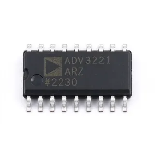
DG212CY+ - Quad SPST 175Ω Analog Switch | Analog Devices
MPN: DG212CY+ ✓ ActiveDG212CY+ Overview
An analog switch is an integrated semiconductor device that connects or disconnects signal paths under logic control. The DG212CY+ belongs to the analog switch hierarchy, where it complements multiplexers, demultiplexers, and matrix switchers. Its four SPST channels can isolate instrumentation inputs, route test signals, select external circuits, or provide break-before-make functions when driven by suitable control logic.
The DG212 family uses low-cost monolithic CMOS circuitry and normally open contacts. Four independently controlled switches reduce external component count in systems requiring several signal connections. The maximum specified on-resistance is 175 Ω, making the device suitable for moderate-impedance signals rather than low-ohm precision measurement paths. Its 16-lead SOIC format supports conventional surface-mount assembly.
The DG212CY+ can operate continuously with positive and negative supply rails from ±4.5 V to ±18 V. Analog Devices specifies latch-up-free behavior when the supply rails are disconnected while input signals remain connected. This feature helps avoid unintended current paths during power-down conditions. Control polarity distinguishes the DG212 from related DG211 devices, so control-logic compatibility must be checked before substitution.
Typical uses include communications equipment, instrumentation, process-control systems, computer peripherals, automated test equipment, and signal-isolation circuits. The device is especially useful when multiple low-bandwidth or moderate-impedance paths must be selected independently. Its four channels can route sensor lines, select measurement sources, or disconnect external equipment from a shared bus.
Layout should keep switched traces short and provide a low-impedance ground reference around the device. Input and output pins must remain within the absolute maximum ratings of the manufacturer datasheet, and unused control inputs should be driven to a defined logic state. Verify signal amplitude, supply polarity, control levels, and acceptable switching transients before finalizing the analog path.
This product page combines the manufacturer’s switch description with practical substitution, comparison, and PCB-design guidance. It focuses on the electrical limits, control compatibility, package footprint, and application constraints that determine whether DG212CY+ is appropriate for a new design or an existing instrumentation and control board.
Drop-in alternatives for DG212CY+ — same package, pin-to-pin compatible. Different-package parts requiring PCB rework are excluded.
DG212CSE
✅ Drop-In📋 Reference alternative (not in catalog)
DG212CY+ Maximum Ratings & Electrical Characteristics
| Number of Switches | 4 switches |
| Switch Configuration | 4 x SPST |
| Signal Path Ratio | 1:1 |
| On-Resistance | 175 Ω maximum |
| Switch Type | Normally open |
| Technology | CMOS |
| Supply Voltage Range | ±4.5 V to ±18 V |
| Package | 16-lead SOIC |
| Mounting Type | Surface mount |
| Production Status | Production |
| Lead-Free Status | Lead Free |
| RoHS Status | RoHS Compliant |
| Latch-Up Protection | Guaranteed with supplies disconnected and input signals still connected |
DG212CY+ 16-lead soic Pin Configuration Guide
Pin configuration for DG212CY+ (16-lead soic package). Pin numbering, functions, and connection diagrams are defined in the manufacturer datasheet. Refer to it for the exact footprint and soldering guidelines.

No detailed pinout data available for DG212CY+.
Refer to the datasheet for full pin configuration.
Typical Applications
DG212CY+ is suitable for 6 applications: Instrumentation Signal Isolation, Automated Test Equipment Routing, Process-Control Signal Selection, Communications Equipment Routing, Data Acquisition Multiplexing, Peripheral and Computer Interface Switching.
Instrumentation Signal Isolation
The DG212CY+ fits instrumentation designs that need to isolate four external measurement paths from a shared analog front end. Its four normally open SPST switches can disconnect sensors, transducers, or calibration sources without introducing another mux package. The 175 Ω maximum on-resistance is manageable for many moderate-impedance signals, although precision measurement paths should include an error budget. The ±4.5 V to ±18 V operating range also supports dual-polarity test and control systems. Keep switched-node traces short, provide a stable ground return, and drive every control input to a defined state. Compared with a mechanical relay, the CMOS switch offers faster operation and smaller PCB area, but its voltage and current limits must remain within the datasheet ratings.
Recommended
Automated Test Equipment Routing
DG212CY+ is useful in automated test equipment for connecting test nodes, programmable sources, and measurement channels under logic control. Four independent SPST paths reduce routing-component count compared with discrete switching elements. The maximum 175 Ω resistance can affect high-current or low-voltage measurements, so define the expected signal current and source impedance before selecting the switch. The device’s normally open contacts are useful for keeping channels disconnected during idle or fault states. Its production status and 16-lead SOIC package simplify ongoing PCB maintenance. Ensure the control system never violates absolute maximum input limits during sequencing, and place bypass capacitance close to the supply pins to prevent switching transients from disturbing nearby analog circuitry.
Recommended
Process-Control Signal Selection
The DG212CY+ supports process-control equipment that must select one of several field signals or route a controller output to different actuators. Its four 1:1 SPST channels provide a compact alternative to relay boards when switching speed and signal integrity are more important than galvanic isolation. Because the device is not specified as a galvanic-isolation component, do not use it to break an earth-referenced high-energy connection. The 175 Ω maximum on-resistance should be included when sizing downstream drive current. Operation across ±4.5 V to ±18 V accommodates common bipolar industrial control rails. Use clean logic levels for the control inputs, provide adequate supply decoupling, and verify the behavior of both positive and negative signal excursions against the manufacturer’s recommended operating conditions.
Recommended
Communications Equipment Routing
DG212CY+ can route low- and moderate-bandwidth communication signals when the board requires four independent, normally open connections. The 1:1 topology preserves the selected signal rather than combining channels, while the 175 Ω maximum on-resistance introduces loss and attenuation that must be included in link-budget calculations. The 16-lead SOIC package is compact and can be placed near connector or transceiver interfaces to minimize trace length. Use terminated routing where appropriate and keep return paths continuous. Review off-state isolation and crosstalk in the manufacturer datasheet when the application depends on high-frequency behavior or adjacent-channel rejection. The ±4.5 V to ±18 V supply range accommodates several established analog interface voltages, while the latch-up-resistant shutdown characteristic improves system fault behavior.
Recommended
Data Acquisition Multiplexing
The DG212CY+ can implement a small non-multiplexing channel selector in data-acquisition systems by connecting one shared input or output to four selectable external sources. Four independently controlled normally open switches allow unused channels to remain isolated. The 175 Ω maximum on-resistance should be checked against the input impedance and source resistance because it forms part of the analog transfer function. For high-resolution measurements, capacitor leakage, switch charge injection, and off-state behavior may be more important than bandwidth, and those characteristics must be evaluated from the manufacturer datasheet. The device’s four channels also reduce routing complexity in front-end boards. Maintain a low-impedance analog ground, avoid long switched-node traces, and account for control timing when multiple channels are sequenced.
Recommended
Peripheral and Computer Interface Switching
DG212CY+ is applicable to computer peripherals and interface boards that require four externally controlled signal connections. It can connect or disconnect data, enable, feedback, or peripheral-control lines when voltage, current, and timing remain within the device ratings. The normally open configuration provides a default disconnected state, while CMOS construction supports compact implementation in 16-lead SOIC packages. Because the on-resistance reaches 175 Ω, it is better suited to logic-level and moderate-impedance paths than to high-current power switching. Review supply sequencing and control thresholds carefully during board bring-up. If a signal remains present while the supplies are removed, the manufacturer’s latch-up guarantee provides useful shutdown-fault assurance, but it does not authorize operation beyond the stated absolute maximum ratings.
Recommended
Recommended Products Summary
Engineering reference data for DG212CY+ — comparison, design guidance, and compliance information.
Selection Guide
Comparison with Alternatives
| Parameter | This Product | DG212CSE |
|---|---|---|
| Brand | Analog Devices | Analog Devices |
| Package | 16-SOIC | 16-SOIC |
| Number of Switches | 4 | 4 |
| Switch Configuration | 4 x SPST | 4 x SPST |
| Signal Path Ratio | 1:1 | 1:1 |
| On-Resistance | 175 Ω maximum | 175 Ω maximum |
| Supply Voltage Range | ±4.5 V to ±18 V | ±4.5 V to ±18 V |
| Normal State | Normally open | Normally open |
| Technology | CMOS | CMOS |
Key Differentiators
- Production four-channel SPST implementation (vs DG212CSE)
- Same-family control compatibility (vs DG211CY+)
- Shutdown fault behavior (vs DG212CSE)
Design Notes
Route switched signals directly between the DG212CY+ pins and their connectors or source circuits. Long traces add capacitance and susceptibility to coupling, which can degrade switch transitions. Provide a continuous ground reference, place supply bypass capacitance close to the supply pins, and avoid sharing narrow return paths between switched and reference signals.
The maximum on-resistance is 175 Ω, so channel dissipation should be evaluated as I²R using the maximum intended current and 175 Ω. Estimated: at 10 mA, the resistance-only dissipation is 17.5 mW per channel. This calculation is not a datasheet rating; verify the actual current, package thermal limits, ambient temperature, and adjacent-channel loading before operation.
Do not substitute DG211CY+ solely because it has the same broad SOIC format and similar channel count. The DG211 and DG212 families use different control polarity. Confirm the control truth table and every pin function in the manufacturer datasheet, and verify the exact suffix, package dimensions, temperature range, and lifecycle status before treating any variant as a drop-in replacement.
For low-level or high-impedance analog signals, include the maximum 175 Ω channel resistance in the front-end error budget. Also evaluate off-state isolation, crosstalk, charge injection, and switching transients against the signal bandwidth using the manufacturer datasheet. Short traces, adequate grounding, and intentional control timing are particularly important when the switch handles precision acquisition signals.
Compliance Information
The DG212CY+ is identified as Lead Free and RoHS Compliant. Reach, halogen-free status, and conflict-minerals status are not stated.