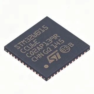
PN5190B1EV - 13.56MHz High-Power NFC Frontend IC | NXP
MPN: PN5190B1EV ✓ Active| Qty | Unit Price | Extended |
|---|---|---|
| 1 | $10.62 | $10.62 |
| 10 | $10.09 | $100.90 |
| 100 | $9.56 | $956.00 |
| 500 | $9.03 | $4,515.00 |
| 1,000 | $8.5 | $8,500.00 |
PN5190B1EV Overview
An NFC (Near Field Communication) frontend IC is the analog radio layer of a contactless system: it drives the antenna coil, demodulates the 13.56 MHz carrier, and implements the protocol stack interfaces, while a host microcontroller manages the application logic. Within the system hierarchy, the PN5190B1EV sits between the antenna-matching network and the host MCU, complementing secure elements and application processors in a complete NFC reader architecture.
Key features include multi-protocol support covering FeliCa, ISO 14443-A, ISO 14443-B, ISO 15693, ISO 18000-3, ISO 18092 (NFCIP-1), ISO 21481 and MIFARE, plus host interfaces of I2C, SPI and USB. The B1 silicon version, used with firmware V2.0 or higher, delivers the high RF output power required to energize cards at extended read ranges and to maintain reliable transactions with poorly coupled antennas - the defining trait of this high-power family.
Architecturally, the PN5190B1 integrates a low-jitter PLL, programmable power amplifier, adaptive receiver front end, and an embedded sequencer that offloads protocol timing from the host. The B1 silicon revision improves RF calibration and robustness versus the earlier A0 version (PN5190B0), and ordering-code suffixes select firmware/flash configurations.
Typical applications include POS payment terminals, contactless access control readers, vending machines, and industrial handhelds where dense metal environments, long cable runs to the antenna, or EMC stress degrade ordinary reader performance.
A key design consideration: this is a frontend, not a standalone reader - the host must run the PN5190 firmware stack via I2C/SPI, and the RF matching network must be tuned per the NXP antenna design-in package, which NXP supplies separately from the public datasheet.
This page synthesizes distributor pricing, same-package alternatives, and design guidance not consolidated in the manufacturer datasheet.
Drop-in alternatives for PN5190B1EV — same package, pin-to-pin compatible. Different-package parts requiring PCB rework are excluded.
Quick Comparison Tool — Select alternative parts for side-by-side comparison:
PN5190B1EV/C121E
✅ Drop-In📋 Reference alternative (not in catalog)
PN5190B1EV/C121Y
✅ Drop-In📋 Reference alternative (not in catalog)
PN5190B1EV/C127E
✅ Drop-In📋 Reference alternative (not in catalog)
PN5190B1EV/C127K
✅ Drop-In📋 Reference alternative (not in catalog)
PN5190B1EV/C127Y
✅ Drop-In📋 Reference alternative (not in catalog)
PN5190B0EV/C120Y
✅ Drop-In📋 Reference alternative (not in catalog)
PN5190B1EV Specifications
| Function | High-power NFC frontend IC (reader/writer, P2P, card emulation) |
| Carrier Frequency | 13.56 MHz |
| Supply Voltage | 2.4 V to 5.5 V |
| Protocols Supported | FeliCa, ISO 14443-A, ISO 14443-B, ISO 15693, ISO 18000-3, ISO 18092, ISO 21481, MIFARE |
| NFC Forum Compliance | NFC |
| Host Interfaces | I2C, SPI, USB |
| Package | 64-VFBGA |
| Mounting Type | Surface Mount |
| Silicon Version | B1 (with firmware V2.0 or higher) |
| Product Family | PN5190 NFC Frontend |
| Target Applications | Payment, physical access control, challenging RF environments |
| Output Power Class | High-power |
PN5190B1EV 64-vfbga Pin Configuration Guide
Pin configuration for PN5190B1EV (64-vfbga package). Pin numbering, functions, and connection diagrams are defined in the manufacturer datasheet. Refer to it for the exact footprint and soldering guidelines.

No detailed pinout data available for PN5190B1EV.
Refer to the datasheet for full pin configuration.
Typical Applications
PN5190B1EV is suitable for 6 applications: POS Payment Terminals, Physical Access Control Readers, Vending Machines and Kiosks, Industrial Handheld and Rugged Scanners, Transit Fare Collection, Embedded NFC Pairing Modules.
POS Payment Terminals
The PN5190B1EV is purpose-built for EMV contactless payment terminals, where NXP explicitly targets payment and challenging RF environments. Its high-power 13.56 MHz output sustains reliable transactions with cards presented at shallow angles or partially coupled to embedded antennas, while ISO 14443-A/B and FeliCa coverage satisfies global card schemes. In a typical terminal, the frontend sits between the antenna matching network and the secure-application MCU, connected via SPI for low-latency transaction handling. Unlike lower-power reader ICs, it maintains field strength under EMC stress from the terminal's own power and display circuitry, reducing transaction failure rates at the point of sale.
Recommended
Physical Access Control Readers
For door and gate access readers, the PN5190B1EV delivers the high RF power needed to read MIFARE and ISO 14443 credentials through metal housings, long antenna cable runs, and crowded mounting environments - the challenging RF conditions NXP cites for this part. Full ISO 15693 and ISO 18000-3 support extends coverage tovicinity cards and long-range badges beyond proximity-class ISO 14443. The frontend streams tag data to a host controller over I2C or SPI, while its adaptive receiver maintains decode margin near metal door frames. Designers should budget for the NXP antenna matching network and EMC layout package, since access-reader performance depends heavily on coil tuning rather than the IC alone.
Recommended
Vending Machines and Kiosks
Unattended vending and kiosk terminals embed NFC antennas behind metal fascias and face wide temperature and vibration stress, exactly the hostile RF coupling scenario the high-power PN5190B1EV was engineered for. Its 2.4V-5.5V supply integrates directly with existing kiosk rails, and USB connectivity simplifies interfacing with payment head modules already using USB. Multi-protocol support including ISO 18092 (NFCIP-1) enables peer-to-peer interactions for configuration and loyalty apps. Because transactions occur unattended, the frontend's robust field generation reduces retry loops that would otherwise cause customer-visible failures, and firmware updates on B1 silicon can be maintained over the same host link.
Recommended
Industrial Handheld and Rugged Scanners
Battery-powered industrial handhelds for asset tracking, logistics and maintenance benefit from the PN5190B1EV's combination of 2.4V minimum supply - allowing direct single-cell Li-ion operation - and high output power for reading tags at usable range. Protocol breadth spanning ISO 14443, ISO 15693 and ISO 18000-3 lets one device read asset tags, employee badges and transit credentials. The 64-VFBGA package keeps board area small inside handheld enclosures, while SPI offers the lowest-power host link. Designers should pair it with an efficient boost/buck stage and place the matching network close to the RF balls to minimize loss in compact antenna layouts.
Recommended
Transit Fare Collection
Transit gates and onboard validators must read diverse fare media - FeliCa in Japan, MIFARE and ISO 14443 in most other regions - and the PN5190B1EV covers all of these protocols in one IC, alongside ISO 18092 for NFC-phone wallet payments. Its high-power drive keeps read reliability high as passengers tap quickly at varied angles and distances, a critical throughput metric at fare gates. Host communication over I2C or SPI links the frontend to the gate controller, with USB available for maintenance interfaces. The high transaction rates and 24/7 duty cycle favor the B1 silicon revision's improved RF robustness versus the earlier A0 part.
Recommended
Embedded NFC Pairing Modules
Industrial IoT gateways and network equipment use NFC purely for commissioning - tapping a phone or badge to provision certificates, SSIDs and node identities. For this role the PN5190B1EV's card-emulation and peer-to-peer modes via ISO 18092, plus USB or I2C host links, make integration straightforward. The high-power frontend also tolerates mounting near metal enclosures common in industrial equipment, where a low-power reader would struggle. Because provisioning is bandwidth-light, the frontend can share an existing MCU and only be powered during provisioning events, keeping standby consumption negligible. Ensure the antenna region is kept clear of conductive enclosure features during mechanical design.
Recommended
Recommended Products Summary
Engineering reference data for PN5190B1EV — comparison, design guidance, and compliance information.
Selection Guide
Comparison with Alternatives
| Parameter | This Product | PN5190B1EV/C121E | PN5190B1EV/C127Y | PN5190B0EV/C120Y |
|---|---|---|---|---|
| Package | 64-VFBGA | 64-VFBGA - same | 64-VFBGA - same | 64-VFBGA - same |
| Brand | NXP Semiconductors | NXP Semiconductors | NXP Semiconductors | NXP Semiconductors |
| Silicon Revision | B1 | B1 | B1 | A0 |
| Firmware Requirement | V2.0 or higher | V2.0 or higher | V2.0 or higher | A0-generation firmware |
| Protocols | FeliCa, ISO 14443-A/B, ISO 15693, ISO 18000-3, ISO 18092, ISO 21481, MIFARE | Same protocol set | Same protocol set | Same protocol set |
| Host Interfaces | I2C, SPI, USB | I2C, SPI, USB | I2C, SPI, USB | I2C, SPI, USB |
Key Differentiators
- Latest B1 silicon revision (vs PN5190B0EV/C120Y)
- Multi-protocol breadth including FeliCa and ISO 18092 (vs PN5190B1EV/C127K (single-suffix variants share this))
- Three host interface options (vs PN5190B0EV/C120Y)
Design Notes
The PN5190B1EV requires a tuned 13.56 MHz matching network between the RF output balls and the antenna coil. NXP explicitly states that antenna design-in information is provided separately from the public PN5190B1 datasheet - request the NXP antenna design package and EMC application notes before finalizing layout. Keep RF traces symmetric and as short as possible; mismatches reduce read range disproportionately on this high-power part versus low-power reader ICs.
Operate from a clean 2.4V-5.5V rail with bulk and high-frequency decoupling close to the supply balls. As a high-power frontend, transmit-mode current draw peaks well above idle, so size the regulator for pulsed RF load transients and verify supply droop does not trigger brown-out during full-field operation. Estimated: budget for transmit current per the datasheet electrical specification tables before selecting the DC-DC stage.
The PN5190B1EV is a frontend only - it cannot function without a host MCU running the NXP PN5190 firmware stack, and B1 silicon requires firmware V2.0 or higher per the datasheet. Do not mix B1 hardware with A0-generation firmware binaries. Also verify the ordering-code suffix (C121E/C121Y/C127E/C127K/C127Y) matches your firmware provisioning flow and delivery requirement before ordering production quantities.
Compliance Information
Compliance data not present in the provided verified web data. Consult the NXP product page for PN5190B1EV for current RoHS/REACH declarations.