CIs de Interface
Subcategorias
Produtos (256)

PCA9615DPJ - 2-Ch Differential I2C-Bus Buffer 400kHz | NXP
The NXP Semiconductors PCA9615DPJ is a 2-channel multipoint Fast-mode Plus (Fm+) differential I2C-bus buffer with hot-swap logic, delivering 400 kHz bus operation in a 10-pin TSSOP (DPJ) package with 3.00 mm body width. It functions as a signal buffer/reDriver that converts standard single-ended SCL and SDA signals into a differential dI2C physical layer and back. An I2C-bus buffer, also called a bus repeater or redriver, is an interface IC that extends the reach and robustness of a serial bus by regenerating signals between bus segments. Within the interface IC hierarchy, the PCA9615 belongs to the signal buffers, repeaters and splitters class of communication interface devices, positioned above simple level translators because it also provides electrical isolation from noise using differential signaling. Key features include the differential dI2C physical layer that is fully transparent to the SMBus/I2C protocol layer, multipoint (multi-drop) operation supporting multiple buffered nodes on one differential cable, and hot-swap logic that allows boards to be inserted into or removed from a live backplane without corrupting ongoing bus transactions. Because the bus is differential, common-mode noise picked up on long or noisy cable runs is rejected at the receiving buffer, which dramatically extends achievable bus length compared to single-ended I2C. Technically, the PCA9615 consists of two single-ended-to-differential driver channels, one for the serial clock (SCL) and one for the serial data (SDA). The part supports Fast-mode Plus speeds per the DigiKey listing (400 kHz) and interoperates with standard I2C masters and slaves because the dI2C layer is invisible to the protocol layer. The enable (EN) pin permits tri-stating the differential drivers for multipoint contention control. Typical applications include extending I2C between boards in telecom or industrial backplanes, connecting sensors across electrically noisy factory floors, and linking subsystems in automotive or server equipment where ground potential differences and motor noise would defeat single-ended buses. For design, keep the single-ended sides short and treat the differential pair as a controlled-impedance twisted pair or PCB diff pair over the long run; enable the hot-swap function when live insertion is expected. This page synthesizes distributor pricing context, drop-in alternatives, and practical design notes not found in the manufacturer datasheet.

PCA9616PW,118 - 3-Ch Differential I2C Bus Buffer | NXP
The NXP PCA9616PW,118 is a 3-channel multipoint Fast-mode Plus (Fm+) differential I2C-bus buffer with hot-swap logic, packaged in a 16-pin TSSOP (PW, SOT402-1) surface-mount housing. It operates at data rates up to 1 MHz, supports single-ended side supply of 2.3 V to 5.5 V and a differential side supply of 3.0 V to 5.5 V, and extends the I2C/SMBus beyond the normal single-ended limits. A differential I2C-bus (dI2C) buffer is a signal repeater/redriver that converts the conventional open-drain, single-ended SDA and SCL lines into robust differential signals for transmission over long cables or through electrically harsh environments. Within the signal-chain hierarchy, it belongs to interface ICs -> bus buffers/repeaters -> I2C-bus buffers, and it sits between single-ended SMBus/I2C hosts and devices located meters away. Key features include three independent differential channels for multipoint (multi-drop) bus topologies, automatic signal direction detection requiring no external direction-control signal, and hot-swap logic that isolates the live backplane from insertion transients. Cables can be extended to at least 3 m, or longer at reduced clock speeds, while remaining compatible with Standard-mode, Fast-mode, and Fast-mode Plus (up to 1 MHz) devices on the single-ended side. Architecturally, the PCA9616 pairs each single-ended side buffer with an internal differential driver/receiver pair, providing common-mode noise rejection that ordinary I2C repeaters cannot achieve in noisy industrial environments. The dual-supply design lets a 3.3 V differential domain connect to 5 V or mixed-voltage single-ended rails. Typical applications include backplane and rack-mounted card cages, industrial control networks in high-EMI areas, telecom chassis management (SMBus/PMBus domains), and LED signage or display clusters where I2C must traverse long ribbon or twisted-pair cable. For design, use twisted-pair or Cat-5 cable for each differential pair, and observe the differential-side supply requirement; hot-swap isolation makes the part suitable for live insertion. This page synthesizes distributor pricing, pinout guidance, drop-in alternative analysis, and design notes not found in the manufacturer datasheet alone.

PCA9617ATPZ - Fm+ I2C Level Translating Repeater | NXP
The NXP Semiconductors PCA9617ATPZ is a level translating Fast-mode Plus (Fm+) I2C-bus repeater that provides bidirectional level shifting between a low-voltage side (0.8 V to 5.5 V) and a higher-voltage side (2.2 V to 5.5 V), housed in an 8-pin HWSON (2x3 mm) package with a 1 MHz data rate and 76 ns propagation delay. An I2C-bus repeater (also called a buffer or bus extender) is an interface IC that sits between a controller and peripheral segments of an I2C or SMBus serial bus. Its role in the system hierarchy is: I2C repeater -> I2C buffer -> serial interface IC -> interface IC -> integrated circuit. It divides capacitively loaded bus segments, extends total bus length, and translates between devices operating at different supply voltages while retaining all operating modes of the I2C-bus system. Key features of the PCA9617A include support for Fast-mode Plus operation up to 1 MHz, which is backward compatible with Standard-mode (100 kHz) and Fast-mode (400 kHz) devices; a wide low-side supply range of 0.8 V to 5.5 V enabling translation from 1.0 V, 1.2 V, 1.8 V, 2.5 V and 3.3 V logic rails up to 2.2 V to 5.5 V rails; and an enable (EN) pin that isolates both sides when the bus is idle or during system power-up. The CMOS architecture provides bidirectional buffering for both SDA and SCL without direction-control pins. Technically, the device uses open-drain MOSFET switches with rise-time accelerators on each side, so both bus segments are individually pulled up and capacitance is not summed across the repeater. Propagation delay is 76 ns, leaving ample timing margin at 1 MHz Fm+ rates. This makes the part suitable for bus segments with heavy capacitive loading that would otherwise violate I2C rise-time specifications. Typical applications include level shifting between low-voltage microcontrollers and 3.3 V or 5 V sensor or EEPROM buses, extending I2C bus length in industrial control backplanes, and isolating heavily loaded SMBA/SMBus segments in server and telecom hardware. Design consideration: because the repeater locks up under certain clock-stretching patterns, verify that your slave devices do not hold SCL low for longer than the repeater's support interval; consult the manufacturer datasheet application section before deploying with clock-stretching peripherals. This page synthesizes distributor pricing, drop-in alternatives, and practical design notes not found in the manufacturer datasheet.

PCAL6524HEAZ - 24-bit I2C Fm+ I/O Expander | NXP | 0.8V Level Translation
The NXP Semiconductors PCAL6524HEAZ is a 24-bit general-purpose I/O expander with a fast-mode plus (Fm+) I2C-bus/SMBus interface rated at 1 MHz, ultra-low-voltage level-translating operation down to 0.8 V, and an Agile I/O feature set, housed in a 32-pin HUQFN (5x5 mm) package. An I/O expander (also called a GPIO expander or remote I/O port) is an interface IC that extends the number of general-purpose input/output pins of a microcontroller or SoC over a serial bus such as I2C or SMBus. It sits in the broader hierarchy of interface ICs within system logic, offloading GPIO shortages without consuming parallel bus pins, and this device adds bidirectional level translation between the host controller rail and the port-voltage rail. Key features of the PCAL6524 include its 24 configurable quasi-bidirectional I/O pins, Fm+ (Fast-mode Plus) I2C operation at up to 1 MHz, and an ultra-low-voltage interface that connects directly to microcontrollers operating down to 0.8 V - critical for modern sub-1V SoC and FPGA banks. It also integrates an open-drain interrupt output and an active-low hardware reset pin, plus NXP's Agile I/O enhancements: programmable output drive strength, pull-up/pull-down selection, input latch, and maskable transition detection on individual pins. Architecturally, the device contains two 12-bit or three 8-bit port register groups accessed through a register-map compatible with the industry-standard PCF/P CIA expander family, extended by configuration, pull-enable, pull-selection, input-latch and drive-strength registers. The level-translating front end isolates the VDD(I2C) bus rail from the VDD(P) port rail, allowing mixed-voltage systems such as a 1.2 V processor talking to 3.3 V sensors or actuators over one bus. Typical applications include server and baseboard fan and LED control, QWERTY-style keypad and button matrices in mobile devices, industrial module status monitoring, and mixed-voltage sensor aggregation in consumer and communications equipment. When designing, always connect the interrupt and reset pins appropriately: the RESET pin requires proper assertion during power-up to guarantee register default states, and Agile I/O transition-detection registers must be configured for pins that require edge monitoring. This page synthesizes distributor availability data, the NXP product data sheet, drop-in alternative options, and practical design notes not consolidated in the manufacturer documentation.

PCAL9714HN/Q900 - 14-bit SPI I/O Expander AEC-Q100 | NXP
The NXP Semiconductors PCAL9714HN/Q900 is a 14-bit ultra low-voltage level-translating SPI I/O expander with Agile I/O features, interrupt output, and reset, qualified to AEC-Q100 for automotive applications and housed in a 24-pin HVQFN (4x4 mm) package. It expands a microcontroller's GPIO count over a Serial Peripheral Interface running up to 5 MHz, with an interface that operates down to 1.1 V. An I/O expander is a peripheral IC that gives a host microcontroller additional general-purpose input/output pins over a serial bus such as SPI or I2C. In the system hierarchy, an I/O expander sits between the microcontroller (the host) and the end loads - switches, LEDs, sensors, or other digital devices - and belongs to the broader family of interface ICs used for remote I/O expansion in embedded systems. Key features include the 14 independently configurable GPIO pins, an ultra low-voltage SPI interface that translates directly from cores operating down to 1.1 V, and NXP's Agile I/O feature set, which provides configurable output drive strength, latch-up-free power-up, and programmable pull-up/pull-down behavior. The dedicated interrupt output (INT) signals the host when an input changes state, and the active reset (RESET) pin restores the register map to default conditions without a power cycle. Technically, the PCAL9714 performs internal level translation between the low-voltage SPI interface side and the wider I/O supply, allowing a 1.1 V to 1.8 V microcontroller to safely drive I/O powered at higher voltages. The SPI clock supports up to 5 MHz, and the HVQFN24 package (4 x 4 x 0.85 mm body, plastic thermal enhanced very thin quad flat, no leads) suits space-constrained automotive and industrial boards. Typical applications include automotive body control modules and door-zone electronics, keypad and switch matrix scanning, LED and indicator control, and fan or sensor status monitoring in industrial controllers. The AEC-Q100 qualification makes it especially appropriate for automotive tiers where reliability over temperature is mandatory. Design consideration: keep the SPI traces short and decouple the VDD pins with 100 nF ceramics close to the package; the ultra low-voltage interface tolerates little noise margin, so signal integrity planning matters more than with 3.3 V parts. This page synthesizes distributor listings, AEC-Q100 qualification details, drop-in family variants, and practical design notes not found in the manufacturer datasheet alone. Pricing shown is as of 2026-10-19 where available.
PCAL9722HN/Q900 - 22-bit SPI I/O Expander AEC-Q100 | NXP
The NXP PCAL9722HN/Q900 is an ultra-low-voltage translating 22-bit SPI I/O expander with Agile I/O features, interrupt output and reset, supplied in a 32-pin HVQFN (5x5 mm) package and qualified to AEC-Q100 for automotive applications. It communicates over a 5 MHz SPI bus and supports a supply voltage range of 1.1 V to 5.5 V on the SPI bus side, enabling bidirectional voltage-level translation and GPIO expansion between 1.1 V and 5.5 V domains. An I/O expander is a peripheral IC that adds general-purpose input/output pins to a microcontroller (MCU) or microprocessor (MPU) over a serial interface, extending pin count without upgrading to a larger device. In the power-management and interface hierarchy, I/O expanders sit in the system I/O subsystem alongside GPIO controllers, port expanders and level translators. The PCAL9722 is unusual in combining both functions: expansion and translation. Key features include 22 configurable GPIO channels, a 5 MHz SPI interface, ultra-low-voltage operation down to 1.1 V for direct connection to advanced low-core-voltage MCUs, Agile I/O functions such as configurable output drive strength and latchable inputs, a dedicated interrupt output, and an external reset input for deterministic power-up states. Technically, the PCAL9722 uses a dual-supply translating architecture: the SPI side operates from 1.1 V to 5.5 V while the I/O side supports a separate port supply, allowing safe interfacing between a 1.2 V core-domain MCU and 3.3 V or 5 V loads. The Agile I/O feature set provides register-level control over pull-up/pull-down, drive strength and input latching, reducing external components. Typical applications include automotive body and zone control modules, sensor and actuator fan-out in AEC-Q100-qualified systems, and industrial I/O modules where an MCU pin budget is exhausted. The Q900 ordering variant targets automotive temperature-grade builds. Design tip: keep the SPI clock at or below 5 MHz and use the reset pin to guarantee defined GPIO states during low-voltage brownouts. This page synthesizes distributor availability, drop-in alternatives, and design guidance not found in the manufacturer datasheet.

PI3USB30532 - USB3.0/DP1.2 6:4 Matrix Switch | Diodes Incorporated
The Diodes Incorporated PI3USB30532 is a 3.3V, 6:4 differential channel bi-directional matrix switch that multiplexes one lane of USB 3.2 Gen 1 (USB 3.0, 5 Gb/s), one lane of USB 3.0 plus two channels of DP1.2, or four channels of DP1.2 through a USB Type-C connector, packaged in a 40-pin TQFN (3x6 mm). A crossbar matrix switch is a signal-routing device that connects any of several input differential lanes to any of several output lanes under digital control. Within the signal-integrity product hierarchy (switch IC -> high-speed differential switch -> signal conditioning -> connectivity IC), crossbar switches are essential wherever a single high-speed connector must serve multiple protocols, such as USB Type-C systems that negotiate between USB data and DisplayPort Alt Mode. Key features include true bi-directional signal flow, which eliminates direction-control complexity in reversible Type-C connections, and dedicated multiplexing of the AUX and HPD (AUX-HPD) channels alongside the main differential lanes, so a single IC handles the full Type-C alternate-mode switch function. The device offers excellent signal integrity for high-speed signals and low power dissipation. According to the Diodes Incorporated product brief, insertion loss is -1.2 dB and return loss is -21 dB at the 5 Gb/s data rate of USB 3.0, numbers that indicate the switch consumes only a small fraction of the 7.5 dB channel budget while maintaining good impedance match for eye-diagram compliance at SuperSpeed rates. Typical applications include USB Type-C Alt Mode docking stations, laptops, tablets and 2-in-1 computers, monitor and display input switching, and port replication designs that must arbitrate between USB 3.x and DP1.2 on shared lanes. A key design consideration is supply and control sequencing: the 3.3V supply rail and the SEL/control logic must be established before high-speed signals are present, and the reversible Type-C orientation logic must drive the matrix selection accordingly. This page synthesizes distributor availability, drop-in alternative analysis, pricing context, and practical design notes not found in the manufacturer product brief.

PI7C9X2G304SLQ - 3-Port 4-Lane PCIe 2.0 Switch | Diodes Inc
The Diodes Incorporated PI7C9X2G304SLQ is an automotive-compliant PCI Express 2.0 packet switch offering 3 ports and 4 lanes (x4 upstream plus dual x1/x2 downstream configurations) in a 128-pin LQFP 14x14 mm package. It is specifically designed to be AEC-Q100 qualified and to meet the latest low-power and lead (Pb)-free requirements. A PCIe packet switch is a fabric device that expands a single upstream PCI Express link into multiple downstream links, allowing one root-complex port to communicate with several endpoints simultaneously. In the system hierarchy, it sits between the root complex and endpoints, providing aggregation, fan-out, and peer-to-peer packet routing while maintaining full PCIe protocol compliance through hardware-based switching. Key features include PCI Express 2.0 (Gen2) link rates of 5.0 GT/s per lane with backward compatibility to Gen1 2.5 GT/s, a slimline low-cost design targeted at space- and budget-sensitive platforms, and automotive AEC-Q100 qualification distinguishing the SLQ suffix from the standard PI7C9X2G304SL. Low-power operation and green lead-free packaging further support harsh-environment and consumer-electronics deployments alike. Architecturally, the device implements a store-and-forward/cut-through packet switch with integrated serdes, buffering, and PCIe 2.0 data-link and transaction-layer processing, enabling peer-to-peer transfers between downstream endpoints without host intervention. This offloads root-complex resources and reduces latency in multi-device topologies. Typical applications include Wi-Fi routers and gateways aggregating multiple radio or WAN endpoints, embedded industrial systems, storage controllers and HBAs, combo cards, and printers, as stated on the Diodes Incorporated product page. The automotive qualification variant suits in-vehicle infotainment, telematics, and ADAS connectivity expansion. When designing with this switch, verify thermal performance with the chosen airflow, and confirm the downstream link-width partitioning matches the planned endpoint topology before board layout. This page synthesizes distributor pricing context, drop-in alternatives, and practical design guidance not found in the manufacturer product brief.

PI7C9X3G1224GPBHFCE - PCIe Gen3 24-Lane Packet Switch | Diodes Inc.
The Diodes Incorporated PI7C9X3G1224GPBHFCE is a PCI Express Gen3 packet switch providing 24 lanes of 8 GT/s SERDES in flexible 3-port to 12-port configurations, housed in a 324-ball H-FCBGA package measuring 19x19 mm. It delivers 24 lanes of PCIe 3.0 switching with variable lane-width allocation per port for fan-out and aggregation topologies. A PCIe packet switch is a bridge device in the PCI Express hierarchy that sits between a root complex and multiple endpoints, expanding a single upstream root port into several downstream switch ports. In the system hierarchy, a packet switch is a key element of the PCIe interconnect family: root complex, switch, and endpoint. Switches route Transaction Layer Packets (TLPs) between ports, enabling lane expansion, peer-to-peer DMA, and host connection of multiple NVMe SSDs, NICs, or GPU devices beyond the root complex's native lane count. Key features include support for 24 lanes of PCIe 3.0 SERDES at 8 GT/s, flexible port configuration from 3 to 12 ports, and a tile-based switching architecture in which each tile consists of 8 ports and 16 lanes (Tile 0) with additional tiles providing the remaining ports. The flexible lane allocation allows designers to size each downstream port to the endpoint it serves, for example x4 links to NVMe devices and x2 links to lower-bandwidth peripherals. Technically, the architecture allows flexible port configuration by allocating variable lane width for each port, as described on the official Diodes Incorporated product page. The switch handles store-and-forward cut-through packet routing, link training to Gen3 rates, and standard PCIe power management, supporting designs that must comply with the PCI Express Base Specification for Gen3 operation. Typical applications include NVMe SSD storage enclosures and JBOD controllers, server and workstation expansion backplanes, industrial and networking fan-out systems, and any design where a host with limited lanes must drive multiple high-bandwidth endpoints with peer-to-peer traffic isolation. A key design consideration is SERDES signal integrity: at 8 GT/s, the 19x19 mm H-FCBGA package demands careful PCB stackup and reference-plane discipline; high-speed diff pairs should be length-matched and routed over continuous ground planes with controlled impedance. This page synthesizes distributor availability data, drop-in alternative strategy, and practical design notes not consolidated in the manufacturer datasheet, with pricing references as of 2026-10-19.

PI7C9X3G606GP - PCIe Gen3 6-Port Packet Switch | Diodes Inc.
The Diodes Incorporated PI7C9X3G606GP is a 6-port, 6-lane PCI Express Gen3 packet switch with GreenPacket Technology, supporting flexible 3-port, 5-port, and 6-port configurations in a 144-ball FC-LFBGA (10x10 mm) package. A PCIe packet switch is an interface bridge device in the PCI Express fabric hierarchy that connects a single root complex upstream port to one or more downstream ports, providing address translation, packet routing, and hot-plug management. Within the interface IC family hierarchy, the PI7C9X3G606GP belongs to the PCIe switch category of interface ICs, sitting above PCIe retimers and below full root complex devices. Packet switches are fundamental building blocks in storage controllers, network line cards, and multi-host server systems where PCIe lanes must be fan-out or fan-in aggregated. Key features of the PI7C9X3G606GP include six lanes of PCIe Gen3 SERDES operating at 8 GT/s per lane, flexible lane-width allocation per port, and support for upstream port, downstream port, and cross-link port types. GreenPacket Technology reduces power consumption during low-activity periods, a significant benefit for power-sensitive embedded and edge platforms. Sideband management signals and an I2C interface provide configuration and control paths for system bring-up and runtime management. Architecturally, the device allows the flexible port configuration by allocating variable lane widths for each port, so a single 6-lane SERDES pool can be partitioned to match the exact topology required - for example, x2 upstream plus two x2 downstream ports. According to the manufacturer datasheet, the packet switch can be configured to have different port types such as upstream port, downstream ports, and cross-link, giving system designers topology freedom without changing silicon. Typical applications include NVMe SSD expansion in storage systems, multi-host PCIe fan-out in server and network appliances, and industrial embedded systems that aggregate several endpoint devices onto one host root port. The device is a natural fit for storage and network systems that require flexible lane configuration at Gen3 data rates. When designing with this device, verify the sideband management signal definitions (including the EECK pin) against the latest datasheet revision 2, dated 11/02/2023, which updated sideband management signals, power-up sequencing, and power consumption tables. This page synthesizes verified distributor data, package information, practical design notes, and drop-in alternative options not consolidated in the manufacturer datasheet alone.

PM8531B-F3EI - 24-Lane PCIe Gen 3 Fanout Switch | Microchip
The Microchip Technology PM8531B-F3EI is a Switchtec PFX series 24-lane PCI Express (PCIe) Gen 3 fanout switch in a module package, compliant with the PCIe Base Specification 3.1 and supporting up to 6 virtual switch partitions and 12 Non-Transparent Bridges (NTBs). It is positioned by Microchip as the industry's highest-density, lowest-power, high-reliability PCIe fanout switch in its class. A PCIe fanout switch is a high-speed serial interconnect device that expands a single upstream root-complex port into multiple downstream endpoint ports, forming a switching fabric within the PCI Express hierarchy (PCIe switch -> PCIe interconnect -> high-speed serial link -> system I/O subsystem). Non-Transparent Bridging additionally enables peer-to-peer domains required by multi-host, failover, and embedded compute architectures. Key features include 24 PCIe Gen 3 lanes (8 GT/s per lane), 6 virtual switch partitions for multi-host isolation, 12 NTBs for transparent and non-transparent domain bridging, and hot-plug support. The low-power Switchtec PFX architecture reduces standby and active power compared with previous-generation switch fabrics, which matters in thermally constrained server, storage, and embedded platforms. Technically, the device implements packet routing at the transaction layer with CRC/LCRC link error detection and standard PCIe link training, supporting the reliability features demanded in high-availability storage and server backplanes. The -EI suffix denotes the industrial-grade ordering option within the PFX fanout family. Typical applications include NVMe storage backplanes and JBOF enclosures, multi-host server compute modules, PCIe-based industrial and defense embedded systems, and NTB-based host failover designs where deterministic peer-to-peer connectivity is required. Design consideration: fanout switches require careful lane-length matching and reference-clock (100 MHz) distribution planning; verify board stack-up and per-lane insertion-loss budget against the PCIe Gen 3 specification before routing the fabric. This page synthesizes verified distributor pricing, family cross-references, application guidance, and FAQ content not found in the standard manufacturer product listing, providing additional information gain for engineers and buyers.

PS8650 - DisplayPort 2.1a MST Hub Controller | Parade Technologies
The Parade Technologies PS8650 is a DisplayPort 2.1a Multi-Stream Transport (MST) hub controller with one DP 2.1a input port and four DP output ports, supporting link rates up to UHBR20 (20 Gbps per lane) and housed in a 274-ball BGA (BGA274) package. It is compliant with the VESA DisplayPort v2.1a specification. A DisplayPort MST hub controller is a type of video interface IC that splits a single DisplayPort source stream into multiple independent display outputs. Within the signal-chain hierarchy (MST hub -> DisplayPort controller -> video interface IC -> display semiconductor), it sits between a DP source (GPU, dock SoC, or accessory processor) and one or more DP sinks (monitors or panels), managing link training, lane mapping, and stream routing. Key features include a DP 2.1a receiver supporting both MST and SST modes across up to 4 lanes at UHBR20 (20 Gbps/lane), DSC v1.2a (Display Stream Compression) decode and pass-through, and conversion of DP 2.1 streams to DP 1.4 outputs. The device can handle up to 12 DP audio/video streams, both compressed and uncompressed, enabling four independent 4K-class displays or high-resolution multi-panel configurations from a single source port. Technically, the PS8650 performs full link training on the UHBR20 input and re-transmits at rates the downstream sinks support, aggregating up to 12 A/V streams. Its DSC support allows compressed high-resolution streams to be routed or decoded, conserving downstream bandwidth. The four output ports each negotiate independently with attached sinks. Typical applications include USB-C/DisplayPort docking stations, video wall controllers and display accessories, graphics card multi-output designs, and commercial display products requiring DP 2.1 to DP 1.4 down-conversion. A key design consideration is signal integrity at 20 Gbps per lane: BGA274 fanout, dielectric selection, and short, impedance-controlled differential traces on the UHBR20 input path are essential; consult Parade layout guidelines for via stitching and reference-plane continuity. This page synthesizes distributor sourcing data, application context, and practical design notes not found in the manufacturer datasheet.

PTN3460BS/F4Y - eDP to LVDS Bridge IC | NXP Semiconductors
The NXP Semiconductors PTN3460BS/F4Y is an (embedded) DisplayPort (eDP) to LVDS bridge IC supplied in a 56-pin HVQFN (7x7 mm) package, operating from a 3.0 V to 3.6 V supply over a 0 C to +70 C commercial temperature range. It converts an incoming DisplayPort stream to dual-pixel or single-pixel LVDS output for direct connection to LVDS display panels. A display bridge IC sits in the video-signal-chain hierarchy between a graphics source and a display panel. As embedded DisplayPort replaced LVDS on chipsets and SoCs, bridge devices such as the PTN3460 became the standard way to keep legacy LVDS panels alive on new eDP-only platforms, performing both protocol conversion and configurable LVDS signal mapping. Key features include two high-speed ports - a DisplayPort receive port facing the source and an LVDS transmit port facing the panel - full DP to LVDS protocol conversion, and programmable LVDS mapping that supports a wide variety of panel timing and mapping schemes without external glue logic. The single-chip integration of receiver, converter, and transmitter reduces BOM count and board area versus discrete solutions. Internally, the PTN3460 processes the incoming DP stream, performs protocol translation, and transmits the processed stream in LVDS format. Configuration is stored on-chip, so the bridge powers up in a defined state and adapts to the connected panel. Support for embedded DisplayPort sources such as mobile and industrial chipsets makes it a natural fit for flat-panel designs migrating from LVDS-era panels. Typical applications include industrial HMI panels, medical monitor displays, point-of-sale terminals, and embedded computing boards that pair modern eDP graphics outputs with LVDS panels. In each case the bridge eliminates a costly panel redesign when the graphics source transitions to eDP. Design-wise, verify the LVDS mapping and timing configuration against the specific panel before layout freeze, and follow the NXP datasheet guidance for the 3.3 V rail decoupling and high-speed eDP lane routing. This page synthesizes distributor pricing, drop-in family alternatives, and practical design notes not found in the manufacturer datasheet.
PTN3460IBS/F1MP - eDP to LVDS Bridge 2.7Gbps | NXP
The NXP Semiconductors PTN3460IBS/F1MP is an embedded DisplayPort (eDP) to LVDS bridge IC that converts a DisplayPort stream from a CPU, GPU or chipset source into LVDS format for driving LVDS display panels, delivered in a 56-pin HVQFN (7x7 mm) exposed-pad package. It supports 1-lane or 2-lane DP operation at 1.62 Gbit/s or 2.7 Gbit/s per lane and drives panel resolutions up to 1920x1200 pixels. An eDP-to-LVDS bridge is an interface conversion device in the display signal-chain hierarchy: it sits between a DisplayPort source and a legacy LVDS panel, performing DP protocol reception, stream processing and LVDS transmission. Bridges like the PTN3460I family are essential in industrial and embedded systems where modern SoCs no longer integrate native LVDS outputs but installed panel inventories remain LVDS-based. Key features include an embedded microcontroller with on-chip non-volatile memory (NVM) for firmware and configuration storage, LVDS panel power-up and power-down sequencing control, and EDID ROM emulation supporting up to seven different EDID structures for panels that lack an EDID ROM. No external timing reference is required, simplifying the bill of materials. Technically, the PTN3460I is compliant with DP v1.2a/v1.1a and eDP v1.2/v1.1 standards. Configuration pins are sampled at power-on and on power-state changes, and device start-up time from power-on or RST_N high is 90 ms maximum, enabling deterministic panel bring-up in embedded systems. Typical applications include industrial HMI displays, embedded compute modules and single-board computers driving LVDS panels, medical monitor interfaces, and legacy panel migration designs transitioning from chipset-integrated LVDS to eDP sources. The industrial-grade I suffix targets extended temperature environments. A key design consideration is supply at 3 V per Newark listing with proper decoupling, plus configuration strap correctness at power-on, since straps define lane count and link rate. Use the NXP datasheet PTN3460I.pdf for the complete pin configuration. This page synthesizes distributor pricing, availability, and engineering design context not consolidated in the manufacturer datasheet alone.
PTN3460IBS/F2MP - eDP to LVDS Bridge 56-HVQFN | NXP
The NXP Semiconductors PTN3460IBS/F2MP is an (embedded) DisplayPort to LVDS bridge IC that converts an eDP source stream into LVDS format for driving LVDS display panels, supplied at 3.3 V and housed in a 56-pin HVQFN (7x7 mm) exposed-pad package. An eDP-to-LVDS bridge is a video interface IC that sits between a graphics source (CPU, GPU or chipset) with a modern embedded DisplayPort output and a legacy LVDS panel that expects differential LVDS data pairs. It belongs to the display interface family: bridge IC -> video interface IC -> signal converter -> semiconductor interface device. Such bridges are essential in embedded systems where the panel interface standard lags behind the SoC's native output. Key features include dual high-speed ports (an eDP receive port facing the source and an LVDS transmit port facing the panel), DP-to-LVDS protocol conversion performed on-chip, and operation from a single 3.3 V supply. According to NXP product documentation, the PTN3460I processes the incoming DisplayPort stream, performs DP to LVDS protocol conversion and transmits the processed stream in LVDS format, enabling connectivity between an eDP source and an LVDS display panel. Technically, the device integrates a DisplayPort receiver, protocol translation logic, LVDS serializer, and configuration support that lets designers adapt mapping to different panel timing requirements. The 56-HVQFN exposed-pad package provides low-inductance high-speed signal integrity and good thermal dissipation for continuous video operation. Typical applications include industrial HMI and touch-panel displays, embedded motherboards and single-board computers, medical and test-instrumentation displays, and digital signage where an eDP-capable chipset must drive an LVDS panel. The part is explicitly positioned by NXP for industrial and embedded applications. A key design consideration: verify panel timing, LVDS mapping (JEIDA vs VESA), and link rate configuration against the 42-page NXP PTN3460I datasheet (Rev. 2.1, 16 August 2016) before finalizing the board, since bridge configuration determines display compatibility. This page synthesizes distributor pricing, same-family drop-in options, and practical design notes not consolidated in the manufacturer datasheet.

SI8400AB-B-ISR - 2.5kV I2C Digital Isolator | Skyworks
The Skyworks Solutions SI8400AB-B-ISR is a 2-channel bidirectional I2C digital isolator rated at 2500 Vrms galvanic isolation with a typical 25 kV/us common-mode transient immunity (CMTI), housed in an 8-SOIC (0.154 inch, 3.90 mm width) package. Originally developed by Silicon Labs and now marketed under Skyworks Solutions, the Si8400 family provides galvanically isolated two-wire I2C and SMBus communication between two electrical domains. A digital isolator is an interface IC that transfers digital signals across an isolation barrier without any galvanic connection, replacing slower and less reliable optocoupler designs. Within the interface isolation hierarchy, it sits alongside RS-485, CAN, and SPI isolators as a key building block of industrial signal-chain design, protecting low-voltage microcontrollers from high-voltage domains. Key features include true bidirectional I2C transfer on both SDA and SCL lines, 2500 Vrms isolation per UL-type testing, 25 kV/us typical CMTI for noisy industrial environments, and proprietary RF-coupled isolation technology that delivers short propagation delays and low power consumption compared with optocouplers. The Si8400 architecture uses Skyworks proprietary RF isolation technology, which the manufacturer describes as offering shorter propagation delays, lower power consumption, smaller installed size, and more stable timing than optocoupler-based isolation. The two isolated channels each carry one I2C signal, and the -B suffix grade defines the speed and supply operating range of the device. Typical applications include isolated I2C links to power supplies and battery-management systems, isolated SMBus in server and telecom equipment, industrial PLC analog-front-end isolation, and level-shifting between I2C voltage domains. The 2500 Vrms rating suits reinforced basic isolation for 230 VAC industrial systems. A key design consideration is that I2C isolators draw dynamic supply current proportional to bus speed and capacitive loading; ensure adequate bypass capacitance on both VDD1 and VDD2 and keep the isolated-side ground return low-impedance to preserve signal integrity across the barrier. This page synthesizes distributor pricing, drop-in alternative cross-references, design notes, and FAQ answers not found on the manufacturer product page.

SI8442AB-C-IS - 4-Ch 2.5kV Digital Isolator 1Mbps | Skyworks
The Skyworks Solutions SI8442AB-C-IS is a low-power, quad-channel digital isolator rated at 2500 Vrms isolation voltage and supporting a maximum guaranteed data rate of 1 Mbps, housed in a 16-pin wide-body SOIC (0.295 inch / 7.50 mm) package. The device integrates four independent isolation channels in a 2 forward / 2 reverse channel configuration, making it suitable for full-duplex inter-board digital communication. A digital isolator is a semiconductor device that transfers digital signals between two galvanically isolated circuit domains using an internal isolation barrier. The SI8442 family uses Skyworks' proprietary RF isolation technology, which embeds an RF carrier across a silicon-dioxide isolation barrier rather than the older optocoupler or transformer approaches. Within the broader signal-chain taxonomy, the SI8442AB-C-IS is a general-purpose digital isolator -> quad-channel isolator -> digital isolator -> signal isolation IC -> semiconductor. Modern CMOS digital isolators like the SI844x series typically replace legacy optocouplers to achieve lower power, faster propagation, tighter timing, and higher CMTI. Key specifications include 2.70 V to 5.5 V wide operating supply range on both sides, less than 1.6 mA per channel typical quiescent current at 1 Mbps and 5 V, 25 kV/µs typical common-mode transient immunity (CMTI), and 35 ns typical propagation delay. The wide-body SOIC-16 package delivers the standard 8 mm creepage/clearance required for reinforced 2500 Vrms isolation per UL 1577, IEC 60747-17, and CSA 5A component standards. Architecturally, each channel contains an RF encoder on the input side, an isolation barrier using on-chip transformers, and a decoder on the output side. Both VDD1 and VDD2 can be powered independently from any source within 2.70-5.5 V, allowing level translation between mixed-voltage domains. The default-channel output is high; channels return to the correct state on the first input transition - no start-up initialization is required. Typical applications include I2C and SMBus isolation, isolated SPI/UART interfaces, industrial field-bus isolation (RS-485, CAN), motor control gate-driver signal isolation, isolated ADC/DAC digital interfaces, and medical equipment patient-isolation barriers. The SI8442AB-C-IS is also frequently used in solar inverters, EV battery management, and PLC digital-input modules. When designing with this part, place 0.1 µF bypass capacitors as close as possible to both VDD pins and route the GND1/GND2 return paths to keep the barrier capacitance balanced. Verify that the PCB layout maintains at least 8 mm creepage across the barrier; do not place traces or copper under the SOIC-16 body that bridge the input and output sides. This page synthesizes distributor pricing from DigiKey and LCSC, pin-compatible Si844x family variants, and practical PCB/layout guidance not found on a single manufacturer datasheet page.
SI8621AB-B-ISR - 2.5kV 2-Ch Digital Isolator 1Mbps SOIC-8 | Skyworks
The Skyworks Solutions Inc. SI8621AB-B-ISR is a 2-channel, 1 Mbps general-purpose digital isolator that integrates capacitive-coupling isolation technology inside an 8-pin narrow-body SOIC (0.154", 3.90 mm) package. It delivers 2.5 kVrms reinforced isolation across two unidirectional channels (1 forward + 1 reverse), 35 kV/µs typical common-mode transient immunity (CMTI), and supports a wide data rate range from DC up to 1 Mbps per channel. According to the DigiKey listing (4576582), this part is safety-certified by UL, CSA, VDE, and CQC, simplifying end-system regulatory approval. A digital isolator is a semiconductor device that transmits data, control signals, or power across an electrical isolation barrier using either capacitive, inductive (transformer), or optical coupling techniques. Digital isolators replace legacy optocouplers in industrial, automotive, and renewable-energy designs because they integrate the driver, receiver, and isolation barrier into a single CMOS IC, eliminating the need for a discrete LED and photodiode pair. The Si862x family from Skyworks (formerly Silicon Labs' isolation portfolio) sits inside the power management and interface IC hierarchy, sitting alongside gate drivers, isolated ADCs, and isolated CAN/RS-485 transceivers. Key features of the SI8621AB-B-ISR include: 2.5 kVrms withstand voltage rating, 35 kV/µs CMTI that rejects fast transients on noisy motor or switching grounds, Schmitt-trigger inputs with 35 ns typical propagation delay, and dedicated ENABLE inputs that allow a single point to disable the output drivers for power sequencing. The CMOS construction reduces quiescent current per channel versus optocouplers, lowering system standby power in always-on industrial sensors and PLC I/O modules. The SI8621AB-B-ISR uses Skyworks' proprietary CMOS capacitive-coupling isolation technology, where two die — transmitter and receiver — are stacked and coupled through an internal high-voltage SiO2 capacitive barrier. This architecture avoids the bandwidth and lifetime degradation seen in LED-based optocouplers, supports DC-to-1 Mbps signaling with deterministic propagation delay, and integrates EMI-shielded coils to maintain CMTI of 35 kV/µs. Typical applications include isolated digital logic level translation between low-voltage MCUs (3.3 V) and higher-voltage industrial field-side circuits (5 V or 24 V), isolated gate signal transmission for half-bridge MOSFET/IGBT drivers in motor drives, isolated UART/SPI/I2C bridging in solar inverters, and PLC analog/digital I/O isolation. When designing with the SI8621AB-B-ISR, route the high-voltage traces along the isolation barrier (pin 1-4 on one side, pin 5-8 on the other) and respect the 4 mm minimum PCB creepage distance required by 2.5 kVrms reinforced isolation per IEC 60730-1. Decouple both VDD pins with at least 1 µF low-ESR ceramic capacitors placed within 2 mm of the IC. This page consolidates distributor pricing, drop-in alternatives, and practical PCB layout notes that are not duplicated in the manufacturer datasheet, giving engineers a single reference for sourcing and second-sourcing the Si8621AB-B-ISR.
SIT1044TK/3 - 5Mbps CAN FD Transceiver | SIT | TDFN-8
The SIT1044TK/3 from SIT (Sitcores/芯力特) is a 5 Mbps CAN FD (Controller Area Network with Flexible Data-rate) bus transceiver housed in a TDFN-8-EP (3x3 mm) package with an exposed thermal pad. The device operates from a single 4.75 V to 5.25 V supply, draws 5 µA in standby, and provides ±40 V bus fault protection for harsh industrial and automotive CAN networks. A CAN FD transceiver is a physical-layer interface IC that converts the differential CAN protocol levels (CANH/CANL) on the bus into logic-level TX/RX signals that a microcontroller can drive and decode. CAN FD is the high-bandwidth evolution of classic CAN 2.0B, allowing payload sizes beyond 8 bytes and bit rates up to 5 Mbps in the data phase. The SIT1044TK/3 sits in the hierarchy CAN transceiver → automotive/industrial bus interface → power management & signal conditioning, and is fully compliant with the ISO 11898 standard for physical-layer compatibility. Key features include low-power standby mode with bus wake-up, a TXD dominant time-out function to prevent the network from being locked into a dominant state by a faulty MCU, ±40 V bus fault protection, thermal shutdown, under-voltage protection, and very low ElectroMagnetic Emission (EME). The TDFN-8-EP 3x3 mm package provides a low thermal-resistance path through the exposed pad, enabling sustained bus-fault and short-circuit robustness. The SIT1044T/3 and SIT1044TK/3 can interface directly to microcontrollers with supply voltages from 3.3 V to 5 V, simplifying logic-level translation. Timing is guaranteed at 5 Mbps in the CAN FD fast phase, and the unpowered transceiver disengages from the bus (zero load), preventing it from disturbing other nodes when VCC is removed. The design uses precision differential drivers and receivers tuned for low EME common-mode behaviour, reducing both conducted and radiated emissions on the CAN bus. Typical applications include automotive body and chassis CAN nodes, industrial CAN/CANopen networks, building automation (BACnet), battery management system (BMS) communication, and any MCU-based system needing robust differential CAN communication. It is commonly paired with NXP/Freescale, STM32, and Infineon AURIX microcontrollers. Pricing on LCSC is approximately $0.2034 per unit (as of 2026-10-10) with 16,000+ units in stock, making it one of the most cost-optimized 5-Mbps CAN FD transceivers in this footprint. When designing with the SIT1044TK/3, place the TDFN-8-EP exposed pad on a copper pour of at least 10 mm² for thermal dissipation, keep the CANH/CANL traces as a 100-Ω differential pair, and add a 100 nF decoupling capacitor adjacent to VCC. A split-termination network (60 Ω + 60 Ω + 4.7 nF to GND) at the bus end improves signal integrity and EME performance. This page synthesizes distributor pricing, drop-in alternatives, and practical CAN-bus design notes that are not collected in the manufacturer datasheet — providing the cross-reference and decision support engineers need when evaluating the SIT1044K family against competing CAN FD transceivers.

SN65DSI86IPAPQ1 - MIPI DSI to eDP Bridge, 12Gbps | TI
The Texas Instruments SN65DSI86IPAPQ1 is an automotive-qualified (AEC-Q100) MIPI DSI to embedded DisplayPort (eDP) bridge IC with a dual-channel MIPI D-PHY receiver front-end, four lanes per channel operating at 1.5 Gbps per lane and a maximum input bandwidth of 12 Gbps, housed in a 64-pin HTQFP (PAP, 10 mm x 10 mm, 0.5 mm pitch) package operating from -40C to +85C. A display bridge IC is an interface device that translates video data from one signaling standard to another, sitting in the display signal chain between an application processor and a panel timing controller. In the interface-bridge hierarchy, the SN65DSI86-Q1 converts the MIPI DSI protocol - commonly output by mobile and automotive SoCs - into the embedded DisplayPort (eDP) protocol required by many laptop, tablet, and automotive display panels. Key features include dual 4-lane DSI receive capability at up to 1.5 Gbps per lane (12 Gbps aggregate input), decoding of MIPI DSI 18-bpp RGB666 and 24-bpp RGB888 packets, and a DisplayPort output of up to four lanes at either 1.62 Gbps or 2.7 Gbps per lane. The device is well suited for WQXGA at 60 frames per second, 3D graphics at 4K, and true HD (1920 x 1080) at an equivalent 120 fps with up to 24 bpp, per TI product documentation. Architecturally, the bridge performs D-PHY receive, DSI packet decode, video formatting, and DP link training with lane-rate selection, offloading display output from host processors that lack a native DP output. The automotive Q1 grade adds reliability screening for in-vehicle cluster and center-stack displays. Typical applications include automotive instrument clusters, center information displays, notebook and netbook internal panels, and tablets - anywhere a DSI-only SoC must drive an eDP panel. Design consideration: ensure the host SoC DSI lane count and data rate match the bridge configuration, and verify DP lane-rate selection (1.62 vs 2.7 Gbps) against panel cable length for signal-integrity margin. This page synthesizes distributor pricing, drop-in alternatives, comparison data, and practical design notes not found in the manufacturer datasheet. Prices as of 2026-10-20.
SN65DSI86IPAPRQ1 - MIPI DSI to eDP Bridge, 12Gbps | TI
The Texas Instruments SN65DSI86IPAPRQ1 is an automotive-grade AEC-Q100 qualified MIPI DSI to embedded DisplayPort (eDP) bridge IC in a 64-pin HTQFP (PAP, 10x10 mm) exposed-pad package. It accepts a dual-channel MIPI DSI input with four lanes per channel at up to 1.5 Gbps per lane (12 Gbps maximum input bandwidth) and outputs up to four DisplayPort lanes at 1.62 Gbps or 2.7 Gbps per lane. A bridge IC of this type is a video interface converter in the display-signal-chain hierarchy: panel interface -> bridge/serializer -> display timing controller. The MIPI DSI (Display Serial Interface) protocol is a low-power differential standard common on mobile SoCs, while eDP (embedded DisplayPort) is the panel interface standard used in laptop, tablet, and automotive display panels. Bridges like the SN65DSI86-Q1 let a DSI-only processor drive an eDP panel without changing either device. Key features include decoding of MIPI DSI 18-bpp RGB666 and 24-bpp RGB888 video packets, conversion to DisplayPort with up to four lanes, and resolution support suited to WQXGA (2560x1600) at 60 fps as well as full-HD 1920x1080 at an equivalent 120 fps with up to 24 bpp. The bridge is controlled via an I2C interface, and the core supply operates over a 1.14 V to 1.26 V range. Architecturally, the device integrates a dual-channel MIPI D-PHY receiver front-end, a DSI packet decoder, and a DisplayPort 1.2-compatible transmitter. The dual-channel input configuration doubles aggregate input bandwidth so high-resolution panel content can be transported without compression artifacts or dropped frames. Typical applications include netbooks and notebook PC display panels, tablet displays, and automotive cluster and infotainment screens where the -Q1 qualification and wide temperature operation are required. Designers should verify I2C address configuration and lane assignment early in bring-up, since incorrect DSI lane mapping is the most common integration issue. An external 1.8 V or similar auxiliary rail is typically needed for the D-PHY (see the TI datasheet for exact rail requirements). This page adds value beyond the manufacturer datasheet by consolidating distributor pricing, drop-in same-family alternatives, comparison tables, and practical integration notes in one place.
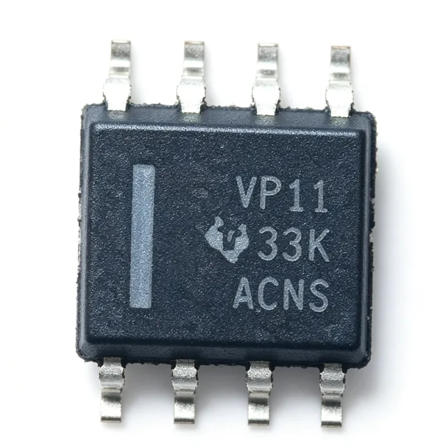
SN65HVD11 - 3.3V RS-485 Transceiver | Texas Instruments
The SN65HVD11 is a 3.3-V RS-485 transceiver from Texas Instruments that combines a 3-state differential line driver and a differential input line receiver in a single 8-pin SOIC package. It operates from a single 3.3-V power supply and is designed for balanced transmission lines, meeting or exceeding ANSI TIA/EIA-485-A and ISO 8482:1993 standards. The device supports data rates up to 10 Mbps and features bus-pin ESD protection exceeding 16 kV HBM, making it robust for industrial and building automation networks. RS-485 is a standard for serial communication systems that use differential signaling to transmit data over long distances and in noisy environments. The SN65HVD11 belongs to the family of RS-485 transceivers, which are essential components in industrial control networks, building automation, and other multi-point data acquisition systems. These transceivers convert logic-level signals to differential voltages that can be transmitted over twisted-pair cables, providing immunity to common-mode noise and enabling communication over distances up to 1200 meters. Key features of the SN65HVD11 include a 1/8 unit-load option that allows up to 256 transceivers on a single bus, a wide common-mode input range of -7 V to +12 V, and a low quiescent current of 1.1 mA typical. The device also features thermal shutdown protection and a 3-state output for bus sharing. The 8-pin SOIC package (D) is industry-standard, ensuring compatibility with existing PCB layouts. The SN65HVD11 uses a Power BiCMOS process, which combines low power consumption with high-speed operation. The differential driver outputs a minimum of 1.5 V across a 54-ohm load, while the receiver has a sensitivity of ±200 mV. The device is specified for operation over the industrial temperature range of -40°C to +85°C, making it suitable for harsh environments. Typical applications include industrial automation, building automation, HVAC systems, and point-of-sale terminals. The SN65HVD11 is also used in motor control and power inverter systems where reliable communication over long distances is required. Its high ESD protection and wide common-mode range make it ideal for factory floor networks. When designing with the SN65HVD11, ensure proper termination (120-ohm) at both ends of the bus and use a bias network to maintain a defined idle state. The driver enable (DE) and receiver enable (RE) pins allow for half-duplex operation, and the device can be placed in a low-power shutdown mode by driving both pins high.
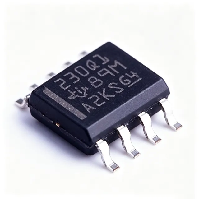
SN65HVD230QDRQ1 - 3.3V CAN Transceiver AEC-Q100 | Texas Instruments
The Texas Instruments SN65HVD230QDRQ1 is an automotive-catalog 3.3-V CAN bus transceiver with standby mode, delivering data rates up to 1 Mbps in an 8-pin SOIC (D) package qualified to AEC-Q100 for automotive applications. A controller area network (CAN) transceiver is a physical-layer interface IC that converts the logic-level TXD and RXD signals of a CAN controller into the differential CANH and CANL bus signals defined by the ISO 11898-2 High Speed CAN Physical Layer standard. Within the interface IC hierarchy, it sits between the protocol controller and the twisted-pair bus, providing driver, receiver, ESD protection, and fault-tolerance functions for the network node. Key features include ISO 11898-2 compatibility, a low-current standby mode drawing approximately 370 uA typical, bus-pin ESD protection exceeding 15 kV HBM (exceeding 2000 V per MIL-STD-883 on the device), controlled driver output transition times for improved signal quality, and a dominant-timeout feature. An unpowered node does not disturb the bus, and the RS pin selects slew-rate control or low-power mode. The SN65HVD230Q family (SN65HVD230Q, SN65HVD231Q, SN65HVD232Q) was designed to pair directly with TI TMS320Lx240x 3.3-V DSPs with on-chip CAN controllers, and also serves as a low-power replacement for the classic PCA82C250 footprint. Operating from a single 3.3-V rail eliminates level shifting when the host MCU or DSP is a 3.3-V device, reducing BOM count and board area in automotive body electronics, gateway modules, and industrial CAN nodes. Typical applications include automotive body control modules, battery management systems with 3.3-V MCUs, industrial 3.3-V CAN networks, and building automation nodes where a 5-V supply is unavailable. Design consideration: the RS pin mode selection determines standby and sleep behavior - drive or tie it so the node can wake the transceiver from its 370 uA standby state when bus activity resumes, and provide a 4.7 kOhm to 10 kOhm split-termination network on CANH/CANL per ISO 11898-2 layout practice. This page synthesizes verified distributor pricing, same-package drop-in alternatives, and practical design notes not found in the manufacturer datasheet.

SN65HVD234QDRQ1 - 3.3V Automotive CAN Transceiver | Texas Instruments
The Texas Instruments SN65HVD234QDRQ1 is a 3.3-V automotive-qualified CAN bus transceiver that delivers up to 1 Mbps data rate in an 8-pin SOIC (D) package. Operating from a 3 V to 3.6 V supply with a typical operating current of 6 mA, it is AEC-Q100 qualified and designed to interface a CAN controller with the physical bus in 3.3-V automotive and industrial systems. A CAN (Controller Area Network) transceiver is a physical-layer interface IC that converts the TTL-level TX and RX signals of a CAN controller into the differential CANH/CANL bus signals defined by ISO 11898. Positioned between the protocol controller and the twisted-pair bus in the system hierarchy, the transceiver determines bus robustness, fault tolerance, and power consumption of the entire CAN node. Key features include a 1 Mbps maximum signaling rate, fault-protected bus pins, and the SN65HVD234-Q1 variant's ultralow-current sleep mode: applying a low level to the EN pin (pin 5) disables both driver and receiver, drastically reducing node current consumption for battery-connectedECU domains. The device wakes when a high logic level is reapplied to pin 5. The SN65HVD233-Q1, SN65HVD234-Q1, and SN65HVD235-Q1 family members share pinout and package, differing mainly in feature set. The architecture includes an internal TXD-to-RS pin loopback that assists the CAN controller with baud-rate detection (autobaud function), simplifying firmware in systems where the bus speed is not fixed. Differential driver and receiver stages provide common-mode bus tolerance suitable for harsh automotive electrical environments. Typical applications include automotive body control modules, instrument clusters, gateway ECUs, and industrial 3.3-V CAN nodes where low-voltage logic directly interfaces the CAN controller (e.g., 3.3-V MCUs such as TMS320F280xx and MSPM0 devices) without level shifting. Design tip: respect the 3.6 V absolute maximum supply and place a 0.1 uF decoupling capacitor directly at VCC; control the EN pin carefully during startup to avoid unintended bus dominant states.