Mga Interface IC
Subkategorya
Mga Produkto (320+)

SN65HVD10P - 3.3V 32Mbps RS-485 | Texas Instruments
The Texas Instruments SN65HVD10P is a 3.3 V half-duplex RS-485 transceiver rated for 32 Mbps signaling and housed in an 8-pin PDIP (P) package. It combines a three-state differential line driver with a differential receiver in one IC, allowing a design to transmit and receive over the same balanced RS-485 bus. The device operates from a single 3.3 V supply and is specified over -40 °C to +85 °C. An RS-485 transceiver is an interface IC that converts logic-level signals into differential voltages for a balanced communication bus and converts received differential voltages back into CMOS-compatible logic. The RS-485 interface belongs to the interface-IC hierarchy and supports robust, multipoint data links used in industrial automation, instrumentation, building controls, and communications equipment. Differential signaling improves noise immunity by comparing the voltage between two conductors rather than relying on a signal measured against ground. The SN65HVD10P supports operation at 32 Mbps, making it suitable for data links that require substantially more signaling speed than conventional low-speed RS-485 equipment. Its three-state driver permits the bus driver to be disabled when the node is not transmitting. Available bus-pin ESD protection exceeds 16 kV using the HBM test method, according to the retrieved technical description. The family also provides a 1/8-unit-load option capable of supporting as many as 256 nodes on a bus. The device is designed for balanced transmission lines and meets or exceeds ANSI TIA/EIA-485-A and ISO 8482:1993 requirements, as stated on the Texas Instruments family page. This makes it applicable to both industrial control networks and shorter, high-speed interconnects where point-to-point communication is suitable. Because its package is through-hole PDIP rather than a surface-mount package, the SN65HVD10P is particularly convenient for prototypes, leaded industrial assemblies, and designs that favor easy inspection or rework. Typical uses include industrial sensor gateways, factory automation controllers, building-automation nodes, instrumentation links, and communication ports that exchange data at rates up to 32 Mbps. Half-duplex operation means the connected nodes share the bus and must avoid transmitting simultaneously. The bus direction can be controlled by a host or network controller, while receiver logic remains available for monitoring the bus according to the system architecture. PCB implementation should preserve the differential pair as a continuous, impedance-controlled route from the transceiver to the bus connector. Place termination, biasing, protection, and any required isolation close to their associated bus nodes, and route the pair away from switching nodes and high-current paths. Because the verified source data does not provide the complete pin table or recommended external-component values, those details should be confirmed in the manufacturer datasheet before layout release. This product page consolidates verified manufacturer specifications, distributor availability references, same-family drop-in candidates, and practical RS-485 design considerations. It also distinguishes confirmed parameters from information that still requires engineering review, helping designers evaluate the SN65HVD10P for industrial, automation, and high-speed balanced-bus applications.
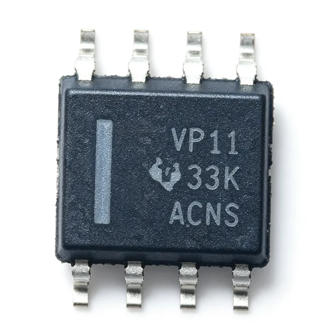
SN65HVD11 - 3.3V RS-485 Transceiver | Texas Instruments
The SN65HVD11 is a 3.3-V RS-485 transceiver from Texas Instruments that combines a 3-state differential line driver and a differential input line receiver in a single 8-pin SOIC package. It operates from a single 3.3-V power supply and is designed for balanced transmission lines, meeting or exceeding ANSI TIA/EIA-485-A and ISO 8482:1993 standards. The device supports data rates up to 10 Mbps and features bus-pin ESD protection exceeding 16 kV HBM, making it robust for industrial and building automation networks. RS-485 is a standard for serial communication systems that use differential signaling to transmit data over long distances and in noisy environments. The SN65HVD11 belongs to the family of RS-485 transceivers, which are essential components in industrial control networks, building automation, and other multi-point data acquisition systems. These transceivers convert logic-level signals to differential voltages that can be transmitted over twisted-pair cables, providing immunity to common-mode noise and enabling communication over distances up to 1200 meters. Key features of the SN65HVD11 include a 1/8 unit-load option that allows up to 256 transceivers on a single bus, a wide common-mode input range of -7 V to +12 V, and a low quiescent current of 1.1 mA typical. The device also features thermal shutdown protection and a 3-state output for bus sharing. The 8-pin SOIC package (D) is industry-standard, ensuring compatibility with existing PCB layouts. The SN65HVD11 uses a Power BiCMOS process, which combines low power consumption with high-speed operation. The differential driver outputs a minimum of 1.5 V across a 54-ohm load, while the receiver has a sensitivity of ±200 mV. The device is specified for operation over the industrial temperature range of -40°C to +85°C, making it suitable for harsh environments. Typical applications include industrial automation, building automation, HVAC systems, and point-of-sale terminals. The SN65HVD11 is also used in motor control and power inverter systems where reliable communication over long distances is required. Its high ESD protection and wide common-mode range make it ideal for factory floor networks. When designing with the SN65HVD11, ensure proper termination (120-ohm) at both ends of the bus and use a bias network to maintain a defined idle state. The driver enable (DE) and receiver enable (RE) pins allow for half-duplex operation, and the device can be placed in a low-power shutdown mode by driving both pins high.

SN65HVD11D - 3.3V RS-485 Transceiver | Texas Instruments
The Texas Instruments SN65HVD11D is a 3.3 V differential transceiver combining a three-state differential line driver and a differential line receiver in an 8-pin SOIC package. The device supports RS-485 and RS-422 balanced transmission applications, uses a single 3.3 V supply, and provides a one-eighth unit-load option supporting up to 256 nodes. Bus-pin ESD protection exceeds 16 kV HBM, making the part suitable for industrial equipment exposed to electrostatic discharge on external communication lines. A differential transceiver is an interface IC that transmits and receives data across a balanced pair of conductors. The driver converts a single-ended logic input into complementary differential outputs, while the receiver converts the differential bus voltage into a single-ended logic output. In the RS-485 hierarchy, the SN65HVD11D belongs to the class of multipoint differential bus interface ICs used by industrial automation, test equipment, building controls, and communications equipment. Key features include operation from a 3.3 V power supply, three-state driver output, differential receive capability, one-eighth unit-load operation, and bus-pin ESD protection exceeding 16 kV HBM. The low unit loading allows multiple nodes to share a bus while controlling the loading presented by each receiver. The three-state output also permits multiple drivers to be connected to a shared bus when only one driver is enabled at a time. The SN65HVD11D family is designed for balanced transmission lines and is stated to meet or exceed ANSI TIA/EIA-485-A and ISO 8482:1993. Its differential signaling improves noise immunity by deriving the receiver decision from the voltage difference between the A and B conductors rather than from either conductor relative to ground. This makes it appropriate for longer cable runs and electrically noisy factory environments when implemented with proper termination and biasing. Typical uses include industrial RS-485 multidrop buses, factory sensor networks, building-automation controllers, instrument interfaces, and point-to-point RS-422 links. The eight-pin SOIC package supports conventional surface-mount assembly, while the low unit loading helps preserve bus loading margin as more nodes are added. PCB design should provide a continuous return or reference path, route the differential pair together with matched spacing, and place termination and fail-safe bias components at physically appropriate bus locations. The supply should be decoupled close to the device, and unused digital inputs should not float. Bus protection, surge-current requirements, and cable length must be checked against the complete system rather than inferred from the transceiver rating alone. This page combines verified manufacturer and distributor information, practical RS-485 design guidance, a same-package alternative comparison, and structured selection criteria. These details help engineers distinguish genuine footprint-compatible options from parts that only provide similar RS-485 functionality.
SN65HVD12D - 3.3V RS-485 Transceiver | Texas Instruments
Texas Instruments SN65HVD12D is a 3.3 V differential transceiver for half-duplex RS-422 and RS-485 balanced communications, housed in an 8-pin SOIC package. It combines a 3-state differential line driver with a differential line receiver and supports a maximum signaling rate of 1 Mbit/s. The device provides bus-pin ESD protection exceeding 16 kV HBM and is offered in a 1/8 unit-load option supporting up to 256 nodes on a bus. An RS-485 transceiver is an interface IC that converts logic-level signals into balanced differential signals for reliable communication over long, noise-prone industrial cabling. The SN65HVD12 belongs to the RS-485 transceiver hierarchy, which includes half-duplex driver/receiver combinations and is widely used where multiple nodes share a two-wire bus. Its differential signaling improves common-mode rejection by comparing the voltage between two conductors rather than referencing the signal to ground. The SN65HVD12D operates from a single 3.3 V supply and supports both RS-422 and RS-485 networks. Its 3-state driver output can be disabled when the device is not transmitting, allowing multiple drivers to share the same bus. The 1 Mbit/s maximum data rate supports moderate-speed industrial links, while the low unit load permits a comparatively large number of connected nodes. Bus-pin ESD protection exceeding 16 kV HBM improves robustness during installation and industrial handling. According to the Texas Instruments manufacturer datasheet and product page, the SN65HVD12 family meets or exceeds ANSI TIA/EIA-485-A and ISO 8482:1993 requirements. The SN65HVD12D is a half-duplex, one-transmitter, one-receiver device in the 8-SOIC package. Its balanced differential driver and receiver make it appropriate for point-to-point RS-422 links and multipoint RS-485 buses when node count, cable length, topology, and termination remain within the applicable network design limits. Typical uses include industrial automation controllers, sensor gateways, building automation equipment, factory data acquisition, motor-control interfaces, and embedded serial buses. The 3.3 V supply aligns with modern controller logic levels, while the 1/8 unit-load option allows multiple low-power nodes to share a bus. The same-package footprint and 3.3 V operating class can simplify replacement evaluation when comparing qualified RS-485 transceivers for an existing 8-SOIC board. Designers should provide correct bus biasing, termination, protection, and grounding rather than relying on the transceiver alone for network reliability. Place the transceiver close to the connector, route the differential pair as a tightly coupled pair, and minimize stub lengths. Verify that external protection devices clamp transients within the device ratings and confirm driver-enable and receiver-enable timing in the system firmware. This page combines verified manufacturer and distributor information with same-package replacement guidance, application-specific design notes, and a parameter comparison. It distinguishes documented drop-in candidates from choices that require package, logic, speed, or qualification review, helping engineers preserve PCB compatibility while evaluating supply and lifecycle risk.
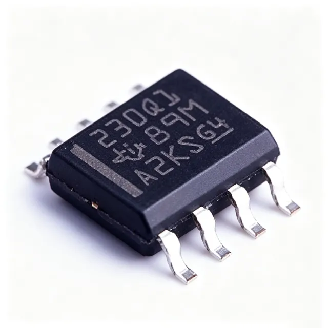
SN65HVD230QDRQ1 - 3.3V CAN Transceiver AEC-Q100 | Texas Instruments
The Texas Instruments SN65HVD230QDRQ1 is an automotive-catalog 3.3-V CAN bus transceiver with standby mode, delivering data rates up to 1 Mbps in an 8-pin SOIC (D) package qualified to AEC-Q100 for automotive applications. A controller area network (CAN) transceiver is a physical-layer interface IC that converts the logic-level TXD and RXD signals of a CAN controller into the differential CANH and CANL bus signals defined by the ISO 11898-2 High Speed CAN Physical Layer standard. Within the interface IC hierarchy, it sits between the protocol controller and the twisted-pair bus, providing driver, receiver, ESD protection, and fault-tolerance functions for the network node. Key features include ISO 11898-2 compatibility, a low-current standby mode drawing approximately 370 uA typical, bus-pin ESD protection exceeding 15 kV HBM (exceeding 2000 V per MIL-STD-883 on the device), controlled driver output transition times for improved signal quality, and a dominant-timeout feature. An unpowered node does not disturb the bus, and the RS pin selects slew-rate control or low-power mode. The SN65HVD230Q family (SN65HVD230Q, SN65HVD231Q, SN65HVD232Q) was designed to pair directly with TI TMS320Lx240x 3.3-V DSPs with on-chip CAN controllers, and also serves as a low-power replacement for the classic PCA82C250 footprint. Operating from a single 3.3-V rail eliminates level shifting when the host MCU or DSP is a 3.3-V device, reducing BOM count and board area in automotive body electronics, gateway modules, and industrial CAN nodes. Typical applications include automotive body control modules, battery management systems with 3.3-V MCUs, industrial 3.3-V CAN networks, and building automation nodes where a 5-V supply is unavailable. Design consideration: the RS pin mode selection determines standby and sleep behavior - drive or tie it so the node can wake the transceiver from its 370 uA standby state when bus activity resumes, and provide a 4.7 kOhm to 10 kOhm split-termination network on CANH/CANL per ISO 11898-2 layout practice. This page synthesizes verified distributor pricing, same-package drop-in alternatives, and practical design notes not found in the manufacturer datasheet.

SN65HVD234QDRQ1 - 3.3V Automotive CAN Transceiver | Texas Instruments
The Texas Instruments SN65HVD234QDRQ1 is a 3.3-V automotive-qualified CAN bus transceiver that delivers up to 1 Mbps data rate in an 8-pin SOIC (D) package. Operating from a 3 V to 3.6 V supply with a typical operating current of 6 mA, it is AEC-Q100 qualified and designed to interface a CAN controller with the physical bus in 3.3-V automotive and industrial systems. A CAN (Controller Area Network) transceiver is a physical-layer interface IC that converts the TTL-level TX and RX signals of a CAN controller into the differential CANH/CANL bus signals defined by ISO 11898. Positioned between the protocol controller and the twisted-pair bus in the system hierarchy, the transceiver determines bus robustness, fault tolerance, and power consumption of the entire CAN node. Key features include a 1 Mbps maximum signaling rate, fault-protected bus pins, and the SN65HVD234-Q1 variant's ultralow-current sleep mode: applying a low level to the EN pin (pin 5) disables both driver and receiver, drastically reducing node current consumption for battery-connectedECU domains. The device wakes when a high logic level is reapplied to pin 5. The SN65HVD233-Q1, SN65HVD234-Q1, and SN65HVD235-Q1 family members share pinout and package, differing mainly in feature set. The architecture includes an internal TXD-to-RS pin loopback that assists the CAN controller with baud-rate detection (autobaud function), simplifying firmware in systems where the bus speed is not fixed. Differential driver and receiver stages provide common-mode bus tolerance suitable for harsh automotive electrical environments. Typical applications include automotive body control modules, instrument clusters, gateway ECUs, and industrial 3.3-V CAN nodes where low-voltage logic directly interfaces the CAN controller (e.g., 3.3-V MCUs such as TMS320F280xx and MSPM0 devices) without level shifting. Design tip: respect the 3.6 V absolute maximum supply and place a 0.1 uF decoupling capacitor directly at VCC; control the EN pin carefully during startup to avoid unintended bus dominant states.
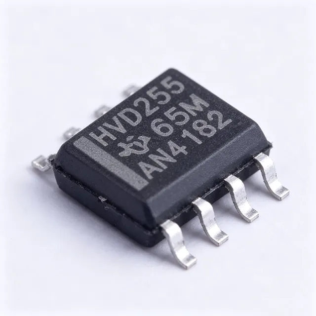
SN65HVD255DR - 1Mbps Turbo CAN Transceiver | TI
The Texas Instruments SN65HVD255DR is a Turbo CAN transceiver designed for highly loaded Controller Area Network (CAN) networks with data rates in excess of 1 Mbps. It is packaged in an 8-pin SOIC (D) surface-mount package and operates over an extended temperature range of -40C to +125C, implementing the ISO 11898-2 High-Speed CAN physical layer standard. A CAN transceiver is the physical-layer interface between a CAN protocol controller and the twisted-pair bus, converting controller TXD/RXD logic signals into differential CANH/CANL signals. Within the CAN system hierarchy (application layer, protocol controller, transceiver, bus), the transceiver provides the drive strength, common-mode tolerance, and ESD/fault robustness required for reliable communication in harsh electrical environments. Key features include fast loop propagation times that enhance timing margins on long, heavily loaded networks; functional-safety-oriented features per the TI datasheet; dominant and recessive output drive compliant with ISO 11898-2; and internal protection including thermal shutdown and short-circuit current limiting. The device operates from a nominal 5V supply. Low electromagnetic emission and high immunity make it suitable for demanding automotive and industrial buses. Typical applications include industrial automation and motor drives, building and climate control automation, security systems, and telecom base station status and control networks. In these systems the Turbo CAN fast loop times allow more nodes, longer cable runs, or higher bit rates than standard transceivers. When designing with the SN65HVD255DR, terminate both bus ends with 120-ohm resistors, place a 0.1uF bypass capacitor close to VCC, and keep the CANH/CANL traces symmetric and short to preserve signal integrity at extended data rates.
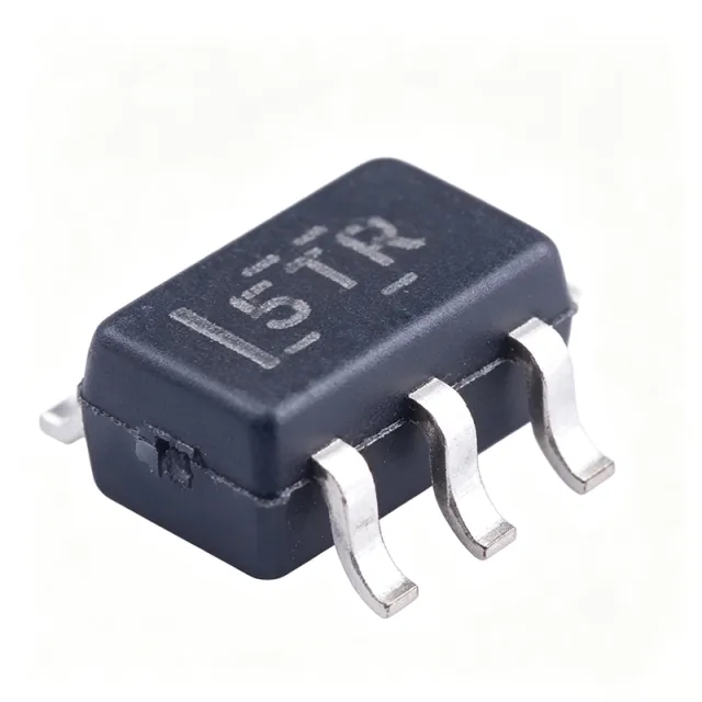
SN65HVD255QDRQ1 - 3.3V Turbo CAN Transceiver Q1 | TI
The Texas Instruments SN65HVD255QDRQ1 is an AEC-Q100 qualified 3.3V Turbo CAN transceiver delivering data rates in excess of 1 Mbps with fast loop times, housed in an 8-pin SOIC (D) package for highly loaded automotive and industrial CAN networks. A CAN transceiver is a physical-layer interface device that converts the single-ended TTL logic levels of a CAN protocol controller into the differential signaling on a twisted-pair CAN bus, and back again at the receiver. Within the interface IC hierarchy, it sits between the CAN controller (often integrated in an MCU) and the two-wire physical bus, providing dominant/recessive driving, bus fault protection, and receiver filtering. Key features include turbo-mode operation supporting data rates beyond 1 Mbps on short networks, enhanced loop-time symmetry for large and heavily loaded networks, single-supply 3.3V operation, and ISO 11898 physical-layer compatibility. The device integrates short-circuit protection, thermal shutdown, and wide common-mode bus voltage tolerance for robust operation in harsh electrical environments. The proprietary transceiver architecture of the SN65HVD25x Turbo family delivers fast loop times that improve arbitration success and bit-timing margin in highly loaded network nodes, distinguishing it from standard 1 Mbps transceivers. Receiver input impedance and bus biasing are optimized for large networks with many nodes, and the family datasheet (Rev. D) adds features oriented toward functional safety. The RS pin selects between slope-control and high-speed (turbo) operation, letting one design cover both EMC-sensitive and maximum-speed segments. Typical applications include automotive body electronics and gateway nodes, industrial PLC and motor-control CAN networks running at 3.3V logic, and high-data-rate buses where standard transceivers cannot sustain signal integrity above 1 Mbps. Design tip: size the bus termination at 120 ohms, verify dominant-state current limits when operating in turbo mode, and place a 0.1 uF local decoupling capacitor at VCC. This page synthesizes verified distributor pricing, drop-in alternatives, pinout data, and practical design notes not found in the manufacturer datasheet alone. Prices referenced as of 2026-09-01.
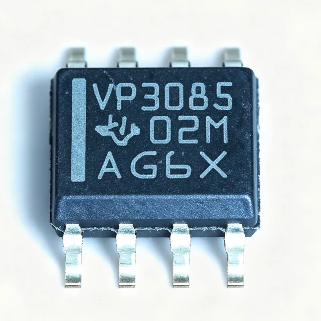
SN65HVD3085EDR - 5V Half-Duplex RS-485 Transceiver | TI
The Texas Instruments SN65HVD3085EDR is a low-power, half-duplex RS-485 transceiver in an 8-pin SOIC (D) package, powered from a single 5V supply and fully compliant with the TIA/EIA-485A standard. It integrates one driver and one receiver for bidirectional communication on twisted-pair data bus networks, with controlled transition times suited to long cable runs. An RS-485 transceiver is a differential line interface IC that converts single-ended logic signals into balanced differential signals for robust serial communication. Within the interface IC hierarchy, it sits between a UART/MCU and the physical twisted-pair bus, providing the electrical drive, receiver threshold, and bus-fault tolerance defined by the TIA/EIA-485A standard. Key features include operation from a 4.5V to 5.5V supply, signaling rates up to 20 Mbps (per the SNx5HVD308xE family data), a small SOIC-8 footprint, and an operating temperature range of -40C to +85C. Controlled driver output transition times reduce EMI and reflections, while the low-power design minimizes quiescent supply current for multi-node networks. Architecturally, the device uses a differential driver with three-state outputs and a differential receiver with fail-safe inputs. Driver (DE) and receiver enable (/RE) pins allow half-duplex direction control from a standard MCU GPIO. Bus pins A and B tolerate the fault conditions required by the RS-485 standard, supporting reliable operation in electrically noisy industrial environments. Typical applications include industrial automation and Modbus RTU networks, building and HVAC control buses, battery-management and motor-control communication links, and point-to-multipoint serial links over twisted pair. The 20 Mbps class speed also suits fast industrial backbones needing short frame times. Design tip: use fail-safe biasing resistors on the A/B bus lines and terminate both cable ends with 120 ohm resistors to prevent reflections and receiver chatter on idle buses. This page synthesizes distributor pricing, drop-in alternatives, pinout data, and practical design notes not consolidated in the manufacturer datasheet. Pricing references as of 2026-08-29 (LCSC from $0.3185).
SN65HVD78D - 3.3V 50Mbps Half-Duplex RS-485 | TI
The Texas Instruments SN65HVD78D is a 3.3 V half-duplex RS-485 transceiver with one differential driver, one differential receiver, 50 Mbps signaling, and IEC ESD protection, housed in an 8-pin SOIC package. Its 3 V to 3.6 V supply range, -40°C to +125°C operating range, and robust bus-pin protection suit demanding industrial communication systems. An RS-485 transceiver is a physical-layer interface IC that combines a differential line driver and receiver for bidirectional data transfer over a balanced bus. The half-duplex arrangement allows the same differential pair to support transmission and reception, although the design must control bus direction so that multiple drivers do not contend on the bus. Within the broader hierarchy, this device is an RS-485 interface IC, a wired-network transceiver, and a semiconductor. Key features include 50 Mbps maximum signaling, a 3.3 V nominal supply, one driver and one receiver, half-duplex operation, and enhanced ESD protection on the bus pins. The manufacturer describes protection against both Human Body Model and IEC Contact Discharge events. These characteristics distinguish the SN65HVD78D from slower RS-485 transceivers intended for lower-speed industrial multidrop networks. The combination of a differential driver and receiver on a single 3.3 V supply supports compact point-to-point and multidrop bus implementations. Half-duplex communication reduces the number of signal conductors, while the 50 Mbps capability allows the physical layer to carry high-speed command, measurement, or control traffic. The SOIC-8 package also supports conventional surface-mount assembly and is compatible with automated production equipment. Typical applications include industrial factory automation, industrial sensor and actuator networks, building-control equipment, robotics, test and measurement systems, and embedded industrial controllers. The device is especially appropriate where a 3.3 V system requires a compact, high-speed RS-485 physical layer and where exposed bus connections increase ESD risk. Designers should verify driver-enable sequencing, termination, fail-safe behavior, and signal-integrity margins against the complete bus topology. The 3.3 V supply must remain within 3 V to 3.6 V, and exposed RS-485 conductors may still require external surge and common-mode protection beyond the device's specified ESD capability. This page consolidates manufacturer information, verified distributor listings, drop-in comparison options, and practical design guidance. It distinguishes confirmed ratings from parameters that still require consultation of the complete manufacturer datasheet before production release.
SN65HVD82D - 5V RS-485 Transceiver with IEC ESD | TI
The Texas Instruments SN65HVD82D is a 5-V half-duplex RS-422/RS-485 transceiver with IEC ESD protection, offered in an 8-pin SOIC package. It combines one differential driver and one differential receiver on a single 5-V supply, making it suitable for industrial bidirectional serial networks where both transmission and reception are required on the same bus pair. An RS-485 transceiver is an interface IC that converts logic-level signals into differential bus signals and converts received differential signals back into logic levels. As a member of the RS-422 and RS-485 interface hierarchy, it supports noise-resistant, point-to-point or multipoint communication over longer cable runs than conventional single-ended interfaces. The half-duplex arrangement allows a connected node to transmit and receive, but not simultaneously, on the same pair of conductors. The SN65HVD82D operates from a single 5-V supply and supports data rates up to 250 kbps according to the available FindIC product listing. Its bus pins are designed for robust ESD event handling, with manufacturer and distributor descriptions identifying Human-Body Model, Air-Gap Discharge, Contact Discharge, and IEC ESD protection. The 8-pin SOIC package provides a conventional surface-mount form factor for industrial communication equipment. Internally, the device combines a differential driver with a differential receiver rather than implementing two unrelated interface channels. This arrangement supports bidirectional data transfer when the design uses a direction-control signal, bus multiplexing, or an application-specific enable strategy. Because RS-485 is a differential bus, correct termination, biasing, grounding, and cable routing remain central to achieving reliable communication. Typical uses include industrial sensor networks, factory automation equipment, building-control interfaces, process-monitoring systems, and communications equipment that connects a controller to remote nodes. The device is also relevant to laboratory and test systems where a compact 5-V RS-485 interface is required close to a digital controller. When laying out a board around the SN65HVD82D, place its decoupling capacitor close to the supply pins and route the differential bus as a tightly coupled pair. External protection may still be appropriate when exposed cables or severe industrial transients are expected, because integrated ESD protection does not remove the need for a correctly engineered cable and grounding system. This page combines the verified manufacturer, distributor, and cross-reference information with a practical view of package compatibility, pricing availability, ESD considerations, and application guidance. It also distinguishes verified facts from electrical details that still require confirmation in the latest manufacturer datasheet before final design release.

SN65LVDS100DGK - 2Gbps LVDS/LVPECL/CML Buffer | TI
The Texas Instruments SN65LVDS100DGK is a 2-Gbps LVDS, LVPECL and CML to LVDS buffer, repeater and level translator in an 8-pin VSSOP (DGK) package, rated for operation from -40C to +85C on a 3.3V supply. It regenerates high-speed differential data streams by connecting a high-speed differential receiver directly to a high-speed differential driver, restoring signal edge rates and amplitude on long or heavily loaded LVDS links. A differential buffer, repeater or translator is an interface IC that sits in a high-speed serial signal path: its receiver accepts one differential logic family (LVDS, PECL/LVPECL or CML) and its driver re-transmits the same data as clean LVDS. In the signal-integrity hierarchy, it sits between physical transceivers and transmission media such as backplanes, cables and clock trees, where signal degradation would otherwise exceed receiver margin. Key features include operation at signaling rates of 2 Gbps and above, low 100 ps maximum part-to-part skew, 25 mV of receiver input threshold hysteresis over a 0V to 4V common-mode input range, and positioning as a low-power alternative to the MC100EP16 ECL receiver. The wide input common-mode range allows it to accept LVPECL and CML levels while always driving a standard LVDS output. Technically, the SN65LVDS100 is formed from an input differential receiver with hysteresis followed by an LVDS output driver compliant with EIA/TIA-644 (LVDS) signaling. The device supports an additional VBB reference output of typically 1.35V below VCC, which is particularly useful for receiving single-ended 3.3V PECL inputs. Total jitter is specified for signaling rates up to 2 Gbps, and ESD tolerance exceeds 2000V per the human-body-model test referenced on the product page. Typical applications include clock distribution and jitter cleaning in networking and telecom line cards, backplane signal re-driving in industrial automation, and high-speed point-to-point links between FPGAs, ASICs and serializers where input signal quality has degraded after long traces or connectors. Design-wise, maintain a solid 3.3V supply with low-inductance 0.1uF plus 10uF decoupling, keep differential traces impedance-controlled at 100 ohms, and remember the maximum supply range of 3V to 3.6V. Place the part close to connectors to maximize the regenerated link margin. This page synthesizes distributor pricing, drop-in alternative cross-references, and practical design notes not found in the manufacturer datasheet, with pricing as of 2026-10-19.
SN65LVDS100DGKR - 2Gbps LVDS/LVPECL/CML Repeater | TI
The Texas Instruments SN65LVDS100DGKR is a 2-Gbps LVDS, LVPECL and CML to LVDS differential buffer, repeater and translator housed in an 8-pin VSSOP (DGK) package, rated for operation from -40C to +85C. A differential repeater is an interface IC that receives a high-speed differential signal, regenerates it through an internal receiver-driver chain, and retransmits a clean copy on the output side. In the signal-chain hierarchy, repeaters sit between the physical differential line (per EIA/TIA-644 LVDS and related PECL/CML standards) and the end receiver, restoring degraded amplitude and edge quality on long backplanes, cables, and clock-distribution networks. Key features include signaling rates up to 2 Gbps, low part-to-part skew (100 ps max class), and a built-in VBB bias output of typically 1.35 V below VCC, which lets the receiver accept single-ended 3.3 V PECL inputs directly. The device is also positioned by TI as a low-power alternative to the MC100EP16 ECL buffer, and is qualified for automotive applications. Inside, a high-speed differential receiver with input hysteresis accepts LVDS, LVPECL, or CML levels and drives an LVDS-compliant differential output, effectively decoupling the transmit side from input-level variations. This level translation removes the need for external bias networks or level-shifting discretes, reducing BOM count and jitter contribution compared with cascaded discrete buffers. Typical applications include clock and data signal regeneration in telecom and networking line cards, PCIe/serial-link signal integrity recovery on long PCB traces, and test-and-measurement signal distribution where 2-Gbps edges must be preserved. The automotive qualification also supports infotainment and camera-link repeater use. For design, decouple VCC with at least 0.1 uF ceramic capacitors close to the supply pins, route the differential pair with controlled impedance (100 ohm LVDS), and keep the VBB bypass path quiet for single-ended PECL use. This page synthesizes distributor pricing (LCSC, DigiKey, Mouser), drop-in same-package alternatives, and design notes that go beyond the raw datasheet parameters.
SN65LVDS100DGKRG4 - 2Gbps LVDS Repeater | TI | VSSOP-8
The Texas Instruments SN65LVDS100DGKRG4 is a 2 Gbps LVDS/LVPECL/CML-to-LVDS differential repeater and translator in an 8-pin VSSOP (DGK) package. It regenerates high-speed differential signals with only 65 ps of total jitter, making it a clean-signal solution for long backplane or cable runs. A differential repeater is a signal-conditioning device placed in a high-speed serial link: it receives a degraded differential waveform, re-amplifies and re-times it through a receiver-driver pair, and launches a fresh LVDS signal onto the next segment. In the signal-integrity hierarchy it sits between a plain buffer and a full retimer, belonging to the broader family of interface ICs and signal buffers/repeaters. Key features include signaling rates up to 2 Gbps, low 100 ps maximum part-to-part skew, receiver input threshold hysteresis for noise rejection, and a wide input common-mode range that accepts LVDS, PECL, and CML signal levels. TI positions it as a low-power alternative to the MC100EP16 ECL repeater, offering significant static current savings in LVDS mode. The input receiver tolerates a broad common-mode range, so designers can AC-couple or DC-couple LVPECL and CML sources with simple biasing. The output drives a nominally 100-ohm differential transmission line with standard LVDS levels. The signal path is always-on: power is roughly the sum of receiver and driver currents, and the DGK package junction-to-ambient thermal resistance comfortably handles the sub-100 mW dissipation. Typical applications include clock distribution and fan-out in telecom line cards, redriving LVDS signals across backplanes and cable interconnects, and translating PECL or CML outputs to LVDS-compatible receivers in test instrumentation and imaging systems. For design, keep the 100-ohm differential impedance continuous through the device; place the part at the midpoint of lossy traces where the eye is still open enough to meet the receiver threshold. AC-coupled PECL inputs require appropriate bias resistors per the TI datasheet application section. This page synthesizes distributor pricing, drop-in same-family alternatives, and practical design notes not found in the manufacturer datasheet.

SN65LVDS22DR - Dual Multiplexed LVDS Repeater 250Mbps | TI
The Texas Instruments SN65LVDS22DR is a dual multiplexed LVDS repeater that supports clock rates to 200 MHz (400 Mbps) and data rates to 250 Mbps, operates from a single 3.3 V supply, and is housed in a 16-pin SOIC (D) package. An LVDS (Low-Voltage Differential Signaling) repeater is an interface buffer that regenerates and redistributes differential signal pairs, restoring signal amplitude and edge quality degraded by long backplanes, cables, or multiple loads. As a member of the broader voltage-mode driver and interface IC family, an LVDS repeater sits between a differential transmitter and receiver in the signal chain hierarchy, isolating loading effects and enabling fan-out of a single LVDS source to multiple destinations without signal degradation. Key features include ANSI TIA/EIA-644-1995 standard compliance, LVDS output voltages of 350 mV into a 100-ohm load, and a typical propagation delay of 4 ns. ESD protection exceeds 12 kV on bus pins and exceeds 2000 V per MIL-STD-883, Method 3015 (HBM), with machine-model protection exceeding 200 V (200 pF, 0 ohm). The device is pin compatible with the SN65LVDS122 and SN65LVDT122 1.5 Gbps 2x2 crosspoint switches from TI, providing a direct speed-upgrade path. The multiplexed 1x2:2 architecture allows each LVDS input to be selectively routed or repeated, giving system designers flexible signal-distribution topologies. Low differential output swing (typically 350 mV) minimizes EMI and power consumption compared with older differential standards, while the 4 ns propagation delay keeps timing budgets small even at 250 Mbps data rates. Typical applications include backplane signal buffering in industrial control systems, clock distribution in telecom and datacom line cards, and LVDS signal fan-out in automotive communication modules, where the device is qualified for automotive applications. Design considerations: TI specifies the SN65LVDS22 (100-ohm load) and SN65LVDM22 (50-ohm load) as load-specific variants, so select the termination impedance variant to match the bus. When more bandwidth is needed, drop in the pin-compatible SN65LVDS122/SN65LVDT122 for up to 1.5 Gbps operation. This page synthesizes distributor availability, drop-in alternative analysis, and practical design notes not found in the manufacturer datasheet.
SN65LVDT100DGKR - 2Gbps LVDS Repeater/Translator | Texas Instruments
The Texas Instruments SN65LVDT100DGKR is a 2-Gbps LVDS, LVPECL and CML to LVDS differential repeater/translator housed in an 8-pin VSSOP (DGK) package, rated for operation from -40C to +85C. It accepts LVDS, PECL or CML input signals at signaling rates up to 2 Gbps and repeats them as LVDS output levels on a 3.3-V supply. A differential repeater/translator is an interface IC that regenerates high-speed differential signals degraded by long transmission lines, connectors or backplanes. Within the signal-chain hierarchy, it sits between physical transceivers and their serializers or receivers: the device receives a differential waveform, squares its edges, and re-drives it with clean LVDS levels, extending the achievable link distance beyond what a plain transceiver can reach. Key features include a 2-Gbps maximum signaling rate, low total jitter (less than 65 ps per the device overview), maximum 100-ps part-to-part skew, and an integrated 110-ohm differential line-termination resistor. The on-chip termination reduces board space, component count and stub length compared with external resistor networks. The receiver input threshold hysteresis further improves noise immunity on marginal differential links. The architecture combines a high-speed differential receiver with an LVDS driver connected as a repeater. TI positions the SN65LVDT100 as a low-power alternative for the MC100EP16, while adding signal reconditioning. The integrated 7-V protected output structure tolerates hot-swap-style line conditions, and the wide input-format acceptance (LVDS/LVPECL/CML) removes the need for level-shifting front ends in mixed-logic designs. Typical applications include LVDS LCD panel links needing extra cable reach (as discussed in TI's E2E interface forum for 5-m cable runs), backplane and rack-to-rack differential clock or data distribution, and generic 2-Gbps signal reconditioning in telecommunications, industrial imaging and test equipment. When designing with this device, keep the 110-ohm integrated termination in mind when matching it to cables or boards whose characteristic impedance differs significantly from 100 ohms, and minimize stub length by placing the part directly at the connector. This page adds distributor pricing context, verified drop-in alternatives, and practical design notes not found in the manufacturer datasheet, with pricing references marked as of 2026-10-19.

SN74AVC4T245QWRGYRQ1 - 4-Bit Dual-Supply Level Shifter AEC-Q100 | TI
The Texas Instruments SN74AVC4T245QWRGYRQ1 is an automotive-grade, 4-bit dual-supply bus transceiver with configurable voltage-level translation and 3-state outputs, packaged in a compact 16-pin VQFN (RGY, 4x3.5 mm) footprint. It enables bidirectional level shifting between buses operating at different supply voltages and is AEC-Q100 qualified for automotive use. A bus transceiver is a digital interface IC that combines transmit and receive paths in one device, allowing bidirectional data flow between two buses. The SN74AVC4T245-Q1 belongs to the voltage-level translator family, a subset of interface ICs within the broader integrated circuits category. Level translation is essential when connecting components with different I/O voltages, such as a 1.8 V microcontroller interfacing with a 3.3 V peripheral. Key features include dual-supply operation with VCCA and VCCB each accepting 1.2 V to 3.6 V, tri-state outputs for bus isolation, and Ioff partial-power-down protection that disables outputs and prevents damaging backflow current when either supply is removed. A typical propagation delay of 2.1 ns and data rates up to 380 Mbps make the device suitable for SPI, I2C, UART, and parallel GPIO interfaces. The CMOS architecture supports use as two independent 2-bit transceivers or one 4-bit transceiver. Direction control (1DIR, 2DIR) and output-enable (1OE, 2OE) pins are referenced to VCCA, simplifying control-logic design in mixed-voltage systems. The device operates asynchronously, requiring no clock signal, and is fully specified over the -40C to +125C automotive temperature range. Typical applications include automotive body control modules, ADAS ECUs, infotainment systems, and industrial automation. In ECUs, it bridges 1.8 V or 2.5 V MCUs to 3.3 V sensors, CAN transceiver interfaces, SPI flash, and general-purpose GPIO level shifting. Site-available companions include the SN65HVD230QDRQ1 CAN transceiver and SN74LVC1T45QDCKRQ1 single-bit translator. Design tip: decouple VCCA and VCCB with 0.1 uF capacitors placed close to the pins, and ensure DIR/OE signals (VCCA domain) are stable before data transmission to avoid bus contention.

SN75174DW - 4-Channel RS-422/RS-485 Driver | Texas Instruments
The Texas Instruments SN75174DW is a monolithic quadruple differential line driver with four independently enabled, three-state outputs, a 4.75 V to 5.25 V supply range, and operation up to 4 megabaud in a 20-pin SOIC package. It meets the requirements of ANSI EIA/TIA-422-B, RS-485, and ITU Recommendation V.11. A differential line driver is an interface IC that converts logic-level signals into balanced differential outputs for communication over cables or long printed-circuit-board traces. As a member of the RS-422 and RS-485 interface hierarchy, it translates a digital transmitter signal into noise-resistant differential voltage pairs. The four channels suit multipoint buses, industrial equipment, industrial-control systems, and legacy data ports where multiple bus nodes require controlled output states. The SN75174 provides four differential drivers and common enable and ground pins. Each driver uses a positive and negative output, while the three-state outputs support shared party-line buses by placing unused transmitters in a high-impedance state. Its balanced outputs reduce sensitivity to common-mode noise, and the wide positive and negative output common-mode voltage ranges make it suitable for noisy industrial environments. The device supports transmission rates up to 4 megabaud and is intended for balanced multipoint communication. This makes it appropriate for RS-422 and RS-485 systems where a transmitter must support multiple drivers on one bus. The common enable control can coordinate output states, but system design must prevent multiple drivers from actively driving the same pair simultaneously. Typical uses include industrial RS-485 buses, data acquisition equipment, telecommunications interfaces, instrumentation, computer peripherals, and embedded control systems. The 20-pin SOIC package supports conventional surface-mount assembly and is available as the SN75174DW ordering option identified by DigiKey as a 20-SOIC device. Designers should match cable termination, biasing, and transceiver direction-control requirements to the bus standard. Keep traces short where possible, provide a continuous ground reference where the interface standard permits it, and verify signal polarity and enable timing before enabling the outputs. The SN75174DW is a digital interface IC, so Safe Operating Area data do not apply.
SN75174DWR - 4-Channel RS-422/RS-485 Driver | Texas Instruments (Tape & Reel)
The Texas Instruments SN75174DWR is a monolithic quadruple differential line driver with four independently enabled, three-state outputs, a 4.75 V to 5.25 V supply range, and operation up to 4 megabaud in a 20-pin SOIC package. It meets the requirements of ANSI EIA/TIA-422-B, RS-485, and ITU Recommendation V.11. A differential line driver is an interface IC that converts logic-level signals into balanced differential outputs for communication over cables or long printed-circuit-board traces. As a member of the RS-422 and RS-485 interface hierarchy, it translates a digital transmitter signal into noise-resistant differential voltage pairs. The four channels suit multipoint buses, industrial equipment, industrial-control systems, and legacy data ports where multiple bus nodes require controlled output states. The SN75174 provides four differential drivers and common enable and ground pins. Each driver uses a positive and negative output, while the three-state outputs support shared party-line buses by placing unused transmitters in a high-impedance state. Its balanced outputs reduce sensitivity to common-mode noise, and the wide positive and negative output common-mode voltage ranges make it suitable for noisy industrial environments. The device supports transmission rates up to 4 megabaud and is intended for balanced multipoint communication. This makes it appropriate for RS-422 and RS-485 systems where a transmitter must support multiple drivers on one bus. The common enable control can coordinate output states, but system design must prevent multiple drivers from actively driving the same pair simultaneously. Typical uses include industrial RS-485 buses, data acquisition equipment, telecommunications interfaces, instrumentation, computer peripherals, and embedded control systems. The 20-pin SOIC package supports conventional surface-mount assembly and is available as the SN75174DWR ordering option identified by DigiKey as a 20-SOIC device. Designers should match cable termination, biasing, and transceiver direction-control requirements to the bus standard. Keep traces short where possible, provide a continuous ground reference where the interface standard permits it, and verify signal polarity and enable timing before enabling the outputs. The SN75174DWR is a digital interface IC, so Safe Operating Area data do not apply.
SN75176ADR - RS-422/RS-485 Differential Bus Transceiver | Texas Instruments
The Texas Instruments SN75176ADR is a differential bus transceiver for bidirectional RS-422 and RS-485 communication, supplied in an 8-pin SOIC package. It combines a differential line driver with a differential receiver and supports multipoint transmission over long bus lines in noisy environments. The verified product information identifies the device as an RS-422/RS-485 interface IC with a 4.75 V to 5.25 V supply range and 3-state driver and receiver outputs. The transceiver is designed for balanced transmission lines and is reported to meet ANSI Standard EIA/TIA-422-B and ITU Recommendation V.11 requirements. SN75176ADR is the Texas Instruments orderable part number associated with the SN75176A family. The SOIC-8 package supports conventional surface-mount assembly and is suitable for industrial communication, data acquisition, factory automation, and embedded serial-interface designs. The device architecture allows the same physical bus interface to support both transmitting and receiving differential data, while the 3-state outputs permit multiple drivers to share a bus when the enable control is inactive. Its differential signaling helps reject common-mode noise present in industrial environments and reduces susceptibility to ground-potential differences between connected equipment. When designing a replacement or new board around SN75176ADR, verify the logic polarity of the receiver-enable and driver-enable controls, the termination strategy, the bus biasing arrangement, and the operating voltage at every connected node. The compact SOIC-8 footprint is widely supported by PCB libraries and compatible transceiver families. This page combines verified distributor pricing, interface standards, replacement information, and practical RS-485 design guidance.
SP232ECN-L - ±15kV ESD 5V RS-232 IC | MaxLinear
The MaxLinear SP232ECN-L is a 5 V, single-supply RS-232 line transceiver with two drivers and two receivers, enhanced ±15 kV ESD protection, and a 16-pin SOIC package. It is designed for dual-channel serial-interface equipment operating from 4.5 V to 5.5 V, with an industrial temperature option identified by the supplied distributor data as 0°C to 70°C. An RS-232 transceiver is a line-interface IC that combines digital-to-analog transmit drivers with analog-to-digital receive inputs. The SP232ECN-L belongs to the RS-232 interface family, which connects TTL/CMOS logic to the charge-balanced, bipolar signaling used by RS-232 ports. Its two drivers and two receivers support two serial channels in one package. The principal verified features include operation from a single +5 V supply, compatibility with RS-232 and V.28 protocols, 2/2 transceiver organization, and enhanced ESD tolerance identified in the supplied search results as ±15 kV. The device is available from the verified distributor pages in a 16-pin SOIC package, and the results describe it as a CMOS line transceiver with TTL-compatible interfacing. The SP232ECN-L is suitable for industrial and embedded systems that need a compact, dual-channel RS-232 port without a separate driver and receiver IC for each direction. Typical uses include service-console interfaces, configuration ports, instrumentation, and control equipment. Its integrated 2/2 organization reduces board area and simplifies firmware allocation compared with separate single-channel devices, while the single +5 V supply simplifies system power design. For layout, place the transceiver close to the connector and route driver outputs and receiver inputs as a protected differential class rather than as ordinary low-speed logic nets. Keep the external protection-network and bypass-capacitor loops compact, observe the datasheet’s recommended capacitor and grounding arrangements, and verify the selected package’s pin numbering before PCB release. The SP232ECN-L is a wired serial-interface device, so its cable length, grounding, shielding, and protection strategy must be designed with the complete RS-232 system in mind. This page combines verified distributor identifiers, package information, protocol references, temperature information, and drop-in replacement context to support component selection. Exact pricing, electrical timing values, pin-level details, lifecycle status, and manufacturer compliance declarations were not present in the supplied verified data and are therefore not guessed here.
SP232ECN-L/TR - ±15kV ESD 5V RS-232 IC | MaxLinear (Tape & Reel)
The MaxLinear SP232ECN-L/TR is a 5 V, single-supply RS-232 line transceiver with two drivers and two receivers, enhanced ±15 kV ESD protection, and a 16-pin SOIC package. It is designed for dual-channel serial-interface equipment operating from 4.5 V to 5.5 V, with an industrial temperature option identified by the supplied distributor data as 0°C to 70°C. An RS-232 transceiver is a line-interface IC that combines digital-to-analog transmit drivers with analog-to-digital receive inputs. The SP232ECN-L/TR belongs to the RS-232 interface family, which connects TTL/CMOS logic to the charge-balanced, bipolar signaling used by RS-232 ports. Its two drivers and two receivers support two serial channels in one package. The principal verified features include operation from a single +5 V supply, compatibility with RS-232 and V.28 protocols, 2/2 transceiver organization, and enhanced ESD tolerance identified in the supplied search results as ±15 kV. The device is available from the verified distributor pages in a 16-pin SOIC package, and the results describe it as a CMOS line transceiver with TTL-compatible interfacing. The SP232ECN-L/TR is suitable for industrial and embedded systems that need a compact, dual-channel RS-232 port without a separate driver and receiver IC for each direction. Typical uses include service-console interfaces, configuration ports, instrumentation, and control equipment. Its integrated 2/2 organization reduces board area and simplifies firmware allocation compared with separate single-channel devices, while the single +5 V supply simplifies system power design. For layout, place the transceiver close to the connector and route driver outputs and receiver inputs as a protected differential class rather than as ordinary low-speed logic nets. Keep the external protection-network and bypass-capacitor loops compact, observe the datasheet’s recommended capacitor and grounding arrangements, and verify the selected package’s pin numbering before PCB release. The SP232ECN-L/TR is a wired serial-interface device, so its cable length, grounding, shielding, and protection strategy must be designed with the complete RS-232 system in mind. This page combines verified distributor identifiers, package information, protocol references, temperature information, and drop-in replacement context to support component selection. Exact pricing, electrical timing values, pin-level details, lifecycle status, and manufacturer compliance declarations were not present in the supplied verified data and are therefore not guessed here.
SP485ECP-L - RS-485 Transceiver | Exar | Industrial Communication
The SP485ECP-L is a single-channel RS-485 transceiver from Exar, designed for bidirectional serial communication over long industrial, instrumentation, and building-automation cables. It combines a differential line driver and receiver in an 8-pin SOIC package, making it suitable for systems that require robust communication with a low component count and a compact board footprint. The verified web data for this MPN did not include manufacturer specifications, pricing, pinout details, or alternative cross-reference results, so specific electrical values are marked as data needed rather than estimated. An RS-485 transceiver is a physical-layer interface device that converts logic-level digital signals into balanced differential signals and receives those differential signals back as digital data. Its differential signaling improves noise immunity and allows communication across longer cable runs than conventional single-ended interfaces. The SP485ECP-L family is commonly associated with industrial RS-485 networks, but the exact electrical ratings, data rate, operating temperature, and package variant for SP485ECP-L must be confirmed against the manufacturer datasheet before release to production. The device is intended for applications such as industrial sensor networks, motor-control equipment, factory automation, building controls, remote instrumentation, and embedded serial links. In a typical circuit, the transceiver interfaces a microcontroller UART to a two-wire differential bus. The design must account for bus termination, fail-safe biasing, common-mode range, cable length, node count, and grounding. An integrated transceiver simplifies the physical layer, but it does not replace application-level protection or network design. Because the supplied verified dataset contains no successful search results, no confirmed distributor pricing, and no verified alternative entries, this page preserves uncertainty explicitly. The alternatives listed below are same-brand family references identified from permitted parametric knowledge and should be treated as engineering candidates, not as confirmed substitutes. Verify package marking, pinout, speed grade, temperature range, and electrical limits before substitution. The most important design practice is to treat the RS-485 network as a controlled transmission-line system. Use the correct termination at physical endpoints, provide a suitable common-mode strategy, and isolate the bus when surge or ground-potential hazards are possible. A separate transceiver can improve throughput and simplify firmware, but its RS-485 driver characteristics, propagation delay, and fault tolerance determine the practical maximum network performance.

ST1480ACDR - 3.3V RS-485/RS-422 Transceiver | STMicroelectronics
The ST1480ACDR is a low-power, half-duplex RS-485/RS-422 transceiver from STMicroelectronics, designed for balanced data transmission in industrial and instrumentation applications. It operates from a single 3.3V supply and supports data rates up to 12 Mbps, making it suitable for high-speed communication networks. The device is available in the industry-standard SOIC-8 package, ensuring easy integration into existing designs. An RS-485 transceiver is a line driver and receiver pair that enables robust differential data communication over long distances and in noisy environments. It converts TTL/CMOS logic levels to differential signals on a twisted-pair bus, allowing multiple devices to share the same wiring. RS-485 is a physical layer standard defined by the TIA/EIA-485 specification, widely used in industrial automation, building control, and networking. The ST1480ACDR implements this standard with a 3.3V supply, reducing power consumption compared to 5V counterparts while maintaining compatibility with 5V logic through its fail-safe receiver. Key features of the ST1480ACDR include a wide common-mode input range of -7V to +12V, which enhances noise immunity and allows operation in harsh industrial environments. The device features a 1/8 unit load, allowing up to 256 transceivers on a single bus, and includes thermal shutdown and short-circuit protection for robust operation. Its low quiescent current of 900 uA makes it ideal for power-sensitive applications. The ST1480ACDR uses a standard RS-485 architecture with a differential driver and receiver, featuring a tri-state output for half-duplex operation. The receiver has a fail-safe design that ensures a high output when the inputs are open, shorted, or terminated, preventing false data. The driver is capable of delivering up to 60 mA of output current, meeting the RS-485 standard's minimum requirement of 1.5V differential output across a 54-ohm load. Typical applications include industrial control networks, building automation, HVAC systems, and point-of-sale terminals. Its high data rate and robust ESD protection (8 kV HBM) make it suitable for factory automation and process control. The device is also used in security systems and remote sensor networks where reliable long-distance communication is critical. When designing with the ST1480ACDR, ensure proper termination (120-ohm) at both ends of the bus to minimize reflections. The fail-safe receiver feature eliminates the need for external bias resistors in most applications, simplifying the design. For half-duplex operation, control the driver enable (DE) and receiver enable (RE) pins to avoid bus contention.