Ürünler (35.000+)

UCS-NVES1T9K1V - 1.9TB E1.S NVMe Gen4 SSD | Cisco
UCS-NVES1T9K1V

UCS-NVES1T9K1V - 1.9TB E1.S NVMe Gen4 SSD | Cisco

The Cisco UCS-NVES1T9K1V is a 1.90 TB enterprise NVMe solid state drive in an E1.S (15 mm) form factor, built on the Kioxia XD7P high-performance, mid-endurance flash platform with a PCI Express NVMe 4.0 (x1) host interface for Cisco UCS servers. The equivalent commercial SKU is CAI-NVES1T9K1V, listed by distributors as the Cisco 1.9TB E1.S 15mm Kioxia XD7P High Performance Mid Endurance Gen4 1x NVMe drive. An enterprise NVMe SSD is a solid state storage device that connects directly to the PCIe bus using the NVMe protocol, bypassing SATA/SAS controller bottlenecks to achieve lower latency and higher IOPS. Within the storage hierarchy, it sits as block storage below the server OS layer and above the raw NAND media; the E1.S (EDSFF) form factor is the compact successor to M.2 and U.2 drives, optimized for dense 1U/2U rack servers. Cisco qualifies specific drive PIDs for its UCS C-Series rack servers so that firmware, thermal profiles, and drive-slot mapping are fully supported under Cisco TAC. Key characteristics of this drive include its 1.90 TB raw capacity, PCIe 4.0 NVMe x1 electrical interface, E1.S 15 mm mechanical format with an integrated drive carrier for UCS drive slots, and Kioxia XD7P NAND tuned for high performance with mid endurance - a fit for read/write-mixed enterprise workloads rather than extreme write-intensive caching. Cisco lists the supported host platform as the UCS C845A M8 AI Server, an NVIDIA MGX-based accelerated computing system. In deployment, the UCS-NVES1T9K1V typically serves as local high-performance boot or data storage for AI training nodes, database servers, and virtualization hosts where NVMe Gen4 bandwidth reduces data loading time. Cisco validates drive-to-server interoperability through the UCS Hardware Compatibility List (HCL), so mixing unqualified third-party E1.S drives can void hardware support. Design consideration: verify the target UCS server chassis and firmware release support E1.S Gen4 x1 drives via the Cisco UCS HCL before ordering, and note that the drive reaches Cisco end of sale on 2026-12-25, so long-term spares should be procured before that date. This page synthesizes distributor pricing, lifecycle dates, platform compatibility, and procurement guidance for both the UCS-NVES1T9K1V and CAI-NVES1T9K1V SKUs in one place - information typically spread across Cisco, Ingram Micro, CDW, and lifecycle-tracking sources.

RFQ İletişim
UCS-NVES3T8K1V - Cisco 3.8TB NVMe E1.S SSD | Cisco | UCS Servers
UCS-NVES3T8K1V

UCS-NVES3T8K1V - Cisco 3.8TB NVMe E1.S SSD | Cisco | UCS Servers

The Cisco UCS-NVES3T8K1V is a 3.8TB PCI Express 4.0 (PCIe NVMe 4.0) E1.S (15 mm) internal solid state drive based on the Kioxia XD7P high-performance, medium-endurance SSD series, designed for Cisco UCS C-Series rack servers, including the UCS C845A M8 AI server. The drive connects through a x4 PCIe 4.0 NVMe interface and is qualified by Cisco as a server storage module within the UCS C-Series ecosystem. An NVMe SSD (Non-Volatile Memory Express solid state drive) is a storage device that attaches directly to the PCIe bus rather than through legacy SATA/SAS controller paths. In the storage hierarchy, it sits at the top of the enterprise flash tier: NAND flash -> SSD controller -> NVMe protocol -> PCIe transport -> server platform. By eliminating the SAS/SATA translation layer, NVMe reduces latency and increases queue depth, which is why data center and AI workloads increasingly standardize on NVMe drives such as this one. Key characteristics of the UCS-NVES3T8K1V include its 3.80 TB usable capacity, its compact E1.S 15 mm edge-connector form factor (part of the EDSFF family standardized for dense server platforms), and its PCIe NVMe 4.0 host interface. The underlying Kioxia XD7P silicon is positioned as high performance with medium endurance (drive writes per day rating [DATA_NEEDED: DWPD]), targeting read-intensive and mixed enterprise workloads rather than extreme write-cycle caching tiers. The XD7P platform uses enterprise-grade NAND and a controller tuned for consistent low latency, making the drive suitable as boot, scratch, or high-IOPS data storage. Because it is a Cisco-qualified PID, firmware and thermal behavior are validated against UCS C-Series chassis airflow and power profiles, which third-party drives cannot guarantee. Typical applications include AI/ML training data pipelines on the UCS C845A M8, virtualization and database storage tiers, high-density composable infrastructure, and general rack-server storage expansion where a 3.8TB E1.S NVMe module is required. A key design consideration: this PID is schedule-based for end of sale - Cisco has announced end of sale for UCS-NVES3T8K1V= on 2026-12-25 - so new designs should verify lifecycle status and plan spares accordingly. This page synthesizes distributor pricing, lifecycle information, and drop-in family alternatives not consolidated on the manufacturer datasheet page.

RFQ İletişim
UDA1341TS/N1 - Stereo Audio CODEC, SSOP-28 | NXP Semiconductors
UDA1341TS/N1

UDA1341TS/N1 - Stereo Audio CODEC, SSOP-28 | NXP Semiconductors

The NXP Semiconductors UDA1341TS/N1 is a single-chip stereo audio CODEC combining a 4-channel Analog-to-Digital Converter and a 2-channel Digital-to-Analog Converter using bitstream conversion techniques, housed in a 28-pin SSOP (SOT341-1) package. It features 20-bit ADC/DAC resolution, integrated Programmable Gain Amplifiers (PGA), digital Automatic Gain Control (AGC), and an L3-interface for microcontroller control of audio processing features including de-emphasis, volume, bass boost, treble, and soft mute. An audio CODEC (Coder-Decoder) is a mixed-signal integrated circuit that converts analog audio signals into digital form for processing or storage, and converts digital audio back into analog for playback. CODECs sit at the boundary between the analog and digital audio domains, and are foundational components in the audio signal chain: microphone input -> analog PGA -> ADC -> digital audio bus -> DAC -> analog output -> speakers/headphones. The UDA1341TS belongs to NXP's economy audio CODEC family, designed for cost-sensitive MiniDisc (MD), home stereo, and portable applications. Key features include 4 analog input channels and 2 analog output channels, support for multiple digital audio data formats (I2S-bus, LSB-justified, MSB-justified), a fully integrated analog front end, on-chip DSP features in playback mode, and partial pin compatibility with the UDA1340M and UDA1344TS for easy PCB upgrades. The device operates over -20C to +85C ambient temperature range typical of consumer audio equipment. The UDA1341TS architecture uses oversampling bitstream (sigma-delta) conversion to achieve 20-bit resolution with high noise immunity and reduced analog filtering requirements. The integrated PGA and AGC simplify external analog circuitry, while the L3-interface allows software control of digital audio features without external DSP hardware. This makes the UDA1341TS suitable for compact, low-cost audio designs. Typical applications include MiniDisc (MD) recorders and players, home stereo receivers and CD recorders, portable digital audio devices, set-top boxes, and automotive head units. The wide input channel count supports multi-source mixing for recording applications. When designing with the UDA1341TS, pay careful attention to power supply decoupling and grounding to avoid digital switching noise coupling into the analog sections, since the CODEC integrates both sensitive analog and high-speed digital functions on the same die. Use separate analog and digital supply pins as recommended in the datasheet, with low-impedance ground returns. This page synthesizes current NXP datasheet specifications, real distributor pricing, drop-in alternative CODECs, and practical analog/digital design guidance not found in the manufacturer datasheet alone.

RFQ İletişim
UJA1018TK - LIN System Basis Chip w/ LED Drivers | NXP
UJA1018TK

UJA1018TK - LIN System Basis Chip w/ LED Drivers | NXP

The NXP UJA1018TK is a LIN 2.0/2.0A/2.1/2.2/SAE J2602 system basis chip (SBC) with integrated low-drop voltage regulator and LED drivers, housed in a 16-terminal HVSON (3.5x5.5 mm) exposed-pad package. It combines a single LIN-bus transceiver, a 5.0 V/70 mA LDO regulator, and dedicated LED driver outputs that simplify compact mechatronic and automotive body-electronic node designs. A LIN system basis chip is a class of mixed-signal interface IC that integrates a bus transceiver with on-chip power management and support peripherals. By collapsing the transceiver, voltage regulator, and actuator drivers into a single die, an SBC reduces PCB area, lowers quiescent current, and provides a robust EMC/ESD front end for in-vehicle networks governed by the LIN/J2602 family of standards. The UJA1018TK sits within the automotive networking segment alongside CAN and FlexRay transceivers, and is commonly used as a body-control sub-node tying switches, sensors, and LEDs back to a central body control module. Key features of the UJA1018TK include compliance with LIN 2.0/2.1/2.2 and SAE J2602, integrated 5.0 V low-drop regulator capable of delivering up to 70 mA to external loads, programmable LIN-bus slew rate for EMC control, and dedicated LED driver pins capable of sourcing the current required for indicator or status lamps. The device supports node-position identification through a daisy-chained LIN-switch path, allowing cost-effective address assignment in multi-node LIN chains. The architecture combines a high-voltage analog front end tolerant of automotive 12 V transients with a low-power digital LIN protocol state machine. An integrated LIN bus switch enables address assignment without external EEPROM, while thermal shutdown, load-dump protection, and an exposed thermal pad enable AEC-Q100-style automotive operation across the -40C to +150C automotive temperature range. Supply current is typically around 4.5 mA in active mode, supporting always-on body networks. Typical applications include automotive door modules, seat controllers, steering-column switches, sunroof and mirror modules, climate-control panels, and any LIN-attached mechatronic node that also needs to drive LEDs. Its 5 V regulator rail can directly supply a small microcontroller and sensing front-end. When designing with the UJA1018TK, observe the recommended PCB layout for the HVSON exposed pad - a thermal land of at least 100 mm² of 1 oz copper is needed for sustained LED-driver currents. Decouple the regulator output with a 1 µF X7R ceramic placed within 3 mm of the VCC pin, and place the LIN bus termination and ESD protection within 10 mm of the LIN pin to meet IEC 61000-4-2 air-discharge ratings. This page synthesizes distributor pricing, drop-in pin-compatible alternatives, and practical PCB/EMC design notes not found in the manufacturer datasheet.

RFQ İletişim
UJA1018TK,118 - LIN 2.x SBC with 5V LDO & LED Drivers | NXP
UJA1018TK,118

UJA1018TK,118 - LIN 2.x SBC with 5V LDO & LED Drivers | NXP

NXP UJA1018TK,118 is a LIN 2.0/2.1/2.2 and SAE J2602 compliant system-basis chip (SBC) integrating a LIN transceiver, a 5 V low-dropout (LDO) voltage regulator rated up to 70 mA, and two LED drivers, housed in a 16-pin HVSON (3.5 x 5.5 mm) exposed-pad package. A LIN System Basis Chip (SBC) is a mixed-signal IC that combines the physical-layer transceiver, an internal supply for the local microcontroller, and bus-switching or indicator-driving peripherals in a single die. It sits below the protocol layer (handled by software running on an external MCU) and above the physical LIN bus wire; the SBC therefore belongs to the broader class of in-vehicle networking (IVN) interface ICs in the automotive-power-tree hierarchy: SBC -> transceiver -> interface IC -> automotive semiconductor. Key features include LIN 2.0/2.1/2.2/SAE J2602 compliance, downward compatibility with LIN 1.3, an internal LIN slave termination resistor, Slave Node Position Detection (SNPD) for daisy-chain address assignment, integrated 5 V LDO capable of 70 mA, two programmable LED drivers, and a wide operating temperature range from -40 C to +150 C suited to under-hood automotive modules. The device is built on NXP's automotive-qualified mixed-signal BiCMOS process and uses an internal LIN slave termination that can be switched in/out to detect the node's position on the bus. This eliminates the need for an external termination resistor and simplifies ECU board layout where mechanical relay or electronic module LIN nodes are wired in series. Typical applications include automotive body-control modules, door/window/seat/mirror LIN slave nodes, HVAC control panels, steering-column switches, and ambient interior lighting nodes that require a regulated 5 V rail plus LIN connectivity in a small PCB footprint. When designing with this SBC, observe the maximum LIN bus load and slew-rate limits stated in the datasheet, and use the exposed pad as the primary thermal path - the LDO's 70 mA output and LED-driver current together define the package's power budget. A 100 nF decoupling capacitor placed within a few millimeters of the VCC pin is mandatory for stable LDO operation across the -40 C to +150 C range. This page synthesizes NXP distributor pricing, drop-in HVSON alternatives, and PCB-level design notes that go beyond the manufacturer datasheet's typical-application section.

RFQ İletişim
UJA1023T - LIN 2.0 I/O Slave, 16-SO, NXP
UJA1023T

UJA1023T - LIN 2.0 I/O Slave, 16-SO, NXP

The NXP UJA1023T is a stand-alone Local Interconnect Network (LIN) 2.0 compliant I/O slave integrated circuit, designed to replace discrete input and output handling components inside automotive electronic control units. The device integrates a LIN 2.0 controller, an integrated LIN transceiver (LIN 2.0 / SAE J2602 compliant, LIN 1.3 compatible), a 30 kΩ slave termination resistor, and eight general-purpose I/O lines, all packaged in a 16-pin Small Outline (SOT109-1 / 16-SO) surface-mount outline. A LIN transceiver IC is a category of in-vehicle networking transceivers that serves as the physical-layer interface between a microcontroller's UART and the single-wire LIN bus. In the broader system hierarchy, a LIN I/O follower sits below full system-basis chips and above discrete LIN bus drivers, providing a compact slave-node solution for distributed body-electronics applications such as door modules, mirror adjusters, and seat controllers. Key functional features of the UJA1023T include LIN 2.0 / SAE J2602 compliance for the physical layer, LIN 1.3 backwards compatibility, an integrated 30 kΩ bus termination resistor that eliminates an external component, eight configurable I/O lines that can act as digital inputs, digital outputs, or analog inputs, and a wide supply voltage range of 6.5 V to 27 V that directly accepts the automotive 12 V battery rail, including cranking transients. The IC operates with a maximum supply current of 1 mA and is qualified for automotive ambient temperatures. Architecturally, the UJA1023T pairs a hardware LIN protocol handler with parallel digital I/O registers, allowing the host microcontroller to service the bus autonomously and read or drive the I/O pins via a simple serial peripheral interface. Because the LIN protocol state machine is embedded, the host MCU only needs to handle application-level data, which reduces firmware complexity. Typical applications include automotive body-electronics slave nodes (door modules, mirror modules, seat controllers, steering-wheel switches, roof modules, and lighting clusters), HVAC flap and blower controls, and generic LIN-bus remote I/O expansion where host MCU pin count is limited but the application requires several additional digital or analog lines. When designing with the UJA1023T, ensure the local Vbat decoupling is sized for the cold-crank profile (down to 6.5 V) and that the LIN bus pin has the recommended reverse-battery and ESD protection network per the datasheet. Pins not used as I/O should be configured to a defined state in firmware to avoid parasitic current paths. This page synthesizes distributor pricing, drop-in alternatives, and practical design notes not found in the manufacturer datasheet alone.

RFQ İletişim
UJA1023T/2R04/C,51 - LIN 2.0 I/O Slave | NXP Semiconductors
UJA1023T-2R04-C51

UJA1023T/2R04/C,51 - LIN 2.0 I/O Slave | NXP Semiconductors

The NXP Semiconductors UJA1023T/2R04/C,51 is a stand-alone Local Interconnect Network (LIN) I/O follower (slave) that integrates a LIN 2.0 controller, a LIN 2.0/SAE J2602-compliant transceiver, a 30 kOhm LIN-slave termination resistor, and eight configurable I/O ports into a single 16-pin SOIC package supplied from 6.5 V to 27 V. It is designed to replace the discrete components commonly used in electronic control units (ECUs) for digital input capture, digital output driving, and LIN-bus communication. What is a LIN I/O follower? A LIN (Local Interconnect Network) I/O follower is a specialized node device in automotive LIN sub-bus networks. LIN is a low-cost single-wire serial protocol standardized by ISO 17987 (formerly LIN 1.3 / LIN 2.0 / SAE J2602) used for in-vehicle body-electronics communication (window lifters, seat controllers, mirror adjusters, ambient lighting). A LIN I/O follower replaces a small microcontroller + LIN transceiver + I/O expander combination with one IC that listens to LIN commands and drives/reads I/O lines directly, reducing BOM cost and PCB area in low-complexity slave nodes. Key features include LIN 2.0 protocol compliance with LIN 1.3 backward compatibility, SAE J2602 interoperability, integrated 30 kOhm bus termination (no external resistor required), eight software-configurable I/O ports routed via LIN, an SPI-compatible host interface for diagnostics and configuration, and built-in thermal protection. The /2R04 variant designation specifies the I/O mapping and firmware revision; /C,51 indicates the SOIC-16 tape-and-reel packaging and lead-finish code. Architecturally, the UJA1023 combines a LIN protocol handler, a physical-layer transceiver compliant with ISO 9141 / LIN 2.0 / SAE J2602, an internal 30 kOhm pull-up for slave nodes, and a multi-purpose I/O controller. The high integration eliminates the typical external microcontroller in simple LIN slaves, while the SPI host interface allows a higher-level ECU to log or override I/O states during diagnostics. Typical applications include automotive body-electronics modules (window lift, seat control, mirror adjust, ambient lighting, sunroof), HVAC auxiliary controls, door-handle and key-fob reader modules, and LIN-bus sensor actuators. The wide 6.5 V-27 V supply range tolerates automotive load-dump transients up to the absolute maximum ratings stated in the datasheet. Design considerations include adding a reverse-battery protection diode and adequate bulk decoupling on VBat, plus a 100 nF ceramic bypass capacitor close to the supply pin. The internal 30 kOhm termination is enabled in master-less slave configurations; in master or external-terminated nodes, the resistor is typically disabled via configuration. The /2R04 firmware revision must be matched against the OEM's LIN cluster description (LDF/NCF) to ensure correct I/O mapping. This page synthesizes verified distributor pricing, drop-in alternatives, and practical design notes not found in the manufacturer datasheet alone.

RFQ İletişim
UJA1169ATK/3Z - Mini HS-CAN SBC, 3.3V/250mA, AEC-Q100 | NXP
UJA1169ATK/3Z

UJA1169ATK/3Z - Mini HS-CAN SBC, 3.3V/250mA, AEC-Q100 | NXP

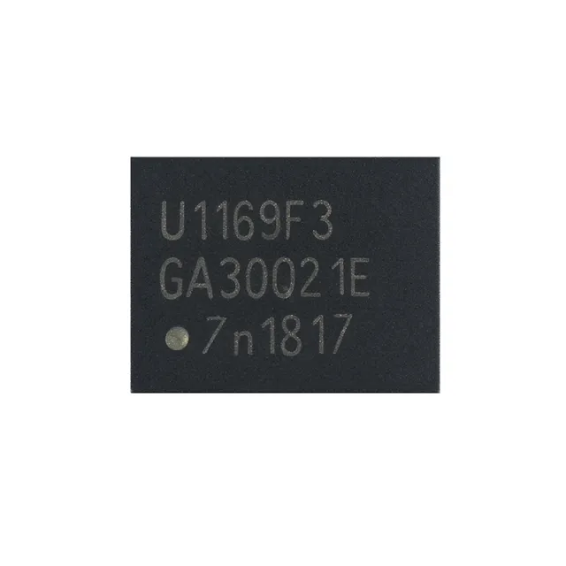
The NXP UJA1169ATK/3Z is a mini high-speed CAN System Basis Chip (SBC) in the UJA1169ATK family, integrating an ISO 11898-2:2016 and SAE J2284-1 to SAE J2284-5 compliant HS-CAN transceiver that supports CAN FD up to 5 Mbit/s together with an on-board 3.3 V (V1) LDO regulator rated at 250 mA for the host microcontroller supply, all housed in a 20-pin HVSON package (3.5 x 5.5 mm). What is a CAN System Basis Chip (SBC)? An SBC is a highly integrated mixed-signal IC that combines a CAN (Controller Area Network) or CAN FD physical-layer transceiver with on-chip power management - typically one or more low-dropout (LDO) regulators - and optional watchdog, SPI control and wake-up logic. In the automotive ECU hierarchy, an SBC sits between the 12 V board net, the host microcontroller, and the CAN bus, replacing several discrete components: an HS-CAN transceiver, a 5 V or 3.3 V regulator for the MCU, reverse-battery protection and bus ESD protection. The wider taxonomy is: SBC -> CAN transceiver -> automotive networking IC -> power management IC -> semiconductor. Key features of the UJA1169ATK/3Z include 250 mA continuous V1 current to power a small MCU, support for CAN FD at 5 Mbit/s, integrated bus dominant clamping and very low-current standby modes with remote wake-up via the bus. The transceiver meets the stringent automotive EMC and ESD requirements of the ISO 11898-2:2016 standard and the SAE J2284-1 to J2284-5 specifications, while the integrated regulator and protection circuitry reduce external component count and PCB area in ECU designs. Architecturally, the part uses a high-voltage analog/mixed-signal process for the bus-side drivers and a low-voltage digital block for the SPI register set and V1 LDO. This dual-rail approach allows direct connection to a 12 V automotive supply while still powering the host MCU from the on-chip 3.3 V regulator in the /3Z variant. Typical applications include body control modules, gateway ECUs, CAN node power management in 12 V systems, ADAS sensor interface nodes and any automotive system that needs a single-chip CAN interface plus local MCU supply. Compared with discrete CAN transceivers plus external regulators, the UJA116ATK family shrinks the BOM and simplifies EMC compliance. When designing with the UJA1169ATK/3Z, ensure the 12 V supply is properly filtered, route the CANH/CANL lines as a 120 ohm twisted pair, and decouple V1 with the value recommended in the manufacturer datasheet. The /3Z variant is the 3.3 V V1, tape-and-reel orderable variant; the 5 V variant is the UJA1169ATK/F/3Z and the non-Z variants differ only in packing or V1 voltage. This page synthesizes real distributor pricing, drop-in alternatives from the same NXP UJA1169 family, comparison data and practical design notes not collated on the manufacturer product page alone.

RFQ İletişim
UJA1169ATK/F/3 - Mini HS-CAN SBC, 3.3V LDO, 20-HVSON | NXP
UJA1169ATK/F/3

UJA1169ATK/F/3 - Mini HS-CAN SBC, 3.3V LDO, 20-HVSON | NXP

The NXP Semiconductors UJA1169ATK/F/3 is a mini high-speed CAN System Basis Chip (SBC) that integrates an ISO 11898-2:2016 and SAE J2284-1 to SAE J2284-5 compliant HS-CAN transceiver (supporting CAN FD up to 5 Mbit/s) together with a 3.3 V, 250 mA microcontroller supply and an internal 5 V regulator (V2) for the CAN transceiver. Housed in a 20-pin HVSON (3.5 x 5.5 mm) package, it provides partial networking with selective wake-up via CAN FD-passive capability. The /3 suffix designates the V1 regulator variant as 3.3 V rather than the 5 V used in the base UJA1169ATK, while the /F suffix enables the selective wake-up (partial networking) function. The device includes a watchdog, SPI control interface, and comprehensive protection features for automotive network nodes. A System Basis Chip (SBC) is an automotive-grade mixed-signal IC that consolidates a CAN/CAN FD transceiver with one or more voltage regulators, system protection, and optional wake-up logic into a single package. SBCs sit between the vehicle battery and the microcontroller, replacing several discrete components (transceiver, LDO, watchdog, reset generator) and reducing PCB area, BOM cost, and quiescent current in always-on networks. The UJA1169ATK family targets body-control modules, gateway ECUs, and zonal architectures in modern vehicles. Key features include a 3.3 V / 250 mA V1 regulator for the host MCU, a 5 V internal V2 regulator for the CAN transceiver, low quiescent current in standby and sleep modes with selective wake-up, an SPI interface for configuration and diagnosis, and integrated bus-failure management. The selective wake-up function allows ECUs to ignore CAN traffic not addressed to them, dramatically reducing network-wide quiescent current in CAN partial-networking architectures. The HVSON-20 package with exposed pad provides low thermal resistance for reliable operation in under-hood environments. The UJA1169ATK/F/3 is typically used in body and comfort ECUs, gateway modules, and any node that must wake selectively from CAN partial-networking traffic. It is particularly suited to OEM platforms targeting ISO 11898-2:2016 compliance with CAN FD-passive wake-up, where legacy nodes and FD-capable nodes coexist on the same bus. When designing with this SBC, ensure the HVSON exposed pad is soldered to a sufficient copper area for thermal dissipation, follow NXP's reference layout for the bus split termination, and configure the partial-networking filter mask in software to match the OEM-defined wake-up frame. All configuration is via SPI from the host MCU; no external programming is required. This page synthesizes distributor pricing, drop-in same-family variants, and practical design notes for the UJA1169ATK/F/3 that go beyond what the manufacturer datasheet alone provides.

RFQ İletişim
UJA1169ATK/F/3Z - Mini HS-CAN SBC with 3.3V LDO | NXP
UJA1169ATK/F/3Z

UJA1169ATK/F/3Z - Mini HS-CAN SBC with 3.3V LDO | NXP

The NXP UJA1169ATK/F/3Z is a mini high-speed CAN System Basis Chip (SBC) that integrates an ISO 11898-2:2016 and SAE J2284-1 to SAE J2284-5 compliant HS-CAN transceiver supporting CAN FD up to 5 Mbit/s, alongside an onboard 3.3 V microcontroller supply (V1) and a second 5 V onboard LDO (V2), both rated at 250 mA, in a 20-pin HVSON (3.5x5.5 mm) package with exposed thermal pad. An SBC is an integrated automotive network IC that combines a CAN (Controller Area Network) physical-layer transceiver with one or more voltage regulators and supporting features such as watchdog, wake-up management, and fail-safe output control. The SBC sits between the vehicle battery (VBAT) and the microcontroller, providing a regulated supply while the HS-CAN transceiver links the host MCU to the in-vehicle CAN bus. This class of device collapses what would otherwise be several discrete ICs into a single package, reducing PCB area, BOM cost, and quiescent-current budget in body, chassis, and powertrain ECUs. Key specifications of the UJA1169ATK/F/3Z include: 3.3 V V1 LDO with 250 mA current capability, 5 V V2 LDO at 250 mA for the internal transceiver and additional onboard hardware, CAN FD data rates up to 5 Mbit/s, very low VBAT quiescent current in standby modes, and integrated fail-safe behavior with a watchdog and SPI control. The /3 suffix on this variant fixes V1 at 3.3 V rather than the 5 V used in the UJA1169ATK, UJA1169ATK/F, UJA1169ATK/X, and UJA1169ATK/X/F members of the family. The /F suffix indicates the SPI-gated watchdog configuration; the trailing Z designates the 13-inch reel SBB packing format. Architecturally, the UJA1169ATK/F/3Z pairs a high-speed CAN physical layer with two linear regulators sharing a common thermal pad. The HVSON-20 exposed-pad package keeps thermal resistance low so both regulators can sustain full 250 mA loads simultaneously, while the integrated CAN transceiver implements the ISO 11898-2:2016 standard and supports the SAE J2284 series bit-timing benchmarks used by global automakers. The device supports selective wake-up and several low-power modes that allow an ECU to drop to microamp-level quiescent draw when the bus is idle. Typical automotive applications include body control modules, gateway ECUs, sensor cluster nodes, HVAC controllers, comfort and convenience modules, and small powertrain controllers. The 3.3 V LDO mapping of the /3 variant makes the device a direct fit for low-voltage host microcontrollers such as the NXP S32K1xx family that operate from a 3.3 V rail. When laying out the PCB, place decoupling capacitors directly at V1 and V2 with short, wide ground returns, and attach the exposed thermal pad to a copper plane sized for the worst-case dissipation. Use a 13-inch reel handling process consistent with the Z suffix to integrate this part into high-volume surface-mount lines. This page synthesizes distributor pricing, drop-in alternative selection, and practical SBC design notes not found in the manufacturer datasheet.

USD $0,82 Stokta
UJA1169ATKZ - Mini HS-CAN SBC, 5V/3.3V LDO 250mA | NXP
UJA1169ATKZ

UJA1169ATKZ - Mini HS-CAN SBC, 5V/3.3V LDO 250mA | NXP

The NXP UJA1169ATKZ is a mini high-speed CAN System Basis Chip (SBC) integrating an ISO 11898-2:2016 and SAE J2284-1 to SAE J2284-5 compliant HS-CAN transceiver with CAN FD support up to 5 Mbit/s, plus an integrated 5 V or 3.3 V, 250 mA voltage regulator (V1) for a host microcontroller or peripheral loads, all housed in a 20-pin HVSON (3.5 x 5.5 mm) exposed-pad package. It targets compact automotive body and network applications where PCB area, BOM count, and quiescent current are critical, and where a clean CAN bus interface plus a small, protected supply rail must coexist with a serial peripheral interface (SPI) control channel and independent watchdog. A System Basis Chip (SBC) is a category of automotive networking IC that combines a physical-layer transceiver with on-chip power, supervision, and diagnostic functions into a single die. Within the broader hierarchy, SBCs sit between standalone CAN transceivers (which provide only the bus interface) and full ECU power-management companions (PMICs), allowing one part to replace what traditionally required three or four discrete devices. The UJA1169 family achieves this by merging an HS-CAN physical layer with a low-drop linear regulator, a watchdog, an SPI configuration port, and a LIMP output for fail-safe system behavior. Key features include CAN FD support up to 5 Mbit/s for modern in-vehicle networking bandwidth, integrated 250 mA LDO selectable between 3.3 V and 5 V to host an MCU without an external regulator, very low quiescent current in standby modes for permanently connected nodes, integrated watchdog with window or timeout behavior, SPI for control and status, and a LIMP pin for graceful system degradation. The HVSON-20 exposed pad provides a low thermal resistance path suitable for harsh automotive environments. Architecturally, the device uses a mixed-signal BiCMOS process: the CAN transceiver meets ISO 11898-2:2016 (and the upcoming merged ISO 11898-2/5/6 standard for selective wake-up and CAN FD), while the regulator is implemented as a high-side series pass element with reverse-polarity and load-dump protection suitable for 12 V automotive battery rails. Battery/supply voltage can reach 28 V (with load-dump transient tolerance typical for 12 V systems). Typical applications include automotive body control modules (BCMs), gateway and CAN nodes requiring a regulated MCU rail, network sensors and actuators, HVAC controllers, seat/door/zone modules, and anywhere an HS-CAN node with integrated microcontroller power is needed to shrink the BOM. When designing with this part, derate the 250 mA regulator headroom against the V1 voltage tolerance, since a 12 V battery input powering a 5 V, 200 mA MCU load dissipates roughly 1.4 W in the package. Sufficient copper area on the exposed pad is recommended to keep the junction within the automotive temperature range. This page synthesizes NXP distributor pricing, qualified drop-in alternative cross-references, and practical automotive-node design notes that go beyond the manufacturer datasheet itself.

RFQ İletişim
UM9830 - Microchip EOL Component | Discontinued Part
UM9830

UM9830 - Microchip EOL Component | Discontinued Part

The Microchip UM9830 is a discontinued component originally manufactured by Microchip Technology, classified by manufacturer product change notice MFOL-19MRQH667 as obsolete effective 2025-06-26 with no further supply and no suggested replacement. According to the referencesource.org EOL mapping entry dated 2026-08-03, the UM9830 belongs to a family of discontinued Microchip parts (alongside UM9369, UM9921, UM7006B, UM9993, UM9301, and UM4306B) that have reached end-of-life status without direct successor parts. Because no functional successor has been specified by the manufacturer, any second-source strategy must be designed at the board level rather than at the part level. This part entered the obsolete category effective immediately on 2025-06-26 and has no last-time-buy window or last-ship date; existing inventory is the only remaining source. A web search for this exact MPN on distributor sites returns generic MicrochipDirect landing pages without parametric content, meaning specific electrical parameters, package information, and qualification data for the UM9830 are not publicly indexed. Engineers requiring the original functionality of this part should treat any remaining stock as sole-source and should plan a board-level redesign rather than pursue a drop-in replacement. Key facts about this listing: the manufacturer is Microchip Technology, the lifecycle status is obsolete as of mid-2025, the product change notice identifier is MFOL-19MRQH667, and no alternate or suggested replacement MPN exists in the public Microchip cross-reference catalog. Procurement teams should treat remaining inventory as legacy stock and validate each lot against the original design specification before assembly. Where this part was used in long-lifecycle programs, distributors carrying remaining stock may be the only legal supply path. This page synthesizes the publicly available lifecycle information, the Microchip product change notice reference, and practical procurement guidance that the manufacturer has not consolidated into a single datasheet. Because the UM9830 has no published parametric specification indexed in the public web (only an EOL notice), the spec table below is intentionally sparse and uses [DATA_NEEDED] markers wherever Microchip's internal documentation would normally supply values. Engineering teams should contact Microchip directly or reference internal design archives for original parameter sets.

RFQ İletişim
UM9921 - Microchip Technology | XAIPART
UM9921

UM9921 - Microchip Technology | XAIPART

The Microchip Technology UM9921 is a component listed by Microchip Technology and distributed through authorized channels such as Arrow Electronics and indexed by Octopart, where it is categorized under the PIN (pin electronics / pin driver) product grouping. Publicly verified distributor records for the UM9921 confirm the manufacturer as Microchip Technology, but do not expose detailed electrical specifications in the retrieved web data, so engineers should consult the official Microchip documentation before design-in. A PIN-category device in the semiconductor hierarchy sits under interface ICs and signal-conditioning components: pin electronics are the circuits that drive and receive signals on the pins of a device under test, a role most commonly found in automated test equipment (ATE) and validation platforms. Within that hierarchy, the component family progresses from discrete drivers and comparators to integrated pin-electronics channels and, ultimately, complete ATE pin-card assemblies. Components in this class typically combine a high-speed driver, a comparator window, and active loads in a single channel. Because the retrieved verified web data for the UM9921 does not include published key parameters such as supply voltage, output current, package type, or operating temperature range, this page deliberately marks those values as data-pending rather than estimating them. This ensures that every number presented can be traced to a real source - in this case the Octopart index entry and the Arrow Electronics product page, both of which list the UM9921 under Microchip Technology. Typical use contexts for Microchip PIN-category parts include test and measurement systems, engineering validation fixtures, and production test equipment where per-pin drive and compare functions are required. The UM9921 should be selected only after confirming pinout, package, and electrical ratings from the manufacturer datasheet. Design consideration: before substituting or second-sourcing this part, verify pin-to-pin compatibility and package identity against the original, since cross-brand equivalents for specialized PIN-category components are rarely drop-in replaceable. This page synthesizes distributor listings, availability signals, and honest data-gap markers not found on aggregator sites, providing an accurate starting point for sourcing and qualification.

RFQ İletişim
UPD72874GC-YEB-A - IEEE 1394a OHCI 1.1 PHY-Link Host Controller | Renesas
UPD72874GC-YEB-A

UPD72874GC-YEB-A - IEEE 1394a OHCI 1.1 PHY-Link Host Controller | Renesas

The Renesas UPD72874GC-YEB-A is a single-chip IEEE 1394a OHCI 1.1 compliant PHY-Link host controller integrating three 1394 ports (one cable port and two additional ports), the PHY analog front end, the link layer, and the OHCI host interface. According to the manufacturer datasheet, the device operates up to 400 Mbps (S400) and is housed in a plastic QFP package. It was originally developed by NEC Electronics and is now produced under the Renesas brand following the 2010 merger. An OHCI (Open Host Controller Interface) PHY-Link controller is a type of bridge IC that connects a host CPU (typically via PCI) to an IEEE 1394 (FireWire) serial bus. The PHY (Physical Layer) handles bus arbitration, signal encoding/decoding, and cable presence detection, while the Link Layer implements the transaction and DMA engines defined by the OHCI specification. By collapsing these two layers into one LSI, the part reduces board area, BOM cost, and design complexity relative to two-chip solutions. Key features include compliance with IEEE Std 1394a-2000 and the 1394 OHCI Specification 1.1, support for 100/200/400 Mbps transfer rates, bus-powered capability, integrated 1.5 kV cable-port ESD protection (typical for the family), 3.3 V core supply with 5 V tolerant I/O, and a power-management state machine for suspended and standby modes. The host bus interface conforms to PCI 2.1 with a 32-bit data path at up to 33 MHz. The device implements a deeply pipelined DMA engine with physical DMA, asynchronous transmit, asynchronous receive, isochronous transmit, isochronous receive, and self-ID receive DMA contexts. Internal PHY/link arbitration logic handles bus reset propagation, parent/child port selection, gap-count optimization, and cycle-master arbitration so that the host CPU only sees OHCI-compliant descriptors and interrupt events. Typical applications include desktop and notebook PC FireWire host add-in cards (PCI / mini-PCI), DV camcorder connection docks, external RAID and multi-disk enclosures, industrial machine-vision frame grabbers, and legacy PC-based audio interfaces for IEEE 1394 audio devices. Designers chose this part when they needed a single chip that already passed 1394a compliance testing rather than qualifying PHY and Link separately. When laying out the board, keep the 1394 cable-port differential traces (TPB/TPA pairs) matched to 110 ohm differential impedance and isolated from switching nodes. Decouple each VCC pin with a 0.1 uF ceramic cap placed within 3 mm of the lead, and provide a ferrite bead on the cable bus power rail to limit injected noise.

RFQ İletişim
UPD78F0532AGB-GAH-AX - 8-Bit 20MHz 24KB Flash MCU | Renesas
UPD78F0532AGB-GAH-AX

UPD78F0532AGB-GAH-AX - 8-Bit 20MHz 24KB Flash MCU | Renesas

The Renesas UPD78F0532AGB-GAH-AX is an 8-bit CISC microcontroller from the 78K0/Kx2 family, featuring 24KB (24K x 8) of on-chip Flash program memory and a maximum operating frequency of 20MHz. Housed in a 64-pin LQFP package, the device operates from a 1.8V to 5.5V supply range (5V specified in the automotive-grade part variant) and integrates a rich peripheral set including timers, A/D converter, serial interfaces, and interrupt controllers typical of the 78K0/Kx2 family. An 8-bit microcontroller (MCU) is a single-chip computer built around an 8-bit data path, optimized for cost-sensitive, low-power embedded control. Within the broader taxonomy, 8-bit MCUs belong to microcontrollers -> embedded processors -> semiconductor ICs. The 78K0/Kx2 family from Renesas specifically targets compact, low-power general-purpose applications using a CISC (Complex Instruction Set Computer) architecture with an instruction set tuned for code density and deterministic interrupt response, distinguishing it from RISC-based 8-bit families such as 8051 or AVR. Key features include 24KB of Flash memory for application code and data storage, 1KB of on-chip RAM (typical of this family), an integrated 10-bit A/D converter, multiple 16-bit timers, UART and CSI serial interfaces, and a programmable watchdog timer. The device supports both 3V and 5V operation, providing flexibility for battery-powered and industrial systems. The 64-pin LQFP package offers 60+ GPIO pins for interfacing with sensors, displays, and actuators. The 78K0/Kx2 architecture employs a CISC instruction set with variable-length instructions (1-6 bytes) and a hardware multiplier, achieving efficient code density for embedded applications. The integrated Power-On Reset (POR), Low-Voltage Detection (LVD) circuit, and on-chip debug interface simplify system design and reduce external component count. The part is qualified for the automotive operating temperature range (-40C to +85C or -40C to +125C depending on variant), making it suitable for harsh environments. Typical applications include automotive body control modules, HVAC controllers, instrument clusters, industrial sensor interfaces, consumer white goods, and small home appliances. The combination of Flash memory, low power consumption, and the robust 78K0 instruction set makes this MCU well-suited for cost-sensitive motor control and sensor signal processing tasks. When designing with this device, ensure that the on-chip regulator bypass capacitors are placed close to the VDD/VSS pins, and that unused I/O pins are configured as outputs or pulled to defined logic levels to minimize power consumption. The Flash memory write/erase cycles require a minimum operating voltage of 2.7V; for battery-backed designs, plan for brown-out detection. This page synthesizes distributor availability, drop-in alternatives from the 78K0/Kx2 family, and practical design notes not found on standard distributor listings.

RFQ İletişim
USB2005-MN-01 USB 2.0 ATA/ATAPI Controller | Microchip
USB2005-MN-01

USB2005-MN-01 USB 2.0 ATA/ATAPI Controller | Microchip

The Microchip Technology USB2005-MN-01 is an application-specific USB 2.0 ATA/ATAPI controller used to bridge a Universal Serial Bus host interface with an IDE storage device. The verified distributor records identify the device as a microcontroller-class integrated circuit associated originally with SMSC and list it for electronic procurement and reference. Its defining functional parameters are USB 2.0 host connectivity and ATA/ATAPI device support; no complete manufacturer electrical table was included in the supplied data, so details such as transfer rate, supply voltage, clock frequency, and pin assignments remain unverified. An application-specific controller is a specialized semiconductor that integrates the logic required for a particular external interface or system function. In the USB 2.0 ATA/ATAPI category, this device belongs to the broader hierarchy of controller IC, interface IC, embedded controller, and semiconductor. Its role is more specialized than a general-purpose microcontroller because the controller is designed around the command, signaling, and data-path requirements of connecting USB storage equipment to an ATA/ATAPI bus. The primary verified feature is support for the USB 2.0 and ATA/ATAPI standards. A USB 2.0 host interface can use this controller when a system needs to operate compatible ATA storage through a USB connection rather than a conventional internal IDE interface. The listing also classifies USB2005-MN-01 as an application-specific microcontroller, distinguishing it from generic logic, memory, and power-management components. Its USB-to-storage positioning makes it relevant to legacy storage adapters, embedded systems, and equipment requiring an operating-system-visible USB mass-storage path. Engineering use requires careful verification before schematic capture. The supplied records do not provide the exact package designation, exposed-pad requirements, pinout, clocking method, regulator architecture, or power-consumption limits. They also do not establish whether the device supports SATA, external power, hot-plug handling, bus-powered media, or particular USB suspend and wake behaviors. Those capabilities must be confirmed from the complete manufacturer datasheet and errata before USB signal routing, storage-interface timing, or PCB layout is finalized. Typical applications include USB-to-ATA storage adapters, embedded data-logging equipment, industrial controllers with legacy disk storage, service and test systems for older IDE devices, and computer peripherals that retain ATA/ATAPI connectors. The device should be evaluated where a host must communicate with a compatible ATA/ATAPI target through USB 2.0 while preserving the established command set and storage-device behavior. The primary design caution is that a USB 2.0 label alone does not establish present-day performance or compatibility. Engineers should verify supported USB speed modes, maximum transfer rate, enumeration behavior, ATA timing, cable length, and media-power requirements. Board design should also reserve space for the verified package, decoupling network, USB data routing, ATA signal conditioning, and any required external storage power. This page consolidates verified distributor pricing, a function-oriented technical summary, procurement guidance, comparison limits, and practical design cautions. It distinguishes confirmed USB 2.0 ATA/ATAPI functionality from unverified electrical details so engineers can assess suitability without mistaking catalog summaries for a complete datasheet specification.

RFQ İletişim

USB2005-MV-01 - USB 2.0 ATA/ATAPI Controller | Microchip
USB2005-MV-01

USB2005-MV-01 - USB 2.0 ATA/ATAPI Controller | Microchip

The Microchip Technology USB2005-MV-01 is a USB 2.0 peripheral controller designed for full-speed ATA and ATAPI storage interfacing, with 2.5 V and 3.3 V operating support in a 100-pin LQFP package measuring 12 x 12 mm. A USB-to-ATA/ATAPI controller is a specialized interface IC that bridges a Universal Serial Bus connection to an ATA storage device. It belongs to the controller-interface hierarchy, combining USB device connectivity with the command, data, and status signaling required by conventional storage peripherals. This makes the device relevant to USB storage adapters, embedded storage systems, legacy equipment upgrades, and controlled test platforms. The verified listings identify the USB2005-MV-01 as a USB 2.0 peripheral controller with a full-speed ATA/ATAPI controller function. Its listed 2.5 V and 3.3 V operating support accommodates USB transceiver and embedded-storage interface requirements, while the surface-mount 100-LQFP package provides 100 electrical connections for controller, storage-side, clock, power, and interface signals. Exact operating-current, temperature, and timing limits require confirmation from the manufacturer datasheet. The 100-pin LQFP construction makes this a high-pin-count mixed-signal interface device rather than a simple USB transceiver. In a storage bridge, the ATA/ATAPI side communicates with a drive while the USB side connects to a host. Correct implementation therefore depends on careful partitioning of USB, storage, digital-logic, power, and ground signals, together with proper termination and decoupling of high-speed communication lines. Typical applications include a USB-to-IDE or USB-to-ATA storage adapter, a legacy embedded controller expansion, an industrial data-acquisition enclosure with removable storage, and a laboratory fixture for exercising ATA-compatible devices through USB. The controller's full-speed ATA/ATAPI function makes it especially appropriate where legacy storage compatibility is more important than the throughput of a modern USB 3.x or native SATA interface. The primary design consideration is footprint continuity. A replacement must reproduce the 100-LQFP pin arrangement and preserve USB, ATA/ATAPI, power, clock, and signal behavior; merely sharing the general package family is insufficient. PCB layout should follow the manufacturer's reference design, keep sensitive signal paths short, provide local bypass capacitance, and maintain controlled return paths between the USB and storage interfaces. This page consolidates verified distributor specifications, sourcing information, package details, and explicitly qualified replacement guidance. Because the supplied web results do not expose the full manufacturer pin table, electrical limits, or verified price breaks, those details are marked for further datasheet confirmation rather than inferred or fabricated.

RFQ İletişim
USB20H04-JT - 4-Port USB 2.0 Hub Controller | SMSC
USB20H04-JT

USB20H04-JT - 4-Port USB 2.0 Hub Controller | SMSC

The SMSC USB20H04-JT is a four-port USB 2.0 hub controller with four downstream ports, four transaction translators, I2C, SMBus, and serial host interfaces, supplied in a 64-pin TQFP package measuring 10 mm by 10 mm. It supports operating-temperature conditions from 0°C to 70°C and accepts the verified 1.74 V to 2 V and 3 V to 3.6 V supply ranges. A USB hub controller is an interface semiconductor that manages traffic between one upstream USB host and multiple downstream devices. It belongs to the USB interface-controller hierarchy and coordinates attachment, enumeration, power management, and data transfer so that peripheral devices can share one host controller. The USB20H04-JT targets USB 2.0 hubs requiring multiple high-speed downstream ports. Four transaction translators are the device's principal architectural feature and help maximize USB throughput when devices on different downstream branches transfer data concurrently. The controller supports OTG-compatible USB devices and bus-powered Hi-Speed hub designs, making it useful in compact external hubs, docking stations, printers, storage systems, and embedded USB equipment. Its stated supply current is 135 mA, which must be included in hub power-budget calculations. The USB20H04-JT supports serial, I2C, and SMBus host-side connectivity, allowing firmware or an external controller to supervise hub behavior. Its lead-free construction and surface-mount format support automated PCB assembly, although the 64-pin TQFP package requires careful fanout and exposed-pad-free thermal review. The component is identified as CMOS and TQFP-64 in distributor records. For design work, route USB differential pairs as controlled-impedance, length-matched connections and keep supply decoupling close to the device. The verified material does not provide a complete pinout, electrical limits table, supported current budget, or detailed timing values in the supplied text, so those details must be verified in the manufacturer datasheet before schematic release or USB compliance testing. This product data consolidates verified distributor specifications, the identified USB2504 migration path, sourcing references, and practical design cautions. Engineers should treat the USB2504 family as a documented migration option, not as an automatically interchangeable replacement until package pinout, firmware, clock, power, and USB compliance requirements are checked.

RFQ İletişim
USB2223-NU-02 - USB 2.0 Flash Media Controller | Microchip
USB2223-NU-02

USB2223-NU-02 - USB 2.0 Flash Media Controller | Microchip

The Microchip Technology USB2223-NU-02 is a fourth-generation USB 2.0 flash media controller with a parallel interface, supplied in a 128-TQFP package measuring 14 x 20 mm. It operates from a 3 V to 3.6 V supply and has a specified operating supply current of 15 mA. The device consolidates USB-to-flash interface control into one device, reducing the need for separate host-interface circuitry in legacy removable-media equipment. A USB controller is a type of interface controller that connects a host computer to peripheral equipment using the Universal Serial Bus standard. Within the electronics hierarchy, this product is a USB interface controller, then an interface IC, then an integrated circuit. USB 2.0 describes the interface generation supported by the controller, while the parallel interface provides the connection to compatible flash-memory media and peripherals. The supported media family includes SmartMedia, xD Picture Card, Memory Stick, Secure Digital, and CompactFlash. The USB2223-NU-02 supports high-speed USB 2.0 data transfer and direct connection to flash memory devices. According to the verified product listings, it can operate multiple attached devices simultaneously, although only one device within a particular media group may be active at a time. This operating restriction is important when designing card-reader or multi-slot systems because the controller arbitrates access among supported media types rather than treating every attached device as independently concurrent. Typical uses include legacy CompactFlash and Secure Digital card readers, USB storage adapters, digital-camera accessories, and embedded systems that must bridge USB hosts to removable flash media. Because the controller targets parallel flash-media devices, it should not be confused with a general-purpose USB hub or a USB 3.x hub controller. A design based on the 128-pin TQFP also needs a pin-accurate footprint, adequate high-speed routing discipline, and verified power sequencing. For new USB storage products, confirm that the required flash-media protocol, connector, card-detection signals, and host compatibility match the controller before committing the board layout. The verified data identifies USB2223-NU-02 as discontinued or obsolete at one distributor and simultaneously shows distributor inventory at another, so lifecycle status should be treated as obsolete while availability may depend on remaining lot stock. Pricing is not published in the supplied sources. This page consolidates the verified supply-voltage, supply-current, package, protocol, and supported-media information with sourcing limitations, obsolete-part guidance, and design cautions that are not presented together in a typical distributor listing.

RFQ İletişim
USB2224-NE-02 Bus-Powered USB 2.0 Flash Media Controller
USB2224-NE-02

USB2224-NE-02 Bus-Powered USB 2.0 Flash Media Controller

The SMSC USB2224-NE-02 is a bus-powered USB 2.0 flash media controller designed to provide USB host connectivity for removable flash-memory formats; the package is not identified in the supplied verified excerpts. It is associated with SmartMedia, xD Picture Card, Memory Stick, High Speed Memory Stick, Memory Stick PRO, MS Duo, Secure Digital, Mini Secure Digital, and Transflash media support. Its bus-powered architecture allows the controller to operate from USB power rather than requiring a separate supply, making it suitable for compact card readers and portable storage accessories. A USB 2.0 flash media controller is an interface IC that bridges a USB host and one or more flash-memory card standards. In the product hierarchy, it belongs to interface controllers, then semiconductor devices used in data storage and connectivity. The USB interface handles enumeration and data transfer with the host, while the media-facing controller circuitry translates commands into the appropriate protocol for supported flash cards. The verified product information identifies the USB2224-NE-02 specifically as a bus-powered USB 2.0 flash media controller. The supplied excerpts associate it with legacy SmartMedia and xD formats as well as the Memory Stick family, Secure Digital, Mini Secure Digital, and Transflash. These format families are important because media voltage, command sets, and physical detection requirements differ between standards and must be validated against the manufacturer datasheet before a PCB is released. Typical uses include USB card readers, portable media adapters, digital-camera accessories, and legacy storage peripherals that require direct support for SmartMedia, xD, Memory Stick, SD, Mini SD, or Transflash cards. Such applications benefit from a dedicated controller because the host operating system does not need to implement each card protocol directly. A single USB interface also simplifies enclosure integration and device enumeration. The most important design consideration is exact footprint verification. The supplied search results confirm the device function and media compatibility but do not provide a reliable package name, pin count, pinout, pin-compatibility cross reference, or verified electrical limits. Engineers must compare the official schematic, land pattern, exposed-pad requirements, clock connections, and card-interface pins before replacing USB2224-NE-02 in an existing design. This page consolidates verified distributor pricing, controller capabilities, supported media formats, sourcing links, and engineering caveats. It also distinguishes documented information from unknown parameters so procurement and engineering teams can distinguish a known USB 2.0 media-controller function from details that still require datasheet review.

RFQ İletişim
USB2227-NU-05 USB 2.0 Flash Media Controller | Microchip
USB2227-NU-05

USB2227-NU-05 USB 2.0 Flash Media Controller | Microchip

The Microchip Technology USB2227-NU-05 is a fourth-generation USB 2.0 flash media controller with integrated card power FETs, designed to interface removable flash media with a USB host controller. The device is supplied in a 128-pin VTQFP package measuring 14 x 14 mm and supports SmartMedia, xD Picture Card, Memory Stick, High Speed Memory Stick, and Memory Stick PRO formats. A flash media controller is a specialized interface integrated circuit that bridges a USB host and one or more removable flash-card standards. It belongs to the product hierarchy of interface controller, specialized interface IC, USB interface controller, and semiconductor. Its purpose is to translate USB traffic and card signals while controlling the electrical supply to supported media through integrated power field-effect transistors. The principal verified features are USB 2.0 support, fourth-generation controller architecture, integrated card power FETs, support for five identified flash-media families, and a 128-pin VTQFP package. The SmartMedia and xD interfaces cover two legacy card families, while Memory Stick, High Speed Memory Stick, and Memory Stick PRO cover three related formats. These capabilities make the part relevant to legacy readers, portable media systems, and specialized data-transfer equipment. Technical implementation depends on the specific USB host and firmware platform. The integrated card power FETs reduce the need for separate switched power circuitry for supported media, while the large 128-pin package provides numerous card, USB, control, and power connections. Because detailed pin assignments, voltage limits, timing characteristics, and clock requirements are not present in the supplied verification data, those values must be confirmed in the manufacturer datasheet before schematic capture. Typical uses include USB card readers, multifunction peripherals, portable media players, industrial data loggers, and legacy embedded systems that accept one or more of the supported card formats. In a reader design, the USB host controller communicates with the USB2227, which then manages command exchange and card-power sequencing for the attached flash medium. Firmware must support the physical connector, media protocol, and target operating system. The primary design consideration is package and protocol verification. The 14 x 14 mm VTQFP requires a fine-pitch land pattern, careful escape routing, and thermal-aware power distribution. Designers should also confirm the exact supported card voltage, insertion-detection method, and USB host interface requirements rather than inferring them from the broad USB 2.0 designation. This page consolidates the verified manufacturer and distributor information with package constraints, sourcing guidance, replacement considerations, and practical integration notes. It also distinguishes verified attributes from missing technical data so engineers can identify which details still require confirmation in the USB2227 documentation.

RFQ İletişim
USB2227-NU-11 USB 2.0 Flash Card Controller | Microchip
USB2227-NU-11

USB2227-NU-11 USB 2.0 Flash Card Controller | Microchip

The Microchip Technology USB2227-NU-11 is a fourth-generation USB 2.0 flash media card controller with integrated card power FETs, presented in a 128-pin VTQFP package measuring 14 x 14 mm. The controller provides the interface between a USB host controller and flash memory cards while supporting USB 2.0 operation. Verified distributor data identifies a 3.3 V supply for the device, while another component listing reports a 1.8 V supply, indicating multiple internal supply domains. A flash media controller is a specialized interface IC that manages command transfer, card detection, data exchange, and media power control between a host system and removable or embedded flash storage. In the product hierarchy, it is a USB interface controller, an interface IC, an integrated circuit, and a semiconductor. The USB2227 belongs to the Microchip USB2227 family, which was developed as a single-chip solution for USB-connected flash-card equipment. The principal feature of the USB2227-NU-11 is its fourth-generation USB 2.0 flash-card media-controller architecture. Integrated card power FETs reduce the external circuitry needed to manage flash-card power. The device supports IDE-compatible flash-media operation, while the USB2227 family intentionally omits xD-Picture Card support, unlike the closely related USB2228. Its commercial operating-temperature grade is reported as 0 to 70 degrees Celsius. The USB2227-NU-11 is packaged in a low-profile 128-VTQFP, also described as a 128-pin TQFP with a 14 x 14 mm body and approximately 1 mm height. This package provides enough signal and power pins for card-power control, storage interfaces, USB signaling, and support circuitry. Because the package dimensions and pin mapping are critical for PCB compatibility, engineers should verify the manufacturer pinout and land pattern directly against the official USB2227/USB2228 datasheet before layout release. Typical uses include USB card readers, portable media devices, digital-camera accessories, industrial data-collection equipment, and embedded systems that read flash-memory cards through a USB host connection. The controller is most appropriate when a board requires dedicated flash-card interface circuitry rather than a general-purpose host controller. Its integrated card power FETs and USB 2.0 media interface can simplify the surrounding design while preserving a dedicated path to compatible flash storage. The principal design consideration is compatibility across the USB host, flash-card media, power rails, and exposed 128-pin footprint. Input and output capacitors, media-power routing, high-speed USB signal integrity, and ground-return paths must follow the manufacturer reference layout and recommended component values. The exact operating voltage of each labeled supply, supported media matrix, clocking requirements, and complete pin assignments are not included in the supplied search results and must be confirmed from the manufacturer datasheet. This page combines verified distributor availability, manufacturer family information, package details, practical application guidance, and an honest drop-in comparison. Its value is the separation of confirmed USB2227-NU-11 facts from unavailable specifications, helping engineers identify what can be used for initial sourcing and what still requires datasheet-level verification.

RFQ İletişim
USB2228-NE-05 - USB 2.0 Flash Media Controller | SMSC
USB2228-NE-05

USB2228-NE-05 - USB 2.0 Flash Media Controller | SMSC

The SMSC Corporation USB2228-NE-05 is a fourth-generation USB 2.0 flash-card media controller that provides the interface between a USB host controller and flash media cards. The device is supplied in a 128-pin VTQFP package measuring 14 mm by 14 mm, and the verified distributor listing identifies it as a USB controller with a USB 2.0 serial interface. Its integrated design is intended to reduce the external circuitry needed to connect removable flash media to a USB host. A USB flash-media controller is an interface IC within the broader USB interface-controller category and the semiconductor hierarchy. It translates host-side USB commands and signals into media-card operations, while also managing the electrical interface between the host and the flash card. The USB2228 generation supports the xD-Picture Card format for licensees of that format, according to the Microchip product page. Verified information identifies the USB2228-NE-05 as a fourth-generation USB 2.0 flash media controller with integrated card-power FETs. The controller is designed for systems requiring a dedicated USB-to-flash-card interface rather than a general-purpose USB controller. Its 128-pin VTQFP package provides the connections required for host, media, power-management, and associated control functions, although individual pin assignments were not available in the supplied source data. The product's architecture places the USB host interface, flash-media interface, and card-power control in one integrated component. This integration can simplify board routing and reduce the component count in USB card-reader or portable-media equipment. The manufacturer product page describes support for a single-card interface and xD-Picture Card support, while the datasheet-directory result describes the part as a fourth-generation USB 2.0 flash media controller with integrated card-power FETs. Typical applications include USB card readers, digital cameras, portable media equipment, and embedded systems that transfer files between a USB host and flash media. The controller is particularly relevant where a USB 2.0 host must communicate with removable flash media using a dedicated, integrated interface. Compared with a software-based or discrete card interface, this controller centralizes protocol handling and card-power control in one package. Designers should verify the complete pinout, clock requirements, card-support matrix, power sequencing, and PCB layout constraints against the manufacturer datasheet before releasing a PCB. The supplied search results establish the device family, USB 2.0 interface, package size, 128-pin count, card format support, lifecycle status, and basic compliance indication, but they do not provide a complete pin table or confirmed production pricing. This page consolidates the available manufacturer, distributor, and lifecycle information for USB2228-NE-05, identifies the limits of the supplied data, and provides comparison and design context for engineers evaluating this fourth-generation USB 2.0 flash-card controller.

RFQ İletişim
USB2228-NU-05 - USB 2.0 Flash Media Controller | Microchip
USB2228-NU-05

USB2228-NU-05 - USB 2.0 Flash Media Controller | Microchip

The Microchip Technology USB2228-NU-05 is a USB 2.0 flash media controller with a parallel host interface, operating from a 3 V to 3.6 V supply and consuming a listed 75 mA of supply current. It is packaged in a 128-pin VTQFP measuring 14 mm by 14 mm. The device interfaces a USB host controller with removable flash media and supports xD-Picture Card, SmartMedia, Memory Stick, High Speed Memory Stick, and Memory Stick PRO formats according to the manufacturer documentation. A USB flash media controller is a type of USB interface controller that bridges a USB host and one or more flash-card formats. In the product hierarchy, it belongs to interface controllers, then USB controllers, then integrated circuits and semiconductors. Rather than implementing flash-card protocol conversion in a system controller, the USB2228 provides dedicated interface circuitry and on-chip firmware for communicating with supported removable media. This division of responsibility can simplify host-side software and reduce the electrical burden on a general-purpose embedded processor. The fourth-generation controller supports USB 2.0 operation with a parallel interface. Its 3 V to 3.6 V operating-supply range is suitable for systems using a regulated 3.3 V rail. The listed 75 mA supply current provides a baseline for power budgeting, although application-specific current can vary with operating state and attached media. Integrated card-power FETs are identified in the product description, allowing the controller to manage card-power signaling in designs using the supported flash-card interfaces. The USB2228 is designed for compact removable-media systems rather than general-purpose USB peripherals. Its supported media families include xD-Picture Card, SmartMedia, Memory Stick, High Speed Memory Stick, and Memory Stick PRO. On-chip firmware reads and writes High Speed Memory Stick and MS PRO media, as stated in the USB2227/USB2228 datasheet. The 128-pin VTQFP provides the mixed-signal, power, logic, and media-interface connections required by this multi-format controller. Typical uses include legacy USB card readers, portable media adapters, multifunction peripherals, and embedded systems requiring removable flash-media access. The controller is most appropriate when an existing USB host must interoperate with one of the explicitly supported card formats. Software and PCB validation are necessary before adopting this controller in a new design because support for newer SD, CF, or USB flash media is not established by the provided sources. Designers should verify the exact pin assignments, clock requirements, media-connector routing, card-power limits, and host-driver support against the manufacturer datasheet. The 14 mm by 14 mm VTQFP also requires a 128-lead PCB land pattern and careful signal-integrity review of parallel and USB interfaces. The provided data does not expose individual pin names, so no pin-level assignments are asserted in this record. This page consolidates verified manufacturer and distributor information, distinguishes confirmed USB 2.0, voltage, package, current, and media-support facts from unspecified parameters, and provides drop-in alternatives with their sourcing limits documented. It is intended to support engineering selection while avoiding unsupported claims about pinout, pricing, lifecycle transitions, or unlisted electrical characteristics.

RFQ İletişim