Ürünler (35.000+)

XC7VX690T-2FFG1927I - Virtex-7 XT FPGA 693K Logic Cells | AMD
XC7VX690T-2FFG1927I

XC7VX690T-2FFG1927I - Virtex-7 XT FPGA 693K Logic Cells | AMD

The AMD XC7VX690T-2FFG1927I is a high-performance Virtex-7 XT Field Programmable Gate Array (FPGA) from the 7 series family, designed for ultra high-end connectivity bandwidth, logic capacity, and signal processing capability. It features 693,120 logic cells, 54,190,080 block RAM bits, and 600 user I/Os, packaged in a 1924-ball FCBGA (FFG1927) with an industrial temperature range (-40°C to +100°C). The device operates with a core supply voltage of 1.0V and supports high-speed serial transceivers, making it ideal for demanding applications such as data center acceleration, aerospace and defense, and high-performance computing. A Field Programmable Gate Array (FPGA) is an integrated circuit that can be configured by the customer after manufacturing to implement any digital logic function. FPGAs consist of programmable logic blocks, configurable interconnects, and I/O blocks, allowing designers to create custom hardware accelerators, protocol bridges, and complex digital systems. The Virtex-7 XT family is the highest-performance segment of the 7 series, offering the largest logic density and the most advanced features, including integrated DSP slices, block RAM, and high-speed transceivers. Key features of the XC7VX690T-2FFG1927I include 3,600 DSP slices for high-throughput signal processing, 54,190,080 bits of block RAM for on-chip data storage, and 600 user I/Os supporting various I/O standards. The device also includes 80 GTX transceivers capable of up to 12.5 Gbps, providing high-speed serial connectivity for PCIe, Ethernet, and other protocols. The -2 speed grade offers a balance between performance and power consumption, while the industrial temperature grade ensures reliable operation in harsh environments. Architecturally, the Virtex-7 XT FPGA is built on a 28nm high-k metal gate (HKMG) process technology, delivering high performance with lower power compared to previous generations. The device includes advanced clock management tiles (CMTs) with MMCM and PLL for precise clock generation, and supports partial reconfiguration for dynamic logic updates. The configurable logic blocks (CLBs) provide flexible logic implementation, and the integrated block RAM can be configured in various aspect ratios for efficient data storage. Typical applications include high-performance computing acceleration, radar and signal intelligence systems, medical imaging, and wired communications infrastructure. The high transceiver count and logic density make it suitable for implementing complex algorithms and high-bandwidth data paths. The industrial temperature range allows deployment in outdoor and automotive environments where temperature extremes are common. When designing with this FPGA, careful attention must be paid to power supply decoupling and thermal management. The device requires multiple supply rails (VCCINT, VCCAUX, VCCO) with proper sequencing, and the high power dissipation necessitates a heatsink or active cooling for sustained operation. Refer to the Virtex-7 FPGA data sheet and PCB design guidelines for detailed recommendations.

RFQ İletişim
XC7VX690T-2FFG1930I - Virtex-7 XT FPGA 693K Logic Cells | AMD
XC7VX690T-2FFG1930I

XC7VX690T-2FFG1930I - Virtex-7 XT FPGA 693K Logic Cells | AMD

The AMD XC7VX690T-2FFG1930I is a high-performance Virtex-7 XT Field Programmable Gate Array (FPGA) fabricated on a 28nm process technology. It delivers 693,120 logic cells, 1,000 user I/O pins, and 54,190,080 block RAM bits, all housed in a 1924-ball FCBGA (FFG1930) package. This device is engineered for demanding applications requiring massive parallel processing, high-speed serial transceivers, and extensive logic resources. An FPGA (Field Programmable Gate Array) is an integrated circuit that can be configured by the customer or designer after manufacturing. Unlike fixed-function ASICs, FPGAs contain an array of programmable logic blocks, interconnects, and I/O blocks that can be programmed to implement any digital logic function. The Virtex-7 XT family sits at the high end of AMD's 7-series FPGA portfolio, positioned above the Artix and Kintex families, offering the highest logic density and transceiver count for system-level integration. Key features of the XC7VX690T-2FFG1930I include 693,120 logic cells, 1,000 user I/O pins, 54,190,080 bits of block RAM, and 80 GTX transceivers supporting data rates up to 12.5 Gbps. The -2 speed grade provides a balanced performance point, while the industrial temperature grade (-I) supports operation from -40°C to +100°C. The device operates from a 1.0V core voltage and is available in a 1924-ball FCBGA package with 1.0mm ball pitch. Architecturally, the Virtex-7 XT integrates advanced clock management tiles (CMTs), DSP48E1 slices for high-throughput digital signal processing, and PCIe hard blocks for system connectivity. The 28nm HPL (High-Performance Low-Power) process technology balances speed and power efficiency, making it suitable for both compute-intensive and power-sensitive designs. The device supports partial reconfiguration, allowing dynamic updates to logic functions without powering down the system. Typical applications include high-end wired communications (100G/400G line cards), data center acceleration, radar and electronic warfare systems, medical imaging, and broadcast video processing. The combination of high logic density, transceiver count, and I/O flexibility makes it ideal for ASIC prototyping and complex system-on-chip designs. When designing with this device, careful attention must be paid to power supply decoupling, with multiple 1.0V core rails and 1.8V auxiliary rails requiring proper filtering. The FCBGA package demands a multi-layer PCB with controlled impedance routing for high-speed transceivers and adequate thermal management for high-power operation.

RFQ İletişim
XC7Z010-1CL225I - 667MHz Dual Cortex-A9 SoC | AMD
XC7Z010-1CL225I

XC7Z010-1CL225I - 667MHz Dual Cortex-A9 SoC | AMD

The AMD XC7Z010-1CL225I is a Zynq-7000 adaptive SoC combining a dual-core ARM Cortex-A9 MPCore processor with an Artix-7 FPGA fabric in a 225-CSPBGA package. The device provides 28,000 logic cells, a stated operating frequency of 667 MHz, and an industrial temperature range of -40°C to +100°C. Its programmable logic and integrated processing system make it suitable for embedded control, industrial automation, communications, image processing, and compact edge systems. A Zynq-7000 SoC is a heterogeneous system-on-chip, combining an ARM microprocessor subsystem and programmable FPGA logic in one package. This integration reduces component count and allows software running on the Cortex-A9 processors to exchange data directly with hardware implemented in the FPGA fabric. The result is a flexible platform for systems that need deterministic parallel processing alongside a conventional embedded software environment. The XC7Z010-1CL225I provides two ARM Cortex-A9 cores, 28K FPGA logic cells, and a 667 MHz processor frequency. Its 225-CSPBGA package measures 13 mm by 13 mm according to distributor product data. The device operates from a nominal 1 V supply, with a stated minimum of 0.95 V and maximum of 1.05 V, and is identified as RoHS compliant. These characteristics position it as an entry-level Zynq device for designs requiring more parallelism than a conventional microcontroller provides. The architecture allows designers to partition a design between software and programmable logic. Software can manage operating-system tasks, control flow, and external interfaces, while the FPGA fabric can implement parallel data paths, custom interfaces, signal processing, or timing-critical functions. The available data identifies this device as a Zynq-7000 SoC with an Artix-7 FPGA fabric, but detailed block counts, memory interfaces, I/O counts, and power characteristics require confirmation from the AMD device documentation. Typical applications include industrial automation controllers, networked embedded gateways, motor and motion-control systems, communications equipment, sensor-processing platforms, and cost-sensitive FPGA-assisted processors. The dual Cortex-A9 configuration supports concurrent software workloads, while the FPGA fabric can accelerate operations that would otherwise burden the processor or require separate programmable logic. When designing a board around the XC7Z010-1CL225I, engineers must follow the AMD Zynq-7000 package pinout and power-sequencing guidance. The BGA footprint requires appropriate PCB layout, thermal analysis, and assembly process controls. Because the available distributor snippet provides limited electrical detail, final power budgeting, decoupling, DDR memory connectivity, and I/O standards must be verified against the official manufacturer documentation before release.

RFQ İletişim
XC7Z010-1CLG225I - Zynq-7000 SoC, 667MHz, 28K Logic Cells | AMD
XC7Z010-1CLG225I

XC7Z010-1CLG225I - Zynq-7000 SoC, 667MHz, 28K Logic Cells | AMD

The AMD XC7Z010-1CLG225I is a Zynq-7000 SoC integrating a dual-core ARM Cortex-A9 MPCore processor with an Artix-7 FPGA fabric in a 225-ball CSPBGA (13x13 mm) package. It operates at a maximum processor frequency of 667 MHz and provides 28K logic cells, making it a versatile platform for embedded systems requiring both software programmability and hardware acceleration. A System-on-Chip (SoC) combines a processor (CPU) with other system components such as memory controllers, peripherals, and programmable logic on a single die. The Zynq-7000 family specifically merges a hard ARM processing system (PS) with a programmable FPGA fabric (PL), enabling designers to implement custom hardware accelerators alongside software applications. This architecture bridges the gap between traditional microcontrollers and FPGAs, offering the flexibility of programmable logic with the ease of software development. Key features include dual ARM Cortex-A9 cores with NEON and CoreSight debug, 28K Artix-7 logic cells, 667 MHz maximum frequency, and industrial temperature range (-40°C to +100°C). The device supports a nominal supply voltage of 1.0V (0.95V to 1.05V) and includes integrated memory controllers, DMA, and a rich set of peripherals. The CLG225 package provides a compact footprint suitable for space-constrained designs. The Zynq-7000 architecture separates the PS and PL, allowing independent clocking and power management. The PS includes a DDR3/DDR3L memory controller, Gigabit Ethernet, USB 2.0, and SDIO interfaces, while the PL provides configurable logic, DSP slices, and block RAM. This separation enables optimized performance and power efficiency for heterogeneous workloads. Typical applications include industrial motor control, software-defined radio, medical imaging, and automotive driver assistance systems. The combination of ARM processing and FPGA fabric makes it ideal for real-time control, signal processing, and protocol bridging. The industrial temperature grade ensures reliable operation in harsh environments. When designing with this device, careful attention must be paid to power supply sequencing and decoupling. The multiple power rails (VCCINT, VCCAUX, VCCO) require proper filtering and sequencing to ensure reliable startup and operation. Refer to the Zynq-7000 TRM (UG585) for detailed power-up requirements.

RFQ İletişim
XC7Z010-1CLG400C - 667MHz Zynq SoC, 28K Logic | AMD
XC7Z010-1CLG400C

XC7Z010-1CLG400C - 667MHz Zynq SoC, 28K Logic | AMD

The AMD XC7Z010-1CLG400C is a Zynq-7000 All Programmable System on Chip integrating a dual-core Arm Cortex-A9 processor, 667 MHz processor operation, and 28,000 FPGA logic cells in a 400-CSBGA package measuring 17 mm by 17 mm. It combines programmable hardware with software-controlled processing for embedded systems, industrial control, communications, image processing, and hardware-accelerated applications. The device also provides 35,200 registers, 240 Kbit of block RAM, 80 multipliers, 60 block RAM resources, 80 dedicated DSP slices, and up to 128 user I/Os, according to the supplied technical data. What is a Zynq-7000 All Programmable SoC? A system on chip, or SoC, combines multiple functional subsystems into one integrated semiconductor. In this case, the XC7Z010-1CLG400C integrates an Arm Cortex-A9 MPCore processing system with CoreSight debug support and Artix-7 FPGA logic. This hierarchical relationship places the device between a conventional microprocessor and a programmable-logic accelerator, allowing software tasks and parallel hardware pipelines to share one package. The principal features are the dual Arm Cortex-A9 cores, 667 MHz operation, and 28K programmable logic cells. The supplied data also identifies 240 Kbit of RAM, 80 multipliers, 60 block RAMs, 80 dedicated DSP slices, two Ethernet MACs, and support for differential I/O standards including LVDS, SSTL, and HSTL. These resources make the device suitable for systems that need deterministic hardware pipelines alongside general-purpose software. The FPGA fabric provides programmable parallel logic for acquisition, filtering, protocol conversion, video processing, and cryptographic workloads. The processor subsystem supports software applications and operating-system-based control, while the DSP, block RAM, and Ethernet resources can accelerate data-intensive operations without requiring separate programmable-logic devices. The 400-CSBGA package exposes up to 128 user I/Os for board-level connectivity. Typical uses include industrial factory controllers, networked embedded gateways, camera and image-processing systems, communications equipment, data-acquisition platforms, and compact control systems. The integrated architecture can reduce the number of external chips when software control and FPGA acceleration are both required. The 667 MHz processor and parallel fabric provide a flexible split between sequential software processing and hardware pipelines. Designers should verify power sequencing, signal-integrity requirements, differential I/O implementation, thermal conditions, and the complete pinout against the AMD documentation. The supplied data does not provide a manufacturer datasheet URL, exact voltage limits, operating-temperature range, or detailed package dimensions, so those values are not inferred here. This product data consolidates verified distributor and comparison information with practical selection context, package identity, core architecture, programmable resources, and application guidance for engineers evaluating the XC7Z010-1CLG400C.

RFQ İletişim
XC7Z015-1CL485I - 74K Zynq SoC FPGA 667MHz | AMD
XC7Z015-1CL485I

XC7Z015-1CL485I - 74K Zynq SoC FPGA 667MHz | AMD

The AMD XC7Z015-1CL485I is a Zynq-7000 system-on-chip FPGA combining a dual-core Arm Cortex-A9 processor with 74K Artix-7 FPGA logic cells in a 484-CSPBGA package operating at 667 MHz. It integrates programmable logic, dual-core Arm processing, memory interfaces, and high-speed connectivity for embedded control, industrial automation, communications, and edge-processing systems. The verified distributor description identifies the device as a system-on-chip with dual Arm Cortex-A9 MPCore and CoreSight technology. A Zynq-7000 SoC FPGA is more than a conventional FPGA: it combines a hard processor subsystem with programmable logic in one device. This heterogeneous architecture allows software tasks to run on the Arm processor while dedicated hardware accelerates parallel logic, interface, signal-processing, or control functions. The XC7Z015-1CL485I belongs to the Zynq-7000 family and is identified by the 74K logic-cell configuration. Key verified characteristics include dual Arm Cortex-A9 MPCore processing, CoreSight debug support, 74K FPGA logic cells, 667 MHz operation, and a 484-CSPBGA package measuring 19 x 19 mm. These attributes make the part suitable for embedded systems that need both sequential software execution and programmable hardware. Its integrated architecture can reduce external component count compared with separate processor and FPGA implementations. The device is supplied under the exact ordering code XC7Z015-1CL485I. The verified distributor records show product availability, pricing, inventory, and SoC FPGA descriptions, while the exact electrical limits, temperature ratings, memory interfaces, I/O standards, and power characteristics are not provided in the supplied data. Engineers should therefore verify the complete manufacturer datasheet and package pinout before finalizing a design. Typical applications include industrial factory control, network-connected embedded systems, camera and image-processing front ends, robotics, communications equipment, and low-power edge computing. The processor subsystem is suitable for control software, networking stacks, and operating-system support, while the programmable fabric handles parallel datapaths, interfaces, or accelerators. A critical design consideration is the dense BGA package and its many power, ground, and high-speed pins. PCB layout, decoupling, bank voltage planning, signal integrity, and thermal management must be developed against the official package information. This page summarizes verified distributor information and identifies parameters requiring manufacturer-data confirmation before release to fabrication. This page combines exact distributor metadata, application guidance, package considerations, and sourcing information intended to help engineers evaluate XC7Z015-1CL485I efficiently while avoiding unsupported technical assumptions.

RFQ İletişim
XC7Z015-2CL485I - Zynq-7000 SoC, Dual Cortex-A9, 74K Logic Cells | AMD
XC7Z015-2CL485I

XC7Z015-2CL485I - Zynq-7000 SoC, Dual Cortex-A9, 74K Logic Cells | AMD

The AMD XC7Z015-2CL485I is a Zynq-7000 All Programmable SoC integrating a dual-core ARM Cortex-A9 MPCore processing system with CoreSight debug and 74K Artix-7 FPGA logic cells, housed in a 484-pin CSPBGA (19x19 mm) package. According to AMD/Xilinx product pages, the device runs at up to 766 MHz on the application processor side and combines hard-core peripherals (DDR controller, USB, Gigabit Ethernet, SD/SDIO, CAN, SPI, I2C, UART) with 74K logic cells, 46,200 LUTs and ~3.5 Mb of block RAM in the programmable logic. The XC7Z015-2CL485I is part of the Z-7015 speed/temperature family (industrial, 766 MHz). It targets embedded designs that need deterministic ARM processing alongside custom RTL acceleration, without external CPU + FPGA partitioning. An SoC (System on Chip) is an integrated circuit that consolidates a microprocessor, memory, peripherals, and often programmable logic into a single die. In the Zynq-7000 family the terminology hierarchy is: SoC > All-Programmable SoC > ARM + FPGA heterogeneous device > Zynq-7000 series > Zynq-7015 sub-family. The 7000S class in the same generation uses a single-core Cortex-A9, whereas Z-7015/7030/7045/7100 parts are dual-core; the XC7Z015 sits at the low end of the dual-core Zynq-7000 family with 74K logic cells, while the XC7Z030/045/100 scale up to 125K-444K cells. Key features include a hard DDR3/DDR3L memory controller with ECC support, two ARM Cortex-A9 cores with NEON extensions and Floating Point Unit, and 95 user I/O pins (the constraint in the 484-CSPBGA package). Programmable logic resources include 74K logic cells (Artix-7 fabric), ~3.5 Mb of block RAM, and 220 DSP slices. Built-in peripherals include two Gigabit Ethernet MACs, two USB 2.0 OTG ports, two CAN 2.0B controllers, two I2C, two SPI, two UART, two SD/SDIO, and GPIO. The 484-CSPBGA (19x19 mm) industrial-grade package supports operation from -40C to +100C and uses a Cavity-Lead BGA construction with flip-chip silicon for improved thermal performance. A common design pitfall is the chip-density distinction: -2 is the standard speed grade while -3 is the high-performance grade. Both share identical pinout and may co-exist on the same PCB; some logic timing paths fail closure at -2 that succeed at -3, so designs targeting the Zynq PS at 766 MHz must be validated against the -2 timing model. Power architecture typically uses a TPS6508640 or similar PMIC and decoupling must follow UG585/Z-7015 placement diagrams. Typical applications include industrial motor control (Bldc/FOC with ARM and DSP slices), machine vision smart cameras (Cortex-A9 + image pipeline in fabric), IoT edge gateways with deterministic ARM software + custom interfaces, Software Defined Radio (data pipes to RF ADCs/DACs), automotive driver assistance, and avionics/industrial control. The wide temperature range plus integrated PCIe Gen2 makes it ideal for ruggedized designs. When designing with this SoC, allocate PS peripherals carefully because the 7015 has fewer PL-side HP/HR ports than larger Zynq parts; the 484-CSPBGA constrains MIO/EMIO usage. Verify fabric timing against your synthesis results at the -2 speed grade even if a -1 (which the 7015 does not offer) prototype is treated as the target. Plan thermal dissipation: industrial -40C to +100C operation requires the CSPBGA thermal pad to be soldered to a PCB thermal via array per AMD application notes. This page synthesizes distributor pricing (LCSC, DigiKey, Avnet), drop-in alternatives from the same Xilinx Z-7015 family (so designers can pick the right speed/temperature bin), and practical design guidance that goes beyond the manufacturer's datasheet summary.

RFQ İletişim
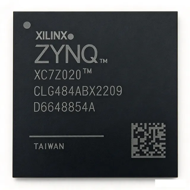
XC7Z020-1CLG484I - Zynq-7000 SoC 667MHz Dual ARM Cortex-A9 | AMD/Xilinx
XC7Z020-1CLG484I

XC7Z020-1CLG484I - Zynq-7000 SoC 667MHz Dual ARM Cortex-A9 | AMD/Xilinx

The AMD/Xilinx XC7Z020-1CLG484I is a Zynq-7000 All Programmable System-on-Chip (AP SoC) that integrates a dual-core ARM Cortex-A9 MPCore processing system with 667MHz core clock, together with Artix-7 programmable logic of 85K logic cells, all housed in a 484-ball CSBGA (CLG484) package measuring 19x19 mm. It is the -1 speed grade, industrial temperature range variant of the XC7Z020 family. A SoC FPGA such as the Zynq-7000 is a single silicon device that fuses a hard processor subsystem (HSS) and a soft FPGA fabric. The processor subsystem runs software (Linux, RTOS, bare-metal), while the programmable logic provides hardware acceleration, custom I/O, and parallel data-path extensions. Zynq-7000 devices sit within the broader taxonomy of heterogeneous compute devices, alongside MPSoC and Versal Adaptive SoC families from AMD/Xilinx. This hybrid architecture is ideal for embedded systems that require both deterministic real-time control and high-throughput data processing. Key features include dual ARM Cortex-A9 cores with NEON SIMD and single/double precision FPU, on-chip L1 caches (32 KB I-cache, 32 KB D-cache per core) and 512 KB L2 cache, integrated Memory Controller for DDR3/DDR3L/LPDDR2, dual USB 2.0 OTG, dual Gigabit Ethernet MACs, dual SD/SDIO controllers, and 2x UART, 2x SPI, 2x I2C peripheral interfaces. The integrated Artix-7 FPGA fabric includes 85K logic cells, 4.9 Mb block RAM, and 220 DSP slices. The Zynq-7000 architecture uses a tightly coupled AXI interconnect between the PS and PL, allowing hardware-accelerated peripherals to communicate with the processor at high bandwidth with predictable latency. The CLG484 package exposes multiple high-performance (HP) and high-range (HR) I/O banks for DDR interfacing and general-purpose I/O. Typical applications include industrial motor drives, machine vision, software-defined radio, ADAS driver assistance systems, medical imaging, and embedded vision. The wide temperature range and -1 speed grade make the XC7Z020-1CLG484I well suited for industrial control and factory automation. When designing with this device, careful attention must be paid to PCB layout, power-rail sequencing, and DDR signal integrity. Use Vivado Design Suite and Vitis for hardware/software co-design, and refer to the official Zynq-7000 datasheet (DS187) and PCB design guide (UG933). This page synthesizes distributor pricing, drop-in alternatives, and practical design notes not found in the manufacturer datasheet.

USD $45,94 Stokta
XC7Z020-2CLG484I - Zynq-7000 SoC 85K Logic Cells | AMD
XC7Z020-2CLG484I

XC7Z020-2CLG484I - Zynq-7000 SoC 85K Logic Cells | AMD

The AMD XC7Z020-2CLG484I is a Zynq-7000 All Programmable SoC (AP SoC) integrating a dual-core ARM Cortex-A9 MPCore processor with an Artix-7 class FPGA fabric in a single 484-ball CSPBGA (19x19 mm) package. The processor subsystem runs at up to 766 MHz with CoreSight debug, while the programmable logic provides 85,000 logic cells, 53,200 LUTs, 106,400 flip-flops, 220 DSP slices, and 4.9 Mb of block RAM. A System on Chip (SoC) is an integrated circuit that consolidates processor, memory controllers, peripherals, and programmable hardware on a single substrate. The Zynq-7000 family pairs an ARM-based processing system (PS) with programmable logic (PL) over high-bandwidth AXI interfaces, reducing board space, power, and system complexity versus discrete processor-plus-FPGA solutions. Key features include a DDR3/DDR3L memory controller with ECC, USB 2.0, Gigabit Ethernet, and support for I/O voltages of 1.2V, 1.5V, 1.8V, 2.5V, and 3.3V. The -2 speed grade supports up to 766 MHz PS operation and 200 MHz+ fabric clocking. The industrial temperature grade (-40C to +100C) targets harsh environments. Architecturally, the PS and PL are independent power domains with defined sequencing requirements (VCCINT, VCCAUX, VCCBRAM, VCCO). The device supports partial reconfiguration, allowing dynamic PL updates while the PS continues running. The memory controller delivers robust DDR3/DDR3L with ECC for industrial and automotive-class designs. Typical applications include motor control, industrial automation, software-defined radio, video processing, and embedded vision. The device suits real-time processing with hardware acceleration, such as machine vision and high-speed data acquisition. Design consideration: ensure correct power-rail sequencing and provide a configuration source (QSPI flash) and PS clock; refer to the Zynq-7000 TRM (UG585) for detailed guidance. Pricing from $60.07 (LCSC, as of 2026-08-29).

USD $49,00 İletişim
XC7Z030-1FB484I - 667MHz Zynq SoC | AMD | Industrial FPGA
XC7Z030-1FB484I

XC7Z030-1FB484I - 667MHz Zynq SoC | AMD | Industrial FPGA

The AMD XC7Z030-1FB484I is a Zynq-7000 Kintex-7 system-on-chip FPGA with 125K logic cells, dual ARM Cortex-A9 MPCore processors operating at 667 MHz, and CoreSight debug support, housed in a 484-FCBGA package measuring 23 x 23 mm. It combines programmable FPGA logic and a hard processor subsystem in one device, making it suitable for embedded control, industrial automation, networking, signal processing, and connected systems. A Zynq-7000 SoC FPGA integrates a programmable logic section with one or more ARM Cortex-A9 processors. The processor subsystem executes software, while the FPGA fabric implements parallel datapaths, custom interfaces, protocol engines, and control logic. This combination allows designers to place software-controlled functions and hardware-accelerated operations in one package instead of using a separate processor and FPGA. The XC7Z030-1FB484I provides 125K logic cells and a 667 MHz processor frequency according to the verified distributor listing. The part is identified as a speed-grade-1, industrial-temperature device by the verified FPGA Market listing. Its 484-FCBGA package provides 484 terminals in a 23 x 23 mm surface-mount format. Exact pin names, electrical limits, I/O standards, memory configuration, and power requirements were not included in the supplied source data and must be confirmed in the manufacturer datasheet. Typical designs use the programmable fabric for high-throughput parallel processing and the Cortex-A9 subsystem for operating-system support, networking, control loops, or application workloads. The integrated architecture can simplify a board-level partition when software and programmable logic must exchange data frequently. Engineers should still budget for external memory, clocking, power regulation, signal conditioning, and thermal management where the selected design requires them. The most important layout consideration is package escape routing. A 484-ball BGA device requires a substrate or PCB with compatible ball geometry, via-in-pad or fanout strategy, controlled impedance, and an assembly process capable of handling the package pitch. Verify the exact pinout and I/O assignments against AMD package documentation before schematic capture or PCB release. This page consolidates verified distributor and cross-reference results, separates confirmed specifications from missing parameters, and provides engineering guidance for evaluating this industrial Zynq SoC FPGA. It does not infer a drop-in replacement unless a manufacturer or distributor explicitly verifies the same package and pin compatibility.

RFQ İletişim
XC7Z030-1FBG484I - Zynq-7000 SoC, 125K Logic Cells | AMD
XC7Z030-1FBG484I

XC7Z030-1FBG484I - Zynq-7000 SoC, 125K Logic Cells | AMD

The AMD XC7Z030-1FBG484I is a Zynq-7000 SoC integrating a dual-core ARM Cortex-A9 MPCore processor with a Kintex-7 FPGA fabric. It features 125K logic cells, 667MHz maximum processor frequency, and comes in a 484-pin FCBGA package (23x23mm). This SoC combines the programmability of an FPGA with the performance of an embedded processor, enabling flexible system design for a wide range of applications. A System-on-Chip (SoC) integrates a processor, memory, and peripherals onto a single die, reducing board space and power consumption while improving reliability. The Zynq-7000 family specifically combines a hard ARM processor subsystem with programmable logic, allowing hardware acceleration and custom I/O. This hybrid architecture is ideal for applications requiring both high-level operating system support and real-time, low-latency processing. Key features include 125K logic cells, 667MHz dual-core ARM Cortex-A9, 256KB on-chip memory, and support for DDR3/DDR3L memory interfaces. The device also offers high-speed transceivers, PCIe Gen2, and multiple I/O standards. The -1 speed grade indicates a base performance level, while the I suffix denotes industrial temperature range (-40°C to +100°C). The Zynq-7000 architecture separates the processing system (PS) from the programmable logic (PL), connected via high-bandwidth AXI interfaces. This allows designers to optimize software and hardware independently. The PS includes a memory management unit, DMA controllers, and a rich set of peripherals, while the PL provides flexible logic resources for custom accelerators and interfaces. Typical applications include software-defined radio, industrial motor control, automotive driver assistance, and high-performance embedded computing. The combination of ARM processing and FPGA fabric makes it suitable for edge computing, where low latency and high throughput are critical. The industrial temperature grade ensures reliable operation in harsh environments. When designing with this SoC, careful attention must be paid to power supply sequencing and decoupling. The device requires multiple voltage rails (VCCINT, VCCAUX, VCCO) and proper power-on sequencing to avoid latch-up. Refer to the Zynq-7000 TRM (UG585) for detailed power-up requirements.

RFQ İletişim
XC7Z030-1SB485I - 667MHz Zynq SoC | AMD | Industrial Control
XC7Z030-1SB485I

XC7Z030-1SB485I - 667MHz Zynq SoC | AMD | Industrial Control

The AMD XC7Z030-1SB485I is a Zynq-7000 Kintex-7 system-on-chip with dual ARM Cortex-A9 MPCore processors operating at 667 MHz, 125,000 FPGA logic cells, and a 484-FCBGA package measuring 19 x 19 mm. The device combines programmable FPGA logic, ARM processing, memory interfaces, and connectivity in one high-integration package. A Zynq SoC is a heterogeneous embedded-processing device: the hard processor system executes operating-system and application software, while the Kintex-7 FPGA fabric implements parallel hardware, custom interfaces, accelerators, and real-time logic. This combination allows control software and hardware data paths to operate within one device, reducing board-level component count compared with separate FPGA and processor solutions. Key verified features include two ARM Cortex-A9 MPCore processors, CoreSight debug support, a 667 MHz processor clock, and approximately 125K Kintex-7 logic cells. The supplied distributor records identify the package as 484-FCBGA in a 19 x 19 mm body. Additional device details such as I/O count, memory-interface ratings, power rails, and automotive qualification are not supplied in the verified data and must be confirmed in the manufacturer documentation before schematic release. The FPGA fabric is suitable for parallel image-processing stages, protocol conversion, data acquisition, control logic, and hardware acceleration. The ARM subsystem supports embedded Linux, real-time operating systems, control loops, networking stacks, and supervisory software. Designers can partition functions between software and programmable logic according to latency, parallelism, and update requirements rather than forcing every operation into either domain. Typical implementations include industrial controllers, machine vision, test and measurement systems, embedded networking equipment, communications infrastructure, and high-performance embedded appliances. Programmable FPGA logic can accelerate filtering, protocol framing, or interface conversion, while the ARM subsystem manages configuration, telemetry, control, and application services. A new design should begin with the exact AMD device documentation and pin-level package information. The BGA footprint requires dense escape routing, many decoupling connections, careful power planning, and manufacturing controls capable of handling the 484-contact package. Because those electrical and layout requirements are not present in the supplied snippets, engineers must obtain the official datasheet, package files, schematic guidance, and board-design requirements before layout. This page combines verified distributor specifications and sourcing information with structured engineering guidance. It distinguishes confirmed facts from unavailable parameters, avoiding invented memory, power, I/O, and compliance claims while identifying the exact resources needed to qualify a production design.

RFQ İletişim
XC7Z030-2FB484I - Zynq-7000 SoC 800MHz Kintex-7 FPGA 484-FCBGA | AMD
XC7Z030-2FB484I

XC7Z030-2FB484I - Zynq-7000 SoC 800MHz Kintex-7 FPGA 484-FCBGA | AMD

The AMD Xilinx XC7Z030-2FB484I is a Zynq-7000 family System-on-Chip (SoC) that integrates a dual-core ARM Cortex-A9 MPCore hard processor system with Kintex-7 based programmable logic on a single 28nm device, packaged in a 484-ball FCBGA (23x23 mm) and rated for the industrial -40C to +100C temperature range. The SoC combines a hardened processing subsystem (PS) running up to 800 MHz with a Kintex-7 fabric delivering 125K logic cells, making it a heterogeneous compute device for embedded vision, industrial control, and software-defined radio applications. The 'I' suffix indicates industrial temperature grade and the '2' speed grade denotes a mid-tier performance bin, balancing static timing margin against power consumption. What is a Zynq SoC? A Zynq-7000 System-on-Chip is a heterogeneous device that pairs ARM Cortex-A9 application processor cores with Xilinx Kintex-7 (or Artix-7) FPGA fabric through high-bandwidth AXI interconnects. Unlike a pure FPGA, the Zynq boots and runs C/C++ code natively while exposing programmable logic for hardware acceleration, custom peripherals, and parallel DSP pipelines. It sits in the hierarchy: Zynq-7000 -> SoC -> embedded processor + FPGA hybrid -> semiconductor device, and is widely used in embedded computing platforms including ZC702 evaluation boards and custom carrier cards. Key architectural features include dual Cortex-A9 cores with NEON SIMD and single/double precision floating point, ARM CoreSight debug, hardware block RAM (BRAM), DSP48E1 slices, multiplexed I/O (MIO) and extended MIO (EMIO), and integrated memory controllers supporting DDR3/DDR3L/LPDDR2. The Kintex-7 fabric provides 125K logic cells, approximately 9.4 Mb of block RAM, and DSP48E1 slices suitable for FIR filters, FFT engines, and high-throughput signal processing. The part integrates GTX (Gigabit Transceiver) hard IP for multi-gigabit serial links in the higher-density Zynq-7000 family variants. Typical applications include machine vision and video pipelines, software-defined radio (SDR) baseband, industrial motor control with EtherCAT, ADAS prototyping, medical imaging front-ends, and custom embedded compute platforms where Linux or RTOS runs on the Cortex-A9 while the FPGA fabric accelerates PCIe, custom I/O, or DSP functions. The 800 MHz Cortex-A9 frequency enables real-time control loops and multimedia workloads. Power-supply decoupling follows Xilinx ug583, and PCB signal-integrity routing follows ug583/ug587 guidance for the MIO/EMIO DDR interfaces. When designing with this part, ensure your Vivado Design Suite and Vitis IDE versions match the silicon revision listed in the device DNA register. Pin-compatible same-package Zynq-7000 variants allow migration up or down the family (Z-7010/Z-7015/Z-7020/Z-7030/Z-7035/Z-7045/Z-7100) on the same 484-ball FCBGA footprint, enabling platform reuse across SKUs. This page synthesizes drop-in package-compatible alternatives, parametric comparison data, and practical PCB design notes specific to the XC7Z030-2FB484I - context not assembled on any single distributor product page.

RFQ İletişim
XC7Z030-2FBG484I - Zynq-7000 SoC, 125K Logic Cells | AMD
XC7Z030-2FBG484I

XC7Z030-2FBG484I - Zynq-7000 SoC, 125K Logic Cells | AMD

The AMD XC7Z030-2FBG484I is a Zynq-7000 family System-on-Chip (SoC) that integrates a dual-core ARM Cortex-A9 MPCore processing system with a Kintex-7 class programmable logic fabric. This device combines the flexibility of an FPGA with the performance of an embedded processor, making it ideal for a wide range of applications including software-defined radio, industrial automation, and automotive driver assistance systems. The device is housed in a 484-pin FCBGA package (23x23 mm) and operates over the industrial temperature range of -40°C to +100°C. A System-on-Chip (SoC) is an integrated circuit that consolidates all components of a computer or other electronic system into a single chip. The Zynq-7000 family specifically combines a hard processing system (PS) with programmable logic (PL), allowing designers to implement custom hardware accelerators alongside software applications. This architecture bridges the gap between traditional microprocessors and FPGAs, enabling high-performance, low-latency processing for demanding embedded applications. Key features of the XC7Z030-2FBG484I include 125,000 logic cells, a dual-core ARM Cortex-A9 processor running at up to 800 MHz, and support for 1.2V to 3.3V I/O standards. The device also includes 256 KB of on-chip memory, integrated PCIe, and multiple high-speed transceivers. These features provide a powerful and flexible platform for implementing complex digital systems. From a technical perspective, the XC7Z030-2FBG484I is fabricated using a 28nm process technology, which balances performance and power efficiency. The processing system includes a memory management unit, L1 and L2 caches, and a wide range of peripherals, while the programmable logic is based on the Kintex-7 architecture, offering high logic density and DSP capabilities. This combination allows for the implementation of sophisticated algorithms and interfaces. Typical applications for the XC7Z030-2FBG484I include software-defined radio, where the programmable logic handles baseband processing and the ARM cores run protocol stacks; industrial motor control, where the FPGA implements high-speed PWM and the processor handles communication; and medical imaging, where the device accelerates image processing algorithms. The device's high-speed transceivers also make it suitable for video and network processing. When designing with this device, careful attention must be paid to power supply decoupling and thermal management. The 484-pin FCBGA package requires a multi-layer PCB with dedicated power and ground planes. The device's power consumption can be significant, so a proper heatsink or active cooling solution may be necessary for high-performance applications.

RFQ İletişim
XC7Z030-2SBG485I - Zynq-7000 SoC, 125K Logic Cells | AMD
XC7Z030-2SBG485I

XC7Z030-2SBG485I - Zynq-7000 SoC, 125K Logic Cells | AMD

The AMD XC7Z030-2SBG485I is a Zynq-7000 family System-on-Chip (SoC) that integrates a dual-core ARM Cortex-A9 MPCore processing system with a Kintex-7 class programmable logic fabric. This device combines the flexibility of an FPGA with the performance of an embedded processor, making it ideal for a wide range of applications including automotive, medical, and industrial systems. The device is housed in a 484-ball FCBGA package (19x19 mm) and operates at a maximum frequency of 800 MHz. A System-on-Chip (SoC) is an integrated circuit that consolidates all components of a computer or other electronic system into a single chip. The Zynq-7000 family specifically merges a hard ARM-based processing system (PS) with programmable logic (PL), allowing designers to implement custom hardware accelerators alongside software applications. This architecture enables high-performance, low-latency processing that is not achievable with traditional microprocessors or FPGAs alone. Key features of the XC7Z030-2SBG485I include 125,000 logic cells, dual ARM Cortex-A9 cores running at 800 MHz, and a 28nm process technology. The device supports a wide range of I/O standards and includes high-speed transceivers for serial communication. The 'I' suffix indicates an industrial temperature grade, with an operating range of -40°C to +100°C, making it suitable for harsh environments. From a technical perspective, the Zynq-7000 architecture provides a high-bandwidth interconnect between the PS and PL, enabling efficient data transfer. The device includes a memory management unit (MMU) for the ARM cores, as well as a rich set of peripherals including USB, Ethernet, and SPI. The programmable logic can be configured to implement custom peripherals, DSP blocks, or even soft-core processors, offering unparalleled design flexibility. Typical applications for the XC7Z030-2SBG485I include software-defined radio, motor control, image processing, and automotive driver assistance systems. The combination of a powerful processor and reconfigurable logic makes it an excellent choice for systems that require both high-level control and real-time signal processing. When designing with this device, careful attention must be paid to power supply decoupling and thermal management. The FCBGA package requires a well-designed PCB with adequate ground planes and thermal vias to ensure reliable operation at high temperatures.

RFQ İletişim
XC7Z035-2FFG676I - Zynq-7000 SoC, 275K LC, 800MHz | AMD
XC7Z035-2FFG676I

XC7Z035-2FFG676I - Zynq-7000 SoC, 275K LC, 800MHz | AMD

The AMD (Xilinx) XC7Z035-2FFG676I is a Zynq-7000 All Programmable System-on-Chip (SoC) combining a dual-core ARM Cortex-A9 MPCore processing system running at 800 MHz with a Kintex-7 class FPGA fabric of 275K logic cells, housed in a 676-ball FCBGA (27x27 mm) industrial-grade package. A Zynq-7000 SoC is a class of programmable system-on-chip devices that integrate a hardwired processor system (PS) with programmable logic (PL) on a single die. Unlike a standalone FPGA or a standalone microprocessor, a SoC FPGA allows software running on the ARM cores and hardware accelerators in the fabric to communicate over high-bandwidth on-chip AXI interconnect, making the device family a cornerstone of modern embedded processing and adaptive computing hierarchies. Key features of the XC7Z035 include the mid-range 275K logic cell fabric, a -2 speed grade, and industrial temperature screening (the I suffix, typically -40C to +100C junction), making it suitable for harsh-environment deployments. The hard processor system offloads control-plane software while the fabric absorbs data-plane acceleration, math, and custom I/O. Architecturally, the device pairs the ARM Cortex-A9 NEON/FPU-enabled cores with CoreSight debug, caches, on-chip memory, and a rich set of PS peripherals, bonded to Kintex-7-based programmable logic with DSP slices, block RAM, and high-speed serial transceivers. AXI ports bridge the two domains with low latency. Typical applications include industrial automation and motor control, aerospace and defense processing, software-defined radio, video and image processing pipelines, and network packet processing where a soft processor would be too slow and a discrete CPU+FPGA pair too costly. When designing with this device, plan power sequencing between VCCINT, VCCAUX, and PS rails, and select a Vivado device name matching the industrial speed-grade variant to avoid implementation errors. This page synthesizes distributor pricing, verified same-package drop-in alternatives, and practical design notes not found in the manufacturer datasheet alone.

RFQ İletişim
XC7Z045-1FBG676I - Zynq-7000 SoC, 350K Logic Cells | AMD
XC7Z045-1FBG676I

XC7Z045-1FBG676I - Zynq-7000 SoC, 350K Logic Cells | AMD

The AMD XC7Z045-1FBG676I is a Zynq-7000 family System-on-Chip (SoC) that integrates a dual-core ARM Cortex-A9 MPCore processor with a Kintex-7 FPGA fabric. It is housed in a 676-pin FCBGA package (27x27 mm) and operates at a maximum clock frequency of 667 MHz. The device provides 350K logic cells, making it suitable for high-performance embedded applications requiring both software programmability and hardware flexibility. A System-on-Chip (SoC) is an integrated circuit that combines multiple system components, such as processors, memory interfaces, and I/O, onto a single substrate. The Zynq-7000 family specifically merges a processing system (PS) based on ARM cores with programmable logic (PL) based on FPGA fabric. This architecture allows designers to implement complex algorithms in hardware while maintaining the flexibility of software-defined control, bridging the gap between traditional microprocessors and FPGAs. Key features of the XC7Z045-1FBG676I include 350K logic cells, 256 KB of on-chip RAM, and support for high-speed transceivers. The device also includes a rich set of I/O options, including multiple high-speed serial transceivers and general-purpose I/O banks. The dual-core ARM Cortex-A9 processor runs at up to 667 MHz, providing substantial processing power for real-time applications. From a technical perspective, the XC7Z045-1FBG676I leverages AMD's advanced 28nm process technology, balancing performance and power efficiency. The integration of the ARM processor with the Kintex-7 FPGA fabric enables low-latency, high-bandwidth communication between software and hardware, which is critical for applications like software-defined radio, image processing, and industrial control. The device supports a wide range of industry-standard interfaces, including DDR3/DDR4 memory controllers and PCIe. Typical applications include high-end embedded computing, aerospace and defense systems, medical imaging, and wired/wireless communications. The combination of a powerful processor and reconfigurable logic makes it ideal for prototyping and production in demanding environments. When designing with this device, careful attention must be paid to power supply sequencing and decoupling. The multiple power rails require proper sequencing to avoid latch-up or damage. Additionally, the high-speed transceivers demand clean power and careful PCB layout to maintain signal integrity.

RFQ İletişim
XC7Z045-1FFG900I - Zynq-7000 SoC, 350K Logic Cells | AMD
XC7Z045-1FFG900I

XC7Z045-1FFG900I - Zynq-7000 SoC, 350K Logic Cells | AMD

The AMD XC7Z045-1FFG900I is a Zynq-7000 SoC that integrates a dual-core ARM Cortex-A9 MPCore processing system (PS) with a 28nm Kintex-7-class programmable logic (PL) fabric in a single device. It is housed in a 900-ball FCBGA package (31x31 mm) and operates at a maximum PS clock frequency of 667 MHz. This SoC provides 350K logic cells, making it a high-capacity platform for embedded systems that require both software flexibility and hardware acceleration. A System-on-Chip (SoC) FPGA combines a hard processor subsystem with programmable logic on one die. The Zynq-7000 family, introduced by Xilinx (now AMD) in 2012, is a leading example of this architecture. It allows designers to implement complex systems where the ARM cores handle control and communication tasks, while the FPGA fabric accelerates data-intensive algorithms. This integration reduces board space, power, and latency compared to discrete processor-plus-FPGA designs. Key features of the XC7Z045-1FFG900I include 350K logic cells, 667 MHz dual-core ARM Cortex-A9 processing, and a 900-ball FCBGA package. The device supports a wide range of I/O standards and includes high-speed serial transceivers. The 'I' suffix indicates an industrial temperature grade, suitable for harsh environments. The '1' speed grade offers a balance between performance and power consumption. The Zynq-7000 architecture provides a high-bandwidth connection between the PS and PL through AXI interfaces, enabling efficient data movement. The PL is based on the 7-series FPGA fabric, which includes configurable logic blocks, block RAM, and DSP slices. This allows for the implementation of custom accelerators, soft processors, and high-speed I/O interfaces. The PS includes memory controllers for DDR3/DDR3L, as well as a rich set of peripherals such as Gigabit Ethernet, USB, and SPI. Typical applications for the XC7Z045-1FFG900I include software-defined radio, industrial motor control, medical imaging, and aerospace and defense systems. Its combination of processing power and programmable logic makes it ideal for applications requiring real-time signal processing, high-speed data acquisition, and flexible I/O. The industrial temperature grade ensures reliable operation in demanding environments. When designing with this SoC, careful attention must be paid to power supply sequencing and decoupling. The device requires multiple voltage rails, and proper sequencing is critical to prevent damage. Additionally, the high-density BGA package requires a multi-layer PCB with controlled impedance traces for high-speed signals. AMD provides comprehensive reference designs and documentation to assist with these challenges.

RFQ İletişim
XC7Z045-2FBG676I - Zynq-7000 SoC, 350K Logic Cells | AMD
XC7Z045-2FBG676I

XC7Z045-2FBG676I - Zynq-7000 SoC, 350K Logic Cells | AMD

The AMD XC7Z045-2FBG676I is a Zynq-7000 family System-on-Chip (SoC) that integrates a dual-core ARM Cortex-A9 MPCore processing system with a Kintex-7 class programmable logic fabric. This device combines the flexibility of an FPGA with the performance of an embedded processor, making it ideal for a wide range of applications including software-defined radio, industrial motor control, and high-performance video processing. The XC7Z045-2FBG676I features 350K logic cells, 800MHz maximum processor clock speed, and is housed in a 676-ball FCBGA (27x27mm) package. A System-on-Chip (SoC) is an integrated circuit that consolidates all components of a computer or other electronic system into a single chip. It typically includes a processor core, memory, input/output ports, and secondary storage interfaces. In the context of the Zynq-7000 family, the SoC combines a hard processing system (PS) based on ARM Cortex-A9 cores with programmable logic (PL) based on FPGA fabric. This architecture allows designers to implement custom hardware accelerators in the PL while running operating systems like Linux on the PS, offering a balance of performance, flexibility, and power efficiency. Key features of the XC7Z045-2FBG676I include 350K logic cells, 800MHz dual-core ARM Cortex-A9 processor, 16.25 Mb of block RAM, and 900 DSP slices. The device supports a wide range of I/O standards and includes high-speed transceivers for serial communication. The -2 speed grade indicates a high-performance variant, suitable for demanding applications. The industrial temperature grade (I suffix) allows operation from -40°C to +100°C, making it suitable for harsh environments. The Zynq-7000 architecture provides a unique advantage by enabling tight coupling between the processing system and programmable logic through an AMBA AXI interconnect. This allows for high-bandwidth, low-latency communication between software running on the ARM cores and custom hardware logic. The device also includes a memory management unit, DDR3/DDR3L memory controller, and various peripheral interfaces such as USB, Gigabit Ethernet, and SDIO, enabling a complete embedded system on a single chip. Typical applications for the XC7Z045-2FBG676I include software-defined radio, where the programmable logic handles baseband processing while the ARM cores run protocol stacks; industrial motor control, where custom PWM and encoder interfaces are implemented in logic; and high-performance video processing, where the PL accelerates image processing algorithms. The device is also used in aerospace and defense applications requiring high reliability and long-term availability. When designing with this device, careful attention must be paid to power supply decoupling and thermal management. The FCBGA package requires a well-designed PCB with adequate thermal vias and a heatsink for high-power applications. The device supports multiple power rails (VCCINT, VCCAUX, VCCO) that must be sequenced correctly during power-up to prevent damage.

RFQ İletişim
XC7Z045-2FF900I - 350K Zynq SoC | AMD | Industrial FPGA
XC7Z045-2FF900I

XC7Z045-2FF900I - 350K Zynq SoC | AMD | Industrial FPGA

AMD XC7Z045-2FF900I is a Zynq-7000 Kintex-7 FPGA system on chip with 350,000 logic cells, 800 MHz processing capability, 19,558 Kb of block RAM, 900 DSP slices, and a 900-FCBGA (31 x 31 mm) package. The -2 ordering code identifies speed grade 2, while the I suffix identifies the industrial temperature option. Its industrial junction-temperature range is -40 °C to 100 °C. A Zynq-7000 SoC is a heterogeneous programmable-logic device that combines ARM Cortex-A9 processing hardware with Kintex-7 FPGA fabric in one package. This integration places a hard processor subsystem, programmable logic, programmable I/O, memory resources, and DSP resources within a single mixed-signal device. It belongs to the FPGA and SoC hierarchy and can consolidate control processing, parallel data acquisition, and programmable signal processing into one board-level platform. The XC7Z045 provides approximately 350,000 logic cells, 19,558 Kb of block RAM, and 900 DSP slices. Its dual-core ARM Cortex-A9 subsystem is suitable for standalone control software, while the Kintex-7 fabric can implement parallel datapaths, interface logic, protocol handling, and custom accelerators. The 800 MHz figure and CoreSight support identify a high-performance embedded processing configuration designed for demanding control and signal-processing systems. The FF900 package provides 900 solderable FCBGA positions in a 31 x 31 mm land pattern. This high pin count supports the device's extensive power, ground, signal, configuration, and high-speed I/O requirements. The package also creates demanding PCB-layout, assembly, thermal, and decoupling obligations, particularly around power delivery to the processor, FPGA fabric, memory interfaces, and transceiver-related I/O. Typical applications include industrial machine vision, industrial automation, communications infrastructure, test and measurement, embedded signal processing, and high-performance control systems. In these systems, the ARM subsystem can execute operating-system or bare-metal software while the programmable logic handles deterministic acquisition, filtering, protocol parsing, and data movement without relying solely on software execution. Designers should preserve the XC7Z045 power rails, decoupling network, configuration interface, clocking scheme, and DDR memory topology defined by the AMD hardware design guidance. The 900-FCBGA package also requires adequate thermal design and assembly process control. Package, operating-temperature, and several detailed electrical specifications remain unavailable in the supplied verified dataset and are therefore identified rather than estimated. This product record combines verified AMD and distributor data with package-aware alternatives, comparison parameters, and practical design guidance. It distinguishes exact same-package order variants from candidates requiring further qualification, helping engineers make sourcing and design decisions without treating electrical similarity as proof of drop-in compatibility.

RFQ İletişim
XC7Z100-1FF900I - Dual Cortex-A9 Zynq SoC | AMD
XC7Z100-1FF900I

XC7Z100-1FF900I - Dual Cortex-A9 Zynq SoC | AMD

AMD XC7Z100-1FF900I is a Zynq-7000 system on chip with dual Arm Cortex-A9 MPCore processors, CoreSight debug capability, 444K Kintex-7 FPGA logic cells, a 667 MHz processor rating, and a 900-FCBGA package measuring 31 x 31 mm. It combines programmable logic, hard processor, memory interfaces, and high-speed connectivity in one device. A Zynq-7000 system on chip is an FPGA and ARM processor integration. In the product hierarchy, it is a system on chip, programmable logic device, FPGA, and embedded processor platform. The processor subsystem executes operating-system-level and application software, while the Kintex-7 programmable logic fabric implements parallel data paths, interfaces, signal processing, and other hardware-specific functions. This combination enables hardware/software partitioning without requiring two separate chips and associated interconnects. The verified device description identifies two Arm Cortex-A9 MPCore processors and CoreSight technology. It provides 444K logic cells for programmable FPGA resources and lists a 667 MHz operating frequency for the processor configuration. The 900-FCBGA package offers 900 solder balls in a 31 x 31 mm footprint. The listed LCSC price is $9,547.7967 as of October 28, 2026, reflecting the scale and specialized nature of this programmable SoC. Technically, the XC7Z100 belongs to the Zynq-7000 family and combines an ARM hard-processing subsystem with Xilinx Kintex-7 FPGA logic. CoreSight provides integrated processor debug and trace visibility. The same silicon package can support designs that divide work between sequential software and parallel programmable hardware, reducing external component count when application requirements align with the integrated architecture. Typical uses include industrial control, machine vision, network infrastructure, test and measurement, embedded signal processing, and communications equipment. Developers can implement hardware acceleration, custom interfaces, protocol handling, and data acquisition alongside application code. The 444K logic-cell fabric is especially useful where deterministic parallel operations, custom I/O, or high-throughput data paths are required. Design planning must include a 900-ball PCB land pattern, power and multi-rail sequencing, decoupling, thermal management, and programming-device support. Differential I/O and high-speed memory interfaces also require controlled routing and verification. A new layout should be compared directly with AMD package-pinout files rather than inferred from generic BGA conventions. This page combines the verified distributor data, official AMD datasheet link, package-pinout resource, and engineering-focused selection guidance. It also distinguishes the verified 667 MHz target from faster same-family alternatives and clearly identifies where distributor-specific electrical, lifecycle, or package details require confirmation before procurement.

RFQ İletişim
XC7Z100-2FF900I - Zynq-7000 444K SoC | AMD Xilinx
XC7Z100-2FF900I

XC7Z100-2FF900I - Zynq-7000 444K SoC | AMD Xilinx

The AMD Xilinx XC7Z100-2FF900I is a Zynq-7000 programmable SoC integrating a dual ARM Cortex-A9 MPCore processor with a Kintex-7 FPGA in a 900-FCBGA package. The device provides 444K logic cells, operates the ARM Cortex-A9 subsystem at 800 MHz, and is offered in the industrial -2 speed and temperature grade indicated by the I suffix. A Zynq-7000 SoC is a heterogeneous programmable system-on-chip that combines an ARM processing system, programmable logic, programmable I/O, memory controllers, and high-speed serial transceivers in one device. In the broader semiconductor hierarchy, it belongs to the field-programmable gate array family while adding a hard processor subsystem. This integration allows software-controlled systems to implement parallel hardware logic alongside a conventional Linux or bare-metal application processor. The XC7Z100-2FF900I headline resources are 444K Kintex-7 logic cells, an 800 MHz dual-core ARM Cortex-A9 configuration, and a 900-FCBGA package measuring 31 mm by 31 mm. It is positioned for designs requiring substantial parallel processing, high-speed connectivity, and an integrated real-time control architecture. The -2 device grade targets performance-oriented systems, while the I designation identifies the industrial temperature option. The integrated ARM Cortex-A9 MPCore subsystem supports a coherent dual-core application-processing environment, while the Kintex-7 fabric provides hardware acceleration for image processing, protocol handling, control loops, data acquisition, and custom peripheral logic. CoreSight debug resources accompany the processor and programmable logic, supporting design validation and post-silicon debugging. Exact fabric interface speeds, memory interface ratings, transceiver counts, and power envelopes were not included in the supplied source data and should be confirmed in the manufacturer data sheet. Typical deployments include industrial machine vision, high-speed inspection, laboratory instrumentation, industrial networking, embedded signal processing, and communications infrastructure. A video-processing design can assign pixel pipelines to programmable logic while the ARM subsystem runs control software and networking tasks. A deterministic acquisition system can use dedicated FPGA logic for sampling and buffering while the processor performs analysis, configuration, and external communications. Design planning must account for the package's 900 solder balls, multiple power rails, high-speed differential interfaces, and substantial thermal requirements. Follow the Zynq-7000 power-sequencing requirements, decouple each supply rail at the package pins, route high-speed pairs with controlled impedance, and provide a board-level thermal design appropriate for the selected performance class. This page consolidates distributor pricing, verified product descriptions, family-level alternatives, package information, and practical design guidance. It also identifies specifications that were not present in the supplied verification data so that engineers can distinguish confirmed values from items requiring confirmation against the AMD data sheet before layout or sourcing decisions.

RFQ İletişim
XC7Z100-2FFG900I - Zynq-7000 SoC, Kintex-7 FPGA, 444K Logic Cells | AMD
XC7Z100-2FFG900I

XC7Z100-2FFG900I - Zynq-7000 SoC, Kintex-7 FPGA, 444K Logic Cells | AMD

The AMD/Xilinx XC7Z100-2FFG900I is a Zynq-7000 All Programmable System-on-Chip (AP SoC) that integrates a dual-core ARM Cortex-A9 MPCore processor (up to 800 MHz) with a Kintex-7 FPGA fabric (444K logic cells, 26.5 Mb block RAM, 1540 DSP slices) in a single 900-ball FCBGA package (31x31 mm). It combines software programmability with hardware programmability, enabling hardware acceleration of compute-intensive workloads. A Zynq-7000 SoC is a heterogeneous multiprocessor device that fuses a Processing System (PS) - a dual ARM Cortex-A9 with NEON SIMD engines, caches, MMU, and standard peripherals - with Programmable Logic (PL) equivalent to a Kintex-7 FPGA. The PS boots first and configures the PL at start-up, allowing software designers to use familiar Cortex-A9 toolchains (GCC, Linux, FreeRTOS) while hardware designers accelerate critical paths in the PL. The XC7Z100 sits at the top of the Zynq-7000 family, sharing the Kintex-7 fabric with the Z-7045 but adding extra logic, DSP, and block RAM resources. Key features include 2x ARM Cortex-A9 cores at up to 800 MHz, 444K logic cells, 26.5 Mb block RAM, 1540 DSP48E1 slices, 16 GTX transceivers at up to 6.25 Gb/s, dual 12-bit 1 MSPS ADCs (XADC), 4x PCIe Gen2 hard blocks, and 2x USB 2.0 OTG ports. The integrated CoreSight debug enables multicore trace, and security features include AES, SHA, and RSA hardware accelerators alongside secure boot. Typical applications include high-performance embedded vision (machine-learning inference, ADAS front cameras), 8K video processing, software-defined radio baseband, industrial motor control with deterministic real-time loops, and avionics/medical imaging. The Kintex-7 PL is well suited to DSP-heavy algorithms like FFT, LDPC, and H.265 codec blocks. When designing, allocate decoupling and bulk capacitors close to each power rail (VCCPINT, VCCPAUX, VCCO, VCCAUX, MGTAVCC); use the AMD-recommended power-on/-off sequencing; and adopt the UG865 ASCII package files when laying out the 900-ball FCBGA. For evaluation, the ZC706 board (XC7Z045 in FFG900) is pin-compatible with the XC7Z100 FFG900 footprint, which AMD documents as an authorized Z-7100 reference platform.

RFQ İletişim
XC8664FRIBEKXUMA1 - 8-bit XC800 MCU, 16KB Flash, 38-TSSOP | Infineon
XC8664FRIBEKXUMA1

XC8664FRIBEKXUMA1 - 8-bit XC800 MCU, 16KB Flash, 38-TSSOP | Infineon

The Infineon XC8664FRIBEKXUMA1 is an 8-bit microcontroller built around the XC800 family 8051-compatible CISC core, integrating 16 KB of on-chip Flash memory, 16 KB (16K x 8) program Flash, and 38-pin TSSOP packaging. It operates from a wide supply range of 2.5 V / 3.3 V / 5 V and runs the 8051 core up to 86 MHz (with peripheral domain scaling at 26.67 MHz per the Hotenda listing). According to the manufacturer datasheet, this IC is the first product of a new and advanced 8-bit uC family (XC8oo family), combining a high-performance 8051 core with on-chip Flash memory and powerful on-chip peripherals. An 8-bit microcontroller (MCU) is a single-chip computer that integrates a CPU, RAM, non-volatile program memory, and peripherals such as timers, ADC, and communication interfaces. The 8051 CISC architecture, originally introduced by Intel in 1980, remains one of the most widely deployed embedded cores worldwide and underpins the hypernym hierarchy 8051 -> 8-bit MCU -> microcontroller -> embedded processor -> semiconductor. The XC8664FRIBEKXUMA1 belongs to Infineon's XC866 sub-family, which is targeted at cost-sensitive industrial and automotive body applications requiring deterministic 8-bit performance. Key differentiating features include a TSSOP-38 footprint with gull-wing leads, automotive temperature grade, integrated 16 KB Flash that supports in-application programming, an on-chip ADC and Capture/Compare Unit (CCU6), and a MultiCAN node for automotive networking. The 86 MHz core clock enables high-throughput bit-manipulation routines typical of motor-control and sensor-interface code, while the wide 2.5 V to 5 V supply range simplifies integration into 3.3 V and 5 V mixed-rail systems without external level shifters. The architecture pairs the standard 8051 instruction set with an XC800-specific peripheral set, including the MultiCAN module, the CCU6 motor-control timer, and a 10-bit ADC with up to eight channels. The wide operating voltage window (2.5 V to 5 V) is a defining trait of the XC8oo family and removes the need for separate voltage regulators in many 3.3 V or 5 V designs. Internal PLL, oscillator, and brown-out circuitry further reduce the external BOM. Typical applications include automotive body electronics, sensor interface modules, low-end motor control, and industrial control. The on-chip MultiCAN node makes the part particularly attractive for in-cabin nodes communicating over a CAN bus at 100 kbit/s to 1 Mbit/s. Designers should note that this part is in the older XC8xx family; current Infineon 8-bit roadmaps have shifted to the XC2000 and AURIX families, so lifecycle planning is recommended before committing to long-life designs.

RFQ İletişim