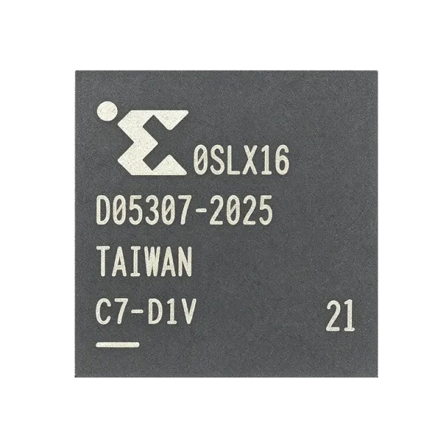
XC6SLX150T-2FG676I
XC6SLX150T-2FG676I - 147443-Cell Spartan-6 LXT FPGA | Xilinx
The Xilinx XC6SLX150T-2FG676I is a Spartan-6 LXT field-programmable gate array with 147,443 logic cells, 45 nm process technology, a 1.2 V supply, and a 676-pin FBGA package. It is positioned for industrial, communications, embedded, and signal-processing designs requiring a high-density programmable logic fabric and extensive fixed I/O resources. The -2 speed grade provides a defined performance class within the Spartan-6 LXT family, while the industrial I suffix identifies the specified operating-temperature and qualification grade.
An FPGA is a programmable semiconductor that replaces logic built from individual gates with a configurable array of programmable logic blocks, block RAM, DSP resources, programmable I/O, dedicated clocking, and high-speed serial transceivers. Within the product hierarchy, the XC6SLX150T belongs to the Spartan-6 LXT FPGA family, a 45 nm FPGA platform combining configurable logic with memory, digital signal processing, high-speed connectivity, and clock-management resources. The T designation identifies the LXT-family device rather than the LX family.
The principal headline features are 147,443 logic cells, a 676-pin surface-mount FBGA package, and operation from a 1.2 V core supply. The device uses the -2 speed grade, and the I suffix identifies the industrial-temperature variant. The Spartan-6 LXT family is available in -3, -3N, and -2 speed grades, with -3 providing the highest listed performance class and -2 serving as the grade represented by this part. Its 45 nm implementation supports a broad combination of programmable logic, embedded memory, DSP blocks, and serial connectivity.
The XC6SLX150T-2FG676I is designed for systems where interface count, deterministic programmable logic, parallel processing, and design flexibility matter more than minimum unit cost. Its high logic-cell count can support multiple independent processing channels, protocol bridges, datapath control, image or signal pipelines, and supervisory logic within one device. Dedicated block RAM and DSP resources can reduce the need for external memories or discrete processing components when the design maps efficiently into the FPGA architecture. A 676-pin package also provides a broad pin count for external memory, clocks, control signals, and high-speed I/O.
Typical uses include industrial control and factory automation, networking and communications infrastructure, instrumentation, test and measurement, embedded video processing, radar or signal-processing front ends, and high-reliability industrial equipment. The large pin count is particularly useful when a design requires substantial parallel connectivity, while the LXT feature set allows designers to combine conventional programmable logic with dedicated high-speed serial transceivers and DSP functions.
Design planning should account for BGA PCB construction, power-supply sequencing, decoupling, thermal management, and the high pin count. The manufacturer datasheet and package drawings should govern land patterns, ball assignments, and exposed-pad or thermal-via requirements. Timing closure also depends on the selected -2 speed grade, clocking architecture, I/O standards, and memory interface topology, so system-level constraints must be entered into the FPGA design tools before placement and routing are finalized.
This product page combines the exact orderable MPN, package information, family identity, lifecycle context, structured specifications, direct replacement candidates, and engineering guidance for PCB and design planning. It also distinguishes true same-package drop-in options from parts that require a different package or a redesigned circuit, helping engineers shortlist replacements without treating merely similar FPGAs as electrically and mechanically interchangeable.
RFQ
İletişim