Ürünler (46.000+)

LM2416CT - Triple 35MHz Video Amplifier | Texas Instruments
LM2416CT

LM2416CT - Triple 35MHz Video Amplifier | Texas Instruments

Texas Instruments LM2416CT is a triple-channel video amplifier and CRT driver with a bandwidth of 35 MHz, output-current capability of 22 mA per channel, and an 11-terminal TO-220 through-hole package. The device is intended for driving analog video signals in CRT-based display equipment and related low-impedance video interfaces. A video amplifier is a specialized amplifier category designed to preserve amplitude and timing relationships across a wide frequency range. Within the signal-chain hierarchy, the LM2416CT combines three video amplifier channels in one package, reducing component count in multi-channel display systems. Its TO-220-11 construction also provides a substantial thermal path compared with small-outline surface-mount packages. The principal feature of the LM2416CT is its three-channel architecture. Each channel can deliver up to 22 mA, allowing it to support video-cathode drive requirements rather than serving only as a low-current signal-conditioning amplifier. Its 35 MHz bandwidth provides adequate margin for conventional analog CRT video signals while keeping the circuit manageable in legacy display designs. The LM2416C family is described as a triple 50 MHz CRT driver in the National Semiconductor documentation, while current distributor records identify the LM2416CT as a 35 MHz triple video-amplifier device. These descriptions should be checked against the applicable revision of the manufacturer datasheet when designing new equipment, particularly when bandwidth, gain, settling behavior, or output-stage limits are critical. Typical applications include CRT monitor video-output boards, multi-channel analog video distribution, laboratory display equipment, and legacy industrial or medical visualization systems. The 11-lead formed TO-220 package makes the LM2416CT most practical in through-hole and repair-oriented assemblies where a robust heat-dissipation path is more important than compactness. Designers should preserve adequate copper area around the device, provide a clean bypass supply, and follow the manufacturer pin configuration when routing the three channels. Because it is a legacy video-output component, verify connector standards, video bandwidth requirements, thermal conditions, and replacement availability before beginning a new production design. This page organizes the LM2416CT’s known channel count, bandwidth, current capability, package, sourcing information, comparison candidates, and application guidance into one engineering-focused reference for evaluating legacy analog video drive designs.

RFQ İletişim
LM2416T - Triple 50 MHz CRT Video Driver | National Semiconductor
LM2416T

LM2416T - Triple 50 MHz CRT Video Driver | National Semiconductor

National Semiconductor LM2416T is a triple 50 MHz CRT video driver integrated circuit packaged in an 11-lead TO-220 configuration. The device provides three video output channels for driving analog CRT displays, combining video amplification and output drive functions in one package. Its 50 MHz bandwidth class is suited to legacy graphics systems operating with conventional CRT monitors, including VGA-class video outputs and other analog display interfaces. A CRT video driver is an amplifier IC that converts a low-level video signal into the higher-level drive voltage required by a cathode-ray tube. In the product hierarchy, the LM2416T is a video amplifier within the broader amplifier IC and integrated-circuit categories. It belongs to a class of devices designed specifically for analog display outputs rather than modern flat-panel interfaces such as HDMI, DisplayPort, or LVDS. The principal documented features include three video output channels and a maximum video bandwidth of 50 MHz. The three-channel arrangement allows one driver to serve all three primary CRT color channels, reducing the number of external amplification and drive stages required in a multi-channel display circuit. Its 11-lead TO-220 package is intended for through-hole mounting and provides a mechanically substantial package for CRT display equipment. Operationally, the LM2416T is designed around the analog video signals used by legacy computer monitors. The 50 MHz figure describes the device's video bandwidth capability rather than a digital clock rate. PCB design should account for the analog input sensitivity of CRT video stages, the need for clean grounding, and the voltage and current requirements of the downstream CRT circuitry. The manufacturer datasheet should be used for exact DC bias, gain, output swing, supply requirements, and pin functions before schematic capture. Typical applications include VGA and other multi-channel analog graphics systems, CRT monitor refresh and video-output boards, industrial legacy display controllers, and repair or modernization platforms that retain CRT display hardware. The device can simplify a three-color CRT drive section because all three channels are integrated, but it does not provide digital display timing, synchronization generation, deflection processing, or CRT flyback control. Design consideration: the TO-220 outline requires unobstructed through-hole clearance and adequate spacing from surrounding high-voltage CRT circuitry. Confirm the appropriate heatsinking and PCB hole pattern against the manufacturer package drawing, and treat video and ground return paths as sensitive analog nets. A legacy CRT system also requires high-voltage interlocks and protective circuitry outside this low-power signal-driver function. This page consolidates the available manufacturer and distributor information, organizes verified LM2416T specifications, maps the three-channel 50 MHz CRT-driver role into practical applications, and distinguishes documented facts from electrical data that must be confirmed directly in the LM24166 datasheet and package drawing before layout release.

RFQ İletişim
LM246J - Quad Programmable Bipolar Op Amp | STMicroelectronics
LM246J

LM246J - Quad Programmable Bipolar Op Amp | STMicroelectronics

The STMicroelectronics LM246J is a programmable quad bipolar operational-amplifier IC containing four amplifier circuits in a 16-pin CDIP package. The verified product data identifies it as a CDIP16 device with a listed maximum offset voltage of 7500 uV and a bipolar process implementation. Its four-circuit architecture allows one package to serve several precision or general-purpose signal-conditioning stages while keeping the inter-amplifier circuitry localized. An operational amplifier is an analog integrated circuit that uses high open-loop gain to amplify the difference between its differential inputs. Within the broader hierarchy, the LM246J belongs to the linear amplifier, operational amplifier, analog IC, and semiconductor categories. This quad device consolidates four amplifiers into one through-hole package, which can reduce external component count and simplify routing in circuits requiring several matched functional channels. The verified LM246 family description identifies the product as programmable, quad, and bipolar. Programmability means external or board-level configuration is used to set an operating condition or trim a parameter rather than relying entirely on fixed internal programming. The specified offset maximum of 7500 uV gives designers an initial accuracy boundary to account for when the amplifier operates inside a precision feedback network. DC bias, input bias current, supply limits, gain bandwidth, slew rate, common-mode range, and noise figures were not supplied in the verified dataset. The LM246J is packaged as a 16-CDIP, also described by the distributor result as 16-CDIP in a 0.300-inch, 7.62 mm package. A ceramic-DIP through-hole format is useful for legacy industrial, instrumentation, test, control, or educational assemblies where leaded components are preferred. Because no complete manufacturer pin table was included in the supplied data, the exact individual pin functions cannot be reconstructed safely. The exposed-pad package key selected for the known 16-pin outline is dip-16. Potential uses include four-channel sensor conditioning, programmable gain stages, analog summing networks, active filters, data-acquisition front ends, and legacy control-system modules. For precision applications, the 7500 uV maximum offset should be evaluated against the signal amplitude and calibration budget. For new designs, engineers should obtain the official LM246 datasheet, verify supply voltage, compensation requirements, pin assignments, input common-mode behavior, output swing, and stability before releasing a PCB. The key layout consideration is lead spacing: the CDIP16 footprint matches a standard 16-lead through-hole outline, but mechanical compatibility does not by itself prove electrical interchangeability with another quad amplifier. Verify the pinout, gain configuration, compensation, supply range, and signal limits for every substitute. This page combines the verified product classification, sourcing references, package details, and engineering cautions without inventing unprovided electrical values.

RFQ İletişim
LM246N - Programmable Quad Op Amp, 16-DIP | STMicroelectronics
LM246N

LM246N - Programmable Quad Op Amp, 16-DIP | STMicroelectronics

The STMicroelectronics LM246N is a programmable quad bipolar operational amplifier containing four independent, high-gain, internally compensated amplifiers in a 16-pin DIP package. The verified source data identifies a gain-bandwidth product of 1 MHz, low-noise voltage of 28 nV/Hz, low DC voltage gain of 120 dB, low supply current of 250 µA per amplifier, and a wide ±22 V power-supply range. External RSET resistors program gain bandwidth, slew rate, supply current, and other electrical characteristics. An operational amplifier is an analog signal-conditioning semiconductor that uses high open-loop gain and negative feedback to amplify voltage differences. The LM246N belongs to the broader operational-amplifier hierarchy and is designed for instrumentation, buffering, active filtering, and programmable analog signal paths. Its four independent amplifiers can support several channels within one package while preserving consistent programmable operating characteristics. The main technical feature is external programmability through two RSET resistors. This allows the circuit designer to tune bandwidth and dynamic behavior rather than relying only on fixed internal compensation. The device is internally compensated and uses a bipolar process. Verified data also identifies a Class AB output stage, which is useful when driving moderate external loads while maintaining an appropriate output operating point. The LM246N is intended for general-purpose instrumentation rather than low-voltage modern mixed-signal systems. Its wide supply range allows operation from dual supplies up to ±22 V according to the verified source data. However, the exact input common-mode range, output swing, slew-rate range, input bias current, operating temperature, package dimensions, and absolute maximum ratings were not supplied in the verified data and must be confirmed in the manufacturer datasheet before production design. Typical uses include four-channel signal conditioning, programmable gain stages, active filters, sensor interfaces, laboratory instrumentation, and analog control systems. Because the amplifiers are programmable, the external resistor values and the required bandwidth should be selected together. The DIP package also favors through-hole prototyping and educational or legacy industrial equipment rather than compact high-density PCB assemblies. For PCB design, keep each RSET connection short and place compensation or bypass capacitors close to their relevant pins where the manufacturer circuit recommends them. Confirm the pinout and pin numbering against the selected DIP footprint before assembly. This page consolidates verified distributor information, programming characteristics, sourcing links, and design cautions; unavailable electrical limits are explicitly identified rather than inferred.

RFQ İletişim
LM248D - 36V Quad 1MHz Op Amp | STMicroelectronics
LM248D

LM248D - 36V Quad 1MHz Op Amp | STMicroelectronics

The STMicroelectronics LM248D is a quad, general-purpose operational amplifier with four independent, high-gain, internally compensated amplifiers, a 36 V maximum supply, 1 MHz gain-bandwidth product, and a 14-SO package. It is designed for instrumentation, analog signal conditioning, and general amplification. An operational amplifier is a voltage-feedback amplifier used in the amplifier-IC hierarchy. Its high open-loop gain, differential input, and feedback network enable accurate gain, buffering, summation, filtering, and impedance conversion. The LM248D follows the familiar UA741-style architecture, making it suitable where conventional, low-cost general-purpose amplification is preferred over precision or high-speed alternatives. The main feature set includes four amplifiers per package, internal compensation, operation from dual or single supplies within a 36 V limit, and a 1 MHz gain-bandwidth product. The STMicroelectronics product description identifies the device as a standard general-purpose four-circuit amplifier in a 14-SO package. The TI page identifies the LM248 family as a quad, 36 V, 1 MHz operational amplifier with -25°C to +85°C operation. Because the four amplifiers are independent, a single package can implement multiple stages or channels in analog systems. Internal compensation removes the need for an external compensation network in standard closed-loop applications. The device is best suited to moderate-frequency, moderate-precision signal paths rather than precision measurement or high-speed communication circuits. Typical applications include audio preamplification, sensor signal conditioning, instrumentation, industrial control interfaces, and general-purpose analog buffers. Designers should verify the exact supply, input common-mode, output swing, slew, and offset limits against the manufacturer datasheet before finalizing a circuit. For PCB implementation, maintain short analog traces, provide stable supply bypassing, and observe the datasheet's input and output common-mode limits. This page combines verified manufacturer and distributor information with selection guidance, alternatives, and practical design considerations.

RFQ İletişim
LM248DR - 36V Quad 1MHz Op Amp | STMicroelectronics (Tape & Reel)
LM248DR

LM248DR - 36V Quad 1MHz Op Amp | STMicroelectronics (Tape & Reel)

The STMicroelectronics LM248DR is a quad, general-purpose operational amplifier with four independent, high-gain, internally compensated amplifiers, a 36 V maximum supply, 1 MHz gain-bandwidth product, and a 14-SO package. It is designed for instrumentation, analog signal conditioning, and general amplification. An operational amplifier is a voltage-feedback amplifier used in the amplifier-IC hierarchy. Its high open-loop gain, differential input, and feedback network enable accurate gain, buffering, summation, filtering, and impedance conversion. The LM248DR follows the familiar UA741-style architecture, making it suitable where conventional, low-cost general-purpose amplification is preferred over precision or high-speed alternatives. The main feature set includes four amplifiers per package, internal compensation, operation from dual or single supplies within a 36 V limit, and a 1 MHz gain-bandwidth product. The STMicroelectronics product description identifies the device as a standard general-purpose four-circuit amplifier in a 14-SO package. The TI page identifies the LM248 family as a quad, 36 V, 1 MHz operational amplifier with -25°C to +85°C operation. Because the four amplifiers are independent, a single package can implement multiple stages or channels in analog systems. Internal compensation removes the need for an external compensation network in standard closed-loop applications. The device is best suited to moderate-frequency, moderate-precision signal paths rather than precision measurement or high-speed communication circuits. Typical applications include audio preamplification, sensor signal conditioning, instrumentation, industrial control interfaces, and general-purpose analog buffers. Designers should verify the exact supply, input common-mode, output swing, slew, and offset limits against the manufacturer datasheet before finalizing a circuit. For PCB implementation, maintain short analog traces, provide stable supply bypassing, and observe the datasheet's input and output common-mode limits. This page combines verified manufacturer and distributor information with selection guidance, alternatives, and practical design considerations.

RFQ İletişim
LM248DT - Quad 1.3 MHz UA741 Op Amp | STMicroelectronics
LM248DT

LM248DT - Quad 1.3 MHz UA741 Op Amp | STMicroelectronics

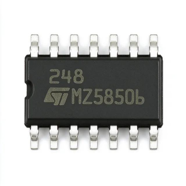
The STMicroelectronics LM248DT is a quad bipolar operational amplifier in a 14-pin SOIC package, providing four independent, high-gain, internally compensated amplifiers with characteristics similar to the UA741. The verified data identifies a 1.3 MHz gain-bandwidth product, 0.5 V/µs slew rate, 1 mV input offset voltage, 2 nA input offset current, 30 nA input bias current, and approximately 0.53 mA supply current per amplifier. The LM248DT is pin-compatible with the LM224 and LM324 families according to the manufacturer datasheet. An operational amplifier is an analog integrated circuit that uses high open-loop gain and negative feedback to amplify small voltage signals. A quad operational-amplifier package contains four amplifiers, allowing a design to implement four independent signal-processing channels while reducing board area and package count. Within the product hierarchy, the LM248DT is a bipolar operational amplifier, a general-purpose analog IC, and a member of the broader amplifier and signal-conditioning category. The LM248DT's Class AB output stage avoids crossover distortion, making it useful where low distortion is preferred over the lower output-current capability associated with CMOS amplifiers. Its internally compensated architecture simplifies closed-loop design without external compensation networks. Low input offset voltage supports precision-feedback applications, while the low input bias and offset currents reduce error in source impedances that are not extremely low. The four amplifiers operate independently, providing internal isolation between channels and allowing simultaneous use in unrelated circuit blocks. The 1.3 MHz gain-bandwidth product supports moderate-bandwidth signal amplification and active filtering, while the 0.5 V/µs slew rate is suitable for general-purpose waveform and feedback tasks. Because bipolar inputs can require more input-bias current than CMOS input amplifiers, source impedance and input-common-mode headroom should be checked against the manufacturer datasheet. Typical uses include industrial process-control loops, instrumentation amplifiers, sensor conditioning, active filters, transducers, and general-purpose analog signal chains. Four amplifiers in one package can be allocated to instrumentation stages, filters, and buffer functions. In designs requiring rail-to-rail input or output behavior, very low supply voltage, or rail-to-rail output drive, a modern precision CMOS amplifier may be more appropriate. When designing around the LM248DT, verify the supply-voltage range, input common-mode range, output swing, operating-temperature grade, and package pinout against the manufacturer datasheet. Decoupling capacitors should be placed close to the supply pins, and unused amplifier channels should be configured according to the datasheet rather than left floating. A common-mode input beyond the specified range can cause input-stage saturation and loss of normal operation. This page combines verified manufacturer and distributor information with pin-compatible alternatives, practical selection guidance, application analysis, and engineering design notes. It is intended to help engineers identify whether the LM248DT fits a legacy or new analog circuit without relying on undocumented assumptions about electrical limits, stock, or cross-references.

USD $0,95 Stokta
LM248N - Quad 36V 1MHz Op Amp | Texas Instruments
LM248N

LM248N - Quad 36V 1MHz Op Amp | Texas Instruments

The Texas Instruments LM248N is a quad, general-purpose operational amplifier with four independent high-gain amplifiers, a 36 V maximum supply rating, 1 MHz gain-bandwidth product, and a 14-pin PDIP package. The device operates from -25°C to 85°C and is designed for instrumentation, buffering, signal conditioning, and general-purpose analog applications. Its quad organization allows multiple amplifier sections to share one package while retaining independent operation. An operational amplifier is an analog integrated circuit that uses high open-loop gain to amplify the difference between its input voltages. The LM248 belongs to the broader hierarchy of operational amplifier, analog amplifier, and semiconductor devices. Unlike a comparator, the LM248 is intended for linear signal amplification, while its overload protection and internally compensated design support practical feedback-based circuit implementation. The LM248N combines a 1 MHz gain-bandwidth product with a slew rate of 0.5 V/µs, according to the verified product search results. Its input and output overload protection make it suitable for conventional op-amp stages connected to external resistors and feedback networks. The four independent circuits in the package can be assigned separately to instrumentation buffers, active filters, sensor interfaces, or voltage-feedback stages when circuit conditions meet the device requirements. The LM248N is identified by the verified search data as a standard general-purpose amplifier in a 14-PDIP package. The product family is also described as designed to be interchangeable with industry-standard LM148, LM248, and LM348 devices. The verified distributor listing identifies the part as a four-circuit amplifier, confirming the quad-channel architecture and through-hole package format. Typical applications include low-frequency analog signal conditioning, buffered sensor interfaces, audio and communications support circuits, general instrumentation, and multiple-channel analog systems. Because it is a bipolar-style general-purpose amplifier family, designers should verify supply voltage, input common-mode range, output swing, stability, and load conditions against the manufacturer datasheet before finalizing a design. The primary design consideration is to follow the manufacturer’s recommended supply, biasing, feedback, and decoupling arrangements. Because no complete electrical characteristic table or application-specific circuit constraints were included in the verified data, unsupported values are marked for engineering follow-up rather than inferred. This page summarizes verified product identity, architecture, package, and application context alongside sourcing and replacement guidance. This page synthesizes verified manufacturer and distributor information, drop-in replacement considerations, comparison fields, and practical engineering guidance for LM248N selection and PCB integration.

RFQ İletişim
LM2506SQ - 320 Mbps Pixel Link Serializer | Texas Instruments
LM2506SQ

LM2506SQ - 320 Mbps Pixel Link Serializer | Texas Instruments

Texas Instruments LM2506SQ is a 320 Mbps Low Power Mobile Pixel Link serializer/deserializer for 18-bit RGB display data, packaged in a 40-WQFN 5 x 5 mm surface-mount package. The device provides 22 serialized inputs and 3 deserialized outputs, linking a graphics source to a display panel over a compact differential interface. Its operating supply range is 2.5 V to 6.5 V, and the LM2506 family is designed for low-power mobile display systems. A Mobile Pixel Link serializer/deserializer is a display-interface IC that converts parallel pixel data into a high-speed serial link and reconstructs parallel data at the receiving endpoint. It belongs to the serializer/deserializer class within interface ICs and system-level display transport. The Mobile Pixel Link architecture reduces the number of PCB signal traces required between a graphics engine and display, which is especially useful where connector count, board area, EMI control, and power efficiency are important. The LM2506SQ supports data rates up to 320 Mbps and is intended for 18-bit RGB display interfaces. Its low-power design targets compact embedded and mobile equipment rather than general-purpose storage or networking links. The 40-WQFN package provides a dense surface-mount footprint, while the serializer/deserializer arrangement allows display data to be transmitted over fewer conductors than a conventional parallel RGB bus. Operation from 2.5 V to 6.5 V permits integration with common embedded display systems that use either 3.3 V or 5 V signaling environments. The manufacturer datasheet is the controlling document for timing, electrical limits, initialization, color mapping, and pin-level implementation. Engineers should treat the specified clocking, lane timing, power sequencing, and display timing values as mandatory constraints rather than infer them from the 320 Mbps headline rate. Typical uses include small-format LCD and OLED panels, portable instruments, industrial human-machine interfaces, automotive display modules, medical monitoring displays, and compact embedded systems. The LM2506SQ is most appropriate when both ends of the link can be configured for Mobile Pixel Link and when reduced trace count is more valuable than retaining a wide parallel RGB interface. A critical design step is verifying the complete panel-side connection, including supply sequencing, clock source, ground distribution, differential pair routing, and display timing initialization. Route high-speed links on a continuous reference plane, maintain the manufacturer-recommended spacing, and avoid introducing stubs or test-point discontinuities that can degrade signal integrity. This page combines the LM2506 interface characteristics, verified package and rate details, same-family replacement options, comparison parameters, and practical PCB guidance to support faster component selection and board design.

RFQ İletişim
LM258AD - Dual 30V 700kHz Op Amp | Texas Instruments
LM258AD

LM258AD - Dual 30V 700kHz Op Amp | Texas Instruments

The Texas Instruments LM258AD is a dual, internally frequency-compensated operational amplifier designed for low-power operation from a single supply. It combines a 30 V maximum supply rating, 700 kHz gain-bandwidth product, 1.1 MHz unity-gain bandwidth, and approximately 500 uA supply current per amplifier in an 8-pin SOIC package. The device provides two independent amplifiers in one package and operates over the -25°C to 85°C temperature range. An operational amplifier is an analog signal-conditioning IC that uses high open-loop gain to amplify the difference between voltages applied to its inverting and non-inverting inputs. The LM258AD belongs to the operational-amplifier family within the broader linear-amplifier and analog-signal-processing hierarchy. Its internally frequency-compensated architecture eliminates the need for an external compensation capacitor in typical closed-loop configurations. Key features include a large DC voltage gain of 100 dB, a 1.1 MHz unity-gain bandwidth, low input bias current of 20 nA, and supply current that remains essentially independent of supply-voltage magnitude. The two amplifiers can be used in non-inverting, inverting, comparator, summing, difference, and general feedback configurations. The single-supply capability also supports battery-powered and industrial signal-conditioning equipment. Each amplifier is intended for operation over a wide supply range, with the verified manufacturer description identifying a 30 V maximum supply voltage and a -25°C to 85°C operating-temperature range. Internal frequency compensation makes the device suitable for straightforward fixed-gain implementations without an additional compensation network. Engineers should still account for input common-mode limits, output swing, stability, input offset, and output-current limitations according to the manufacturer datasheet. Typical applications include transducer and sensor-signal conditioning, low-current industrial control, audio preamplification, bridge-amplifier interfaces, and power-supply feedback networks. The dual configuration saves board area when two low-frequency analog channels are required. Compared with a switching regulator or a modern rail-to-rail amplifier, the LM258AD prioritizes low quiescent current, wide supply-voltage headroom, and straightforward single-supply operation. When laying out the circuit, keep input and feedback paths short and place compensation or filtering capacitors close to their associated pins when required by the selected topology. Check output-current demand and input common-mode range against the actual supply voltage. Do not assume rail-to-rail input or output behavior; the available headroom and output swing are important constraints in low-voltage designs. This page consolidates the verified manufacturer specifications, distributor availability information, package details, and practical selection guidance. It also distinguishes pin-compatible alternatives from merely similar amplifiers and highlights missing electrical data explicitly rather than estimating values that are not established by the supplied sources.

RFQ İletişim
LM258ADGKR - Dual 30V 700kHz Op Amp | Texas Instruments
LM258ADGKR

LM258ADGKR - Dual 30V 700kHz Op Amp | Texas Instruments

The Texas Instruments LM258ADGKR is a dual, general-purpose operational amplifier rated for a maximum total supply voltage of 30 V, a typical gain-bandwidth product of 700 kHz, and a maximum input offset voltage of 3 mV. The device is packaged in an 8-pin VSSOP (DGK) and operates from -25°C to 85°C. An operational amplifier, or op amp, is an analog integrated circuit that amplifies the voltage difference between its inverting and non-inverting inputs. The LM258 belongs to the general-purpose amplifier family within the broader voltage-feedback amplifier hierarchy. Its frequency compensation is internal, allowing each channel to operate as a stable closed-loop amplifier without an external compensation capacitor. The two channels feature a typical slew rate of 0.3 V/µs, low supply-current drain of approximately 0.7 mA, and low input bias current. Each amplifier can operate from a single supply or from split supplies. The common-mode input range includes ground, which supports direct sensing of signals near the negative rail and makes the device useful in battery-powered monitoring circuits. Common applications include low-frequency sensor conditioning, transducer amplification, audio preamplification, analog signal filtering, and general control loops. Because the LM258ADGKR provides more supply-voltage headroom than many modern rail-to-rail amplifiers, it remains useful when signals exceed 12 V or when a single supply of 24 V must be accommodated. The output stage does not rail-to-rail swing, so output-headroom calculations are required at the chosen supply voltage. When designing a new board, use a 100 nF bypass capacitor close to each supply pin and verify output swing, load current, stability, and common-mode range at the actual signal amplitude. Confirm that the amplifier output remains above the lower saturation limit and below the upper load-dependent limit. This page combines manufacturer specifications, package details, drop-in replacement options, application guidance, and practical design notes to support component selection and PCB implementation.

RFQ İletişim
LM258ADR - Dual 30V 700kHz Op Amp | Texas Instruments (Tape & Reel)
LM258ADR

LM258ADR - Dual 30V 700kHz Op Amp | Texas Instruments (Tape & Reel)

The Texas Instruments LM258ADR is a dual, internally frequency-compensated operational amplifier designed for low-power operation from a single supply. It combines a 30 V maximum supply rating, 700 kHz gain-bandwidth product, 1.1 MHz unity-gain bandwidth, and approximately 500 uA supply current per amplifier in an 8-pin SOIC package. The device provides two independent amplifiers in one package and operates over the -25°C to 85°C temperature range. An operational amplifier is an analog signal-conditioning IC that uses high open-loop gain to amplify the difference between voltages applied to its inverting and non-inverting inputs. The LM258ADR belongs to the operational-amplifier family within the broader linear-amplifier and analog-signal-processing hierarchy. Its internally frequency-compensated architecture eliminates the need for an external compensation capacitor in typical closed-loop configurations. Key features include a large DC voltage gain of 100 dB, a 1.1 MHz unity-gain bandwidth, low input bias current of 20 nA, and supply current that remains essentially independent of supply-voltage magnitude. The two amplifiers can be used in non-inverting, inverting, comparator, summing, difference, and general feedback configurations. The single-supply capability also supports battery-powered and industrial signal-conditioning equipment. Each amplifier is intended for operation over a wide supply range, with the verified manufacturer description identifying a 30 V maximum supply voltage and a -25°C to 85°C operating-temperature range. Internal frequency compensation makes the device suitable for straightforward fixed-gain implementations without an additional compensation network. Engineers should still account for input common-mode limits, output swing, stability, input offset, and output-current limitations according to the manufacturer datasheet. Typical applications include transducer and sensor-signal conditioning, low-current industrial control, audio preamplification, bridge-amplifier interfaces, and power-supply feedback networks. The dual configuration saves board area when two low-frequency analog channels are required. Compared with a switching regulator or a modern rail-to-rail amplifier, the LM258ADR prioritizes low quiescent current, wide supply-voltage headroom, and straightforward single-supply operation. When laying out the circuit, keep input and feedback paths short and place compensation or filtering capacitors close to their associated pins when required by the selected topology. Check output-current demand and input common-mode range against the actual supply voltage. Do not assume rail-to-rail input or output behavior; the available headroom and output swing are important constraints in low-voltage designs. This page consolidates the verified manufacturer specifications, distributor availability information, package details, and practical selection guidance. It also distinguishes pin-compatible alternatives from merely similar amplifiers and highlights missing electrical data explicitly rather than estimating values that are not established by the supplied sources.

RFQ İletişim
LM258ADRE4 - Dual 700 kHz Op Amp in 8-SOIC | Texas Instruments
LM258ADRE4

LM258ADRE4 - Dual 700 kHz Op Amp in 8-SOIC | Texas Instruments

The Texas Instruments LM258ADRE4 is a dual general-purpose operational amplifier with two independent, internally frequency-compensated amplifiers, a 700 kHz gain-bandwidth product, and an 8-SOIC package. The device accepts single or split supplies, supports a 32 V maximum total supply voltage, and can operate with an input common-mode range that includes ground. These characteristics make it suitable for industrial control, instrumentation, sensor conditioning, and low-cost general-purpose analog signal paths. An operational amplifier is an analog integrated circuit that provides high open-loop gain and stable closed-loop behavior when connected with negative feedback. The LM258 belongs to the broader hierarchy of operational amplifier, voltage-feedback amplifier IC, analog IC, and semiconductor. Unlike rail-to-rail precision amplifiers, the LM258 relies on conventional bipolar input and output stages, making it appropriate where moderate input offset, output swing, and supply-current requirements are acceptable. Key features include two amplifier channels in one 8-SOIC package, internal frequency compensation, a typical gain-bandwidth product of 700 kHz, and operation from a single supply or split supplies. According to the manufacturer datasheet, the typical input offset voltage is 2 mV, typical input offset current is 2 nA, typical input bias current is 15 nA, and typical supply-current drain is 0.7 mA per amplifier. The common-mode input range includes ground, which is useful for sensing signals near the lower supply rail. The LM258AD uses two internal voltage-compensated amplifiers designed for general-purpose operation. Internal compensation removes the need for an external dominant-pole capacitor in typical closed-loop configurations. Because the amplifier is not rail-to-rail at its inputs or outputs, output-headroom and common-mode calculations must be completed for the actual supply voltage, load current, output waveform, and connected feedback network. Typical uses include low-side current measurement, sensor amplification, buffered references, audio and communications interfaces, and industrial analog modules. Its 700 kHz bandwidth supports moderate-frequency feedback loops, while the dual-channel arrangement reduces component count when two independent amplifier functions are required. PCB design should prioritize short feedback traces, clean grounding, and decoupling close to the supply pins. Place the supply-bypass capacitor between the V+ and ground connections at the device, keep high-impedance input nodes away from switching-current paths, and verify common-mode and output-swing margins across the full operating range. This page combines package and electrical characteristics with drop-in replacement guidance, application-specific engineering notes, and a parameter-by-parameter comparison. It also highlights verification points for supply voltage, temperature grade, pin compatibility, and manufacturer qualification before a component is approved for production.

RFQ İletişim
LM258ADRG4 - Dual 30V 700kHz Op Amp | Texas Instruments
LM258ADRG4

LM258ADRG4 - Dual 30V 700kHz Op Amp | Texas Instruments

The Texas Instruments LM258ADRG4 is a dual general-purpose operational amplifier with a 700 kHz gain-bandwidth product, 0.3 V/µs slew rate, 3 mV typical input offset voltage, and operation across a -25°C to 85°C temperature range. Each amplifier supports supply voltages from ±1.5 V to ±16 V, and the device is packaged in an 8-pin SOIC (D). The LM258ADRG4 suffix identifies the tape-and-reel ordering option. An operational amplifier is an analog amplifier that uses very high open-loop gain to amplify the difference between two input voltages. The LM258A belongs to the operational-amplifier hierarchy, which includes general-purpose amplifiers, precision amplifiers, instrumentation amplifiers, and comparators. Its two independently compensated channels can implement buffer, gain, summing, active-filter, transducer, and feedback-control circuits from a single or split power supply. The headline features are 700 kHz bandwidth, 0.3 V/µs slew rate, and ±1.5 V to ±16 V operating range. Typical input offset voltage is 3 mV, while typical input offset current is 2 nA and typical input bias current is 15 nA. The common-mode input range includes ground, making the device useful for circuits that process low-level signals close to the negative supply rail. Internal frequency compensation removes the need for an external compensation network. Internally, the LM258A uses two frequency-compensated amplifier sections optimized for general-purpose signal conditioning. Its moderate bandwidth supports audio and control applications without requiring the speed or precision of a dedicated high-voltage amplifier. The architecture is intended for broad supply-voltage operation, useful in industrial equipment powered from unregulated rails and in split-supply analog circuits. The maximum-rated differential input range is 32 V, subject to the device's absolute maximum conditions. Typical applications include low-level sensor signal conditioning, active filtering, audio preamplification, relay and actuator drive interfaces, power-supply feedback, and dual-channel industrial control loops. Using one package for two channels can also reduce board area when both channels require similar common-mode and supply characteristics. The operating-temperature grade supports commercial and industrial ambient conditions rather than the full automotive temperature range. Design should preserve adequate input and output voltage headroom, account for offset when sensing near ground, and place input-referenced error sources close to the amplifier. Decoupling capacitors should be placed directly across the supply pins, while sensitive feedback nodes require short traces and careful grounding. Verify source and sink current capability against the intended load because a wide supply range alone does not guarantee adequate output-current margin. This page combines the Texas Instruments product specifications, package and pin information, sourcing guidance, engineering design notes, and a pin-compatible comparison with other dual operational amplifiers. It is intended to accelerate component selection, PCB planning, and replacement assessment for engineers working with the LM258ADRG4 in 8-pin SOIC designs.

RFQ İletişim
LM258AH - Dual 30V Low-Power Op Amp | STMicroelectronics
LM258AH

LM258AH - Dual 30V Low-Power Op Amp | STMicroelectronics

STMicroelectronics LM258AH is a dual, low-power operational amplifier designed for single-supply operation over a wide voltage range, with two independent, internally frequency-compensated amplifiers in an 8-lead TO-99-8 metal package. The LM258 family supports input voltages up to 30 V, operating frequency up to 700 kHz, and an industrial ambient-temperature range of -25 °C to +85 °C. The LM258AH ordering suffix identifies the wire-lead TO-99-8 industrial-temperature configuration. An operational amplifier, or op amp, is a high-gain analog building block used to amplify small voltage signals. Within the wider semiconductor hierarchy, the LM258AH is an analog integrated circuit and a dual operational amplifier. Its two independent channels can support signal conditioning, feedback control, voltage comparison, and general-purpose analog amplification without requiring a split-supply arrangement. The key features of the LM258AH include two amplifiers in one package, internal frequency compensation, and a maximum input voltage of 30 V. The LM258 family is designed around a 700 kHz gain-bandwidth characteristic, while the LM258A version has an input offset voltage specified as 3 mV by the cited manufacturer information. The low-power architecture is intended for applications that require wider supply-voltage tolerance than conventional low-voltage single-supply op amps. The internally compensated architecture simplifies closed-loop amplifier design because it avoids the external compensation components normally required by higher-gain parts. Independent channels may also be used for unrelated signal paths, although common supply pins mean both channels share the same operating rail and thermal environment. Designers should still verify output swing, input common-mode range, output-current capability, and stability against their actual source and load impedances. Typical uses include industrial process-control loops, sensor-signal conditioning, low-frequency filter stages, comparators, and general analog signal chains. The wide operating-voltage capability can simplify legacy and industrial designs that operate from higher single rails. The 700 kHz bandwidth is appropriate for low-frequency precision and control tasks, but it is generally not the preferred choice for high-speed video, RF, or wideband data-acquisition requirements. The principal design considerations are supply decoupling, input common-mode limits, output swing, and thermal behavior. Place the supply bypass capacitor close to the device and avoid driving outputs into hard clamps except where the application intentionally requires saturation. Verify the complete circuit against the STMicroelectronics LM258 datasheet, particularly for AC output current, noise, offset voltage, and load-capacitance stability. This product page consolidates the verified manufacturer and distributor information for the LM258AH and distinguishes the TO-99-8 metal-package option from surface-mount and other package variants. It also provides compatibility-focused replacement guidance, practical circuit considerations, and a specification comparison structured around engineers evaluating an existing TO-99-8 dual-op-amp design.

RFQ İletişim
LM258AM - Dual 30V 700kHz Operational Amplifier | onsemi
LM258AM

LM258AM - Dual 30V 700kHz Operational Amplifier | onsemi

onsemi LM258AM is a dual general-purpose operational amplifier designed for single-supply operation, with two independent, internally frequency-compensated amplifiers in an 8-pin SOIC package. The device supports input voltages up to 30 V, operates across the -25°C to +85°C temperature range, and features a 700 kHz gain-bandwidth product. Its dual-channel configuration allows one package to implement two amplification, filtering, comparison, or signal-conditioning functions. An operational amplifier is a high-gain analog signal-processing IC that compares its inverting and non-inverting inputs and drives its output according to the voltage difference between them. The LM258 family belongs to the operational-amplifier category within analog amplifiers and linear integrated circuits. It is intended for general-purpose designs rather than precision, low-noise, or high-speed instrumentation, providing a practical balance of supply range, gain, common-mode capability, and output swing. Key features include two independent channels, large DC voltage gain of 100 dB, and internal frequency compensation that supports unity-gain operation without an external compensation network. The input common-mode voltage range includes ground, supporting single-supply signal conditioning where the signal is referenced to 0 V. These characteristics make the LM258AM suitable for transducers, industrial controls, audio and communication interfaces, sensor amplification, and general feedback-control circuits. The architecture is based on two independent high-gain amplifier sections with internal compensation. Internal compensation simplifies PCB design and improves usability at unity gain, while the wide supply range permits operation from lower-voltage single supplies through industrial supplies up to 30 V. Because this is a general-purpose bipolar-style amplifier family, engineers should verify input common-mode limits, output swing, load capability, stability, and supply-current requirements against the manufacturer datasheet for the exact operating conditions. Typical applications include current-loop and voltage-feedback control, low-side sensing, sensor signal conditioning, audio preamplification, active filtering, threshold detection, and general industrial interface circuits. The dual arrangement is especially useful when a design needs two related functions, such as an error amplifier paired with a buffer or a comparator paired with a gain stage. When laying out an LM258AM circuit, keep input and feedback connections compact to minimize parasitic pickup, provide adequate supply bypassing near the device, and verify that source and load impedances remain within the stability requirements of the internal compensation. The SOIC-8 package also allows a smaller footprint than a traditional through-hole dual operational amplifier. This page consolidates the LM258AM electrical characteristics, package information, verified source links, replacement considerations, comparison parameters, and practical design guidance into one engineering-focused resource for part selection and PCB implementation.

RFQ İletişim
LM258AMX - Dual 3-32V Op Amp | onsemi | 8-SOIC
LM258AMX

LM258AMX - Dual 3-32V Op Amp | onsemi | 8-SOIC

The onsemi LM258AMX is a dual, internally frequency-compensated operational amplifier designed for single-supply operation over a wide voltage range. The device contains two independent high-gain amplifiers in an 8-pin SOIC package. According to the Fairchild Semiconductor LM258A family documentation, the LM258A series supports a 3 V to 32 V power supply range, provides large DC voltage gain of 100 dB, and includes an input common-mode voltage range that reaches ground. The amplifiers are optimized for general-purpose signal conditioning, instrumentation, buffering, and feedback control. An operational amplifier is an active analog signal-processing component that uses differential input voltage to control an output voltage. A dual operational amplifier combines two amplifiers in one package, reducing board area and simplifying power-supply routing. The LM258AMX combines this general-purpose amplifier function with internal frequency compensation, allowing stable operation at unity gain without an external compensation capacitor. This makes it useful in designs where the signal source does not require a specialized low-noise or high-speed amplifier. The main electrical features of the LM258A family include internal frequency compensation for unity gain, 100 dB large DC voltage gain, and a wide power-supply range. The input common-mode voltage range includes ground, which permits the amplifier to process signals close to the lower supply rail. The output swing is characterized as extending to VCC minus 1.5 V, a relevant consideration when the amplifier must drive an ADC, a relay driver, or another circuit with limited headroom. The 8-SOIC package is a standard surface-mount format suitable for conventional PCB assembly. Typical uses include current sensing in industrial control equipment, signal conditioning in sensor interfaces, audio preamplifier stages, feedback networks in power converters, and general instrumentation. In a current-sense amplifier, the two independent channels can monitor different loads or provide differential amplification stages. In a sensor interface, the input common-mode range can simplify conditioning of signals referenced to ground. Designers should still account for the output-voltage headroom, supply decoupling, input bias currents, and the frequency-response limits of the selected amplifier configuration. The LM258AMX is appropriate when a design needs two amplifiers, a broad single-supply operating range, and a familiar 8-pin SOIC footprint. It is less suitable for applications requiring very low noise, rail-to-rail input or output operation, high slew rate, or precision offset and drift performance. This page combines the manufacturer-family electrical characteristics with package information, application guidance, and practical design considerations for evaluating the part in new analog circuits.

RFQ İletişim
LM258AN - Dual Low-Power Op Amp | STMicroelectronics
LM258AN

LM258AN - Dual Low-Power Op Amp | STMicroelectronics

STMicroelectronics LM258AN is a low-power dual operational amplifier containing two independent, high-gain, internally frequency-compensated amplifiers. It is packaged in an 8-pin Mini DIP and is designed for single-supply operation over a wide voltage range. Each channel is internally compensated for unity-gain stability, allowing operation without an external frequency-compensation network. An operational amplifier, or op amp, is a voltage-gain amplifier that compares an inverting input with a non-inverting input and drives its output toward the difference between them. The LM258 belongs to the broader linear-IC hierarchy: operational amplifier, analog amplifier, voltage amplifier, and semiconductor. Internally compensated dual op amps are useful when a board needs two independent amplifier channels while limiting component count and keeping the two channels in one package. The LM258AN provides two amplifier circuits with a large DC voltage gain of 100 dB and unity-gain frequency compensation. Its input common-mode voltage range includes ground, an important characteristic for circuits powered from a single positive supply and biased near the lower supply rail. The low-power architecture is designed to maintain low supply drain independently of the magnitude of the supply voltage, according to the manufacturer family documentation. Each amplifier channel has separate input and output pins, while the two channels share the power supply connections. This arrangement supports conventional non-inverting, inverting, voltage follower, summing, and differential signal-conditioning circuits. Because the amplifiers are internally compensated, stable unity-gain operation can be implemented with a minimum external feedback network, reducing design effort in general-purpose analog equipment. Typical LM258AN applications include sensor-signal conditioning, industrial control loops, low-frequency active filters, relay-driver interfaces, audio preamplifier stages, and buffered measurement systems. The dual configuration is especially useful when a circuit requires two related analog channels, such as an instrumentation amplifier input stage, motor-control feedback network, or dual-channel sensor interface. When designing around the LM258AN, verify the exact input common-mode range, output swing, supply-current limits, and operating-temperature limits for the LM258 variant against the STMicroelectronics datasheet. Decoupling capacitors should be placed close to the supply pins, and the feedback network should preserve stable operation at the intended signal frequency. This product page combines the LM258AN family characteristics, package information, sourcing guidance, comparison parameters, and practical circuit-planning notes. It is intended to help engineers evaluate the device for single-supply analog designs and identify same-package alternatives without overlooking package or qualification differences.

RFQ İletişim
LM258AP - Dual 30V 700kHz Op Amp | Texas Instruments
LM258AP

LM258AP - Dual 30V 700kHz Op Amp | Texas Instruments

Texas Instruments LM258AP is a dual, general-purpose operational amplifier supplied in an 8-pin PDIP package. It supports operation from a single supply or split supply over a wide voltage range, with a maximum total supply voltage of 32 V. The LM258 family provides 700 kHz gain-bandwidth product, 0.3 V/µs slew rate, and approximately 3 mV input offset voltage for the LM258A version, making it suitable for conventional analog signal conditioning. An operational amplifier is an analog semiconductor that amplifies the voltage difference between its two inputs. Its applications include voltage buffers, current-to-voltage conversion, active filters, comparators, instrumentation circuits, and low-frequency closed-loop control. The dual LM258 architecture provides two amplifiers in one package, reducing board area in designs that need independent or complementary analog channels. The LM258A operating-temperature range extends from -25°C to 85°C. The principal characteristics are a 700 kHz typical gain-bandwidth product, 0.3 V/µs slew rate, and 3 mV offset voltage for LM258A. The device operates with total supply voltages from 3 V to 32 V, including single-supply configurations near 3 V and split supplies up to approximately ±16 V. Its 8-pin PDIP package also facilitates prototyping and through-hole assembly where leaded components are preferred. LM258 devices are internally frequency-compensated dual operational amplifiers. Internal compensation allows operation as unity-gain voltage followers without external compensation components, which simplifies many basic amplifier layouts. Users must still observe input common-mode and output-swing limits, maintain the specified supply voltage, and use adequate bypassing to prevent oscillation or unexpected analog noise. The dual configuration also permits one channel to perform signal amplification while the other handles a separate task. Typical uses include low-frequency active filters, DC sensor amplification, industrial control-signal conditioning, audio preamplifier stages, comparators, and general instrumentation. In a basic non-inverting stage, the closed-loop gain is established by the feedback network, while the amplifier provides high input impedance and low output impedance. In a transimpedance stage, the feedback resistor converts input current into a voltage, making the LM258 suitable for photodiode and detector interfaces when operating within its bandwidth and dynamic-range limits. A critical design consideration is to place the specified bypass capacitor close to the supply pins and route feedback components to minimize parasitic capacitance and oscillation risk. Check common-mode input range, output swing, load capability, and thermal dissipation at the actual supply voltage. Keep sensitive input nodes away from switching-current paths and use a stable ground reference to reduce offset and noise pickup. This product page combines manufacturer specifications, package details, drop-in alternatives, application guidance, and design considerations for engineers evaluating the LM258AP. It also distinguishes verified electrical parameters from parameters that require design confirmation, helping teams plan analog prototypes, production PCB layouts, and replacement decisions with fewer assumption-driven errors.

RFQ İletişim
LM258AWDT - Dual 30V Low-Power Op Amp | STMicroelectronics
LM258AWDT

LM258AWDT - Dual 30V Low-Power Op Amp | STMicroelectronics

The STMicroelectronics LM258AWDT is a dual general-purpose operational amplifier designed for low-power operation from a single 3 V to 30 V supply. It provides two amplifier channels in an 8-pin SOIC package, with input and output voltage ranges extending to ±1.5 V and ±15 V, respectively. Key characteristics include 1.1 MHz gain-bandwidth product, 0.6 V/µs slew rate, 20 nA input bias current, and up to 60 mA of output current per channel. The LM258AWDT is supplied in tape-and-reel packaging for automated assembly. A general-purpose operational amplifier is an analog signal-conditioning IC that uses differential feedback to amplify a voltage difference. In the broader electronics hierarchy, an operational amplifier belongs to the amplifier IC and signal-conditioning categories, where it supports sensor interfaces, buffer stages, error amplifiers, analog-to-digital converter drivers, and general feedback-control circuits. The LM258 family combines broad supply-voltage tolerance with low quiescent-current operation, making it useful where the signal level and supply voltage vary across industrial or automotive equipment. The principal features of the LM258AWDT include two independent channels, a 3 V to 30 V operating range, 85 dB open-loop gain-bandwidth behavior, low 20 nA input bias current, and approximately 0.1 µA input offset current. Its 1.1 MHz gain-bandwidth product supports moderate-frequency signal amplification, while the 0.6 V/µs slew rate supports reasonably clean output transitions. A 60 mA per-channel output-current capability is useful for driving moderate loads and providing isolation between high-impedance sources and downstream circuitry. The automotive “A” version is identified as AEC-Q100 qualified in the available component information. This qualification is meaningful in applications where operating temperature, shock, vibration, and extended-life reliability require controlled automotive qualification. Because it is a bipolar, low-power dual op amp, the LM258AWDT emphasizes supply flexibility and input-current behavior rather than rail-to-rail input or output operation. Its usable common-mode and output ranges therefore need to remain inside the limits specified by the manufacturer datasheet. Typical applications include industrial sensor conditioning, battery-powered instrumentation, current-loop receivers, analog signal buffers, bridge-amplifier interfaces, and low-frequency control loops. Automotive electronics can use the qualified version where its operating and environmental ratings match the system requirements. Two channels can be used independently or together for differential, summing, instrumentation, or active-filter configurations, reducing the number of separate amplifier packages required on a board. The main design consideration is rail-to-rail behavior. A circuit requiring input or output swing close to either supply rail may not be served by the LM258AWDT’s conventional common-mode range. Designers should also check output-current limits, load capacitance, supply ripple, feedback stability, and the minimum operating voltage for the selected gain configuration before finalizing the circuit. This page combines the LM258AWDT’s principal electrical ratings, automotive qualification, package details, practical applications, same-footprint alternatives, and design guidance to support component selection, PCB planning, sourcing, and schematic review.

RFQ İletişim
LM258AWYPT - Dual 30V Low-Power Op Amp | STMicroelectronics
LM258AWYPT

LM258AWYPT - Dual 30V Low-Power Op Amp | STMicroelectronics

The STMicroelectronics LM258AWYPT is a dual, general-purpose operational amplifier with two independent amplifiers, a 1.1 MHz gain-bandwidth product, and a 3 V to 30 V supply-voltage range in an 8-pin TSSOP package. Its low-power design is intended for industrial control, sensor conditioning, and general analog signal-chain applications. An operational amplifier is an analog integrated circuit that amplifies the difference between two input voltages. When negative feedback is applied, the device creates a closed-loop gain determined mainly by external resistors. The operational-amplifier category belongs to the amplifier IC hierarchy, which includes instrumentation, precision, and general-purpose amplifiers used for signal conditioning, control, and system-level analog processing. The LM258AWYPT provides two amplifiers in one compact package. Key electrical characteristics include a 1.1 MHz gain-bandwidth product, 600 V/ms slew rate, 55 nV/√Hz noise density at 1 kHz, 85 dB common-mode rejection, and a 700 µA quiescent-current figure. Its operating temperature range of -40°C to +105°C supports industrial environments where consumer-grade amplifiers may be unsuitable. Each amplifier is internally frequency compensated, allowing stable operation without an external compensation capacitor in the standard closed-loop configurations. The device supports single-supply operation from 3 V to 30 V and dual-supply operation when the mid-supply reference is established appropriately. Its low quiescent current helps limit power consumption in battery-powered and distributed sensing systems. Typical applications include low-side current measurement, transducer conditioning, industrial sensor interfaces, feedback networks in power-control circuits, audio preamplification, and general buffered analog stages. Two independent amplifiers in one package can also implement a differential amplifier or instrumentation-style front end when suitable resistor networks and component tolerances are used. For PCB design, keep feedback resistors close to the associated input pins and maintain a low-impedance return path for each amplifier. Avoid long traces between the two amplifier channels when they carry different signals. Confirm output swing, common-mode range, stability, and input protection under the worst-case supply and load conditions before production release. This product page consolidates the LM258AWYPT electrical characteristics, verified package information, sourcing options, pin mapping, and practical guidance for engineers evaluating this low-power dual operational amplifier.

RFQ İletişim
LM258AYDT - Dual 1.1MHz Low-Power Op Amp | STMicroelectronics
LM258AYDT

LM258AYDT - Dual 1.1MHz Low-Power Op Amp | STMicroelectronics

STMicroelectronics LM258AYDT is a dual, general-purpose operational amplifier with a 1.1 MHz gain-bandwidth product and low-power characteristics, supplied in an 8-pin SOIC package. The device contains two independent amplifiers, making it suitable for signal conditioning, feedback control, filtering, sensing, and general dual-amplifier signal paths. An operational amplifier is an analog integrated circuit that uses high open-loop gain to amplify the difference between signals applied to its inverting and non-inverting inputs. The LM258AYDT belongs to the operational-amplifier hierarchy, combining low-power operation, dual-channel integration, and an 8-pin SOIC footprint in a component intended for cost-sensitive analog signal-chain designs. Key characteristics include two amplifier circuits in one package, a 1.1 MHz gain-bandwidth product, and low-power operation. The integrated dual configuration reduces external component count and PCB area when a design requires two matched-function amplifier channels. Its standard SOIC-8 package also supports conventional surface-mount assembly and hand-soldering or automated placement. The amplifier architecture is suited to closed-loop configurations in which feedback defines the gain and bandwidth. Designers must maintain the input common-mode voltage and output-voltage limits published by STMicroelectronics, because operation outside those limits can impair signal integrity or reduce reliability. Input and output stability should be evaluated using the manufacturer’s recommended source, load, and bypass-capacitor arrangements. Typical uses include industrial sensor interfaces, audio preamplifier stages, loop filters, sensor-conditioning channels, and low-frequency control or measurement circuits. Two amplifiers can implement differential, instrumentation-style signal handling, cascaded gain stages, active filters, or independent channels where board area is constrained. For PCB implementation, place decoupling capacitors close to the supply pins and route sensitive input and feedback paths away from high-current switching nodes. Check input bias-current effects, output swing, stability with the selected load, and the operating-temperature range before committing the design to production. This product page combines package, technical, replacement, and application guidance with practical design considerations. It also identifies where pinout, compliance, and detailed electrical values must be confirmed against the manufacturer’s LM258AYDT datasheet before layout release or component substitution.

RFQ İletişim
LM258AYPT - Dual Low-Power Op Amp, 8-TSSOP | STMicroelectronics
LM258AYPT

LM258AYPT - Dual Low-Power Op Amp, 8-TSSOP | STMicroelectronics

The STMicroelectronics LM258AYPT is a dual, low-power general-purpose operational amplifier packaged in an 8-pin TSSOP. It provides two independent amplifier channels, a listed gain-bandwidth product of 1.1 MHz and a listed DC gain of 100 dB, making it suitable for industrial control, sensor amplification, buffer, and general analog signal-conditioning circuits. An operational amplifier, commonly abbreviated op amp, is a high-gain analog building block that compares a differential input against a feedback-defined reference voltage. The LM258AYPT belongs to the dual low-power operational-amplifier family within the broader hierarchy of analog amplifiers, linear amplifiers, and integrated analog circuits. Its two channels can amplify independent signals or be combined in differential, filtering, instrumentation, and feedback-control topologies. The principal device characteristics include two amplifier circuits per package, an 8-TSSOP surface-mount form factor, 1.1 MHz gain-bandwidth product, and 100 dB listed gain. The compact package allows dual-channel designs to occupy less board area than two separate single-amplifier packages. Its low-power designation makes it appropriate for battery-operated instruments, industrial transducers, control systems, and power-conscious analog interfaces. Because the LM258 family is intended for general-purpose operation, engineers commonly select it for audio-frequency signal conditioning, current monitoring, sensor buffers, active filtering, and low-to-moderate-frequency feedback loops. The manufacturer datasheet is the controlling document for input common-mode range, output swing, output current, supply current, noise, stability requirements, and recommended external components. Designers should verify those limits against the actual supply voltage and signal amplitude before finalizing a high-impedance or capacitive-load design. Typical installations place one amplifier in a feedback stage and the other in a matching buffer, gain stage, or comparator-style threshold circuit. Decoupling capacitors should be placed close to the supply pins, and sensitive input traces should be kept away from switching nodes. The dual format is particularly useful when a system requires symmetric analog channels, such as differential sensing, bridge-amplifier interfaces, or dual-axis transducer conditioning. A key design trade-off is that a general-purpose amplifier may not provide rail-to-rail input or output operation. Confirm the usable input range and output swing against the chosen supply, especially in single-supply systems whose signals remain close to ground. Confirm stability with capacitive loads and validate noise, offset, and bandwidth requirements before committing to production quantities. This page combines package, pricing, sourcing, replacement, and design guidance for LM258AYPT. It organizes the practical considerations engineers need when comparing this TSSOP dual amplifier with related STMicroelectronics devices and when planning board layout, supply bypassing, signal conditioning, and lifecycle sourcing.

RFQ İletişim
LM258D - Dual 30V Operational Amplifier | STMicroelectronics
LM258D

LM258D - Dual 30V Operational Amplifier | STMicroelectronics

The STMicroelectronics LM258D is a dual, internally frequency-compensated operational-amplifier IC with two independent amplifiers, a 30 V maximum supply rating and a 700 kHz gain-bandwidth product. Each amplifier is designed for general-purpose signal conditioning from single or split supplies. The device is packaged for surface mounting in an 8-pin SOIC and is identified by the DigiKey listing as a standard, general-purpose, two-circuit amplifier. The supplied source data confirms the 30 V and 700 kHz headline ratings through Texas Instruments’ LM258 family page, but it does not provide a complete STMicroelectronics parameter table. An operational amplifier is a voltage-gain element that uses external feedback to control closed-loop behavior. The LM258D belongs to the dual operational-amplifier hierarchy and contains two independent amplifiers in one package. Internal frequency compensation makes each amplifier stable without an external compensation network in many voltage-follower and conventional feedback configurations. Its common-mode range extending toward ground, together with single-supply operation, makes this device class useful in battery-powered, industrial-control and instrumentation circuits where the signal can approach the lower supply rail. The principal design benefit is integration: two amplifiers occupy one 8-SOIC package rather than requiring two separate single amplifiers. Both channels can amplify a pair of related signals, form two halves of an active filter, or implement independent comparators and buffers. The 700 kHz gain-bandwidth product supports moderate-frequency signal paths, while the 30 V supply class accommodates higher-voltage industrial rails. Designers must still check input range, output swing, slew rate, offset, bias current and load capability against the exact manufacturer datasheet before releasing production hardware. Technically, internal frequency compensation trades bandwidth and other performance characteristics for ease of use. Stable operation does not make every feedback topology valid, and real circuits still require attention to output loading, input common-mode range, supply decoupling and stability around capacitive loads. Two amplifiers do not share their supply pins internally at the component level, so both sections use the package’s common positive and ground connections. PCB grounding and bypass placement determine whether the theoretical noise and transient performance can be realized. Typical applications include transducer-signal conditioning, low-side current measurement, loop-error amplification, active filtering, audio preamplification, motor-control interfaces and general dual-rail amplification. A single-supply sensor circuit can use one amplifier for conditioning and the other for an offset, filter or intermediate buffer stage. Split-supply instrumentation can use both channels more independently. Compared with modern low-voltage rail-to-rail amplifiers, the LM258D trades compactness and precision for its wide-supply capability and straightforward general-purpose use. When designing around the LM258D, place the supply bypass capacitor close to the IC and route each amplifier’s inputs and outputs to minimize leakage and feedback-loop pickup. Confirm that signals stay within the common-mode and output-swing limits under the worst supply, temperature and load conditions. Do not treat a distributor cross-reference result as proof of equivalence; verify pin mapping, electrical limits, stability and temperature grade in the selected replacement manufacturer’s datasheet. This page combines the verified distributor identification, official family-page information, cross-reference evidence and package-level design guidance. It distinguishes confirmed facts from parameters that were not supplied, avoiding invented precision while helping engineers evaluate LM258D procurement, replacement and circuit-integration decisions.

RFQ İletişim