Arayüz IC'leri
Alt Kategoriler
Ürünler (320+)

ISO6442 - Quad-Channel Digital Isolator 150Mbps | Texas Instruments
The Texas Instruments ISO6442 is a robust EMC, general-purpose quad-channel digital isolator with a 2/2 channel configuration (two forward, two reverse channels), supporting data rates up to 150 Mbps and a common-mode transient immunity (CMTI) of up to 250 kV/us. It is available in a 16-pin wide-body SOIC (DWR, 5000 Vrms reinforced isolation) and a 16-pin SSOP (DBQ, 3000 Vrms basic isolation). A digital isolator is a component that transfers digital signals across a galvanic isolation barrier, blocking high voltages, isolating ground potentials, and preventing noise currents between two sides of a circuit. Within the interface-IC hierarchy, digital isolators sit between logic controllers and high-voltage or noisy domains such as motor drives, inverters, and fieldbus networks. The ISO6442 belongs to TI's ISO644x family of basic and reinforced quad-channel isolators built on a proprietary capacitive isolation architecture using an SiO2 dielectric barrier. Key features include the wide 2.25 V to 5.5 V supply range on both sides, enabling direct interfacing with 1.8 V, 2.5 V, 3.3 V, and 5 V logic; a fail-safe default output of high for the standard ISO6442 during input power or signal loss (the ISO6442F defaults low); and robust EMC performance for harsh industrial noise environments. The reinforced DWR package supports sustained working-voltage isolation requirements. Architecturally, the device modulates the input signal across the capacitive barrier and reconstructs it at the output, delivering low power, high speed, and stable propagation characteristics over temperature and supply variation. Enable pins provide tri-state output control for power management and multipoint bus applications. Typical applications include isolated SPI interfaces, industrial fieldbus communication, motor drives, power inverters, battery management systems, and on-board chargers, where 150 Mbps throughput and 250 kV/us CMTI maintain signal integrity in electrically noisy conditions. When designing, maintain adequate creepage and clearance on the PCB, place 0.1 uF bypass capacitors close to both VCC pins, and verify that propagation delay and pulse-width distortion near 150 Mbps meet the timing requirements of the receiving peripheral.

ISO6442-Q1 - 150Mbps Quad-Channel Digital Isolator | TI
The Texas Instruments ISO6442-Q1 is an automotive-grade quad-channel digital isolator providing two forward and two reverse channels, a data rate up to 150 Mbps, and a common-mode transient immunity (CMTI) of 250 kV/us. The device is qualified to AEC-Q100 for automotive use and is available in reinforced and basic isolation ratings, with the ISO6442DBQRQ1 ordering option packaged in a 16-pin SSOP (DBQ) rated 3000 Vrms. A digital isolator is an integrated circuit that transmits digital signals across a galvanic isolation barrier, blocking high voltages, ground loops, and common-mode noise while passing logic data. Within the interface-IC hierarchy, digital isolators sit between a controller and noisy or high-voltage circuitry, complementing isolated transceivers, gate drivers, and isolated ADCs in systems requiring safety and signal integrity. Key features include the 250 kV/us CMTI, which keeps outputs correct in high-dv/dt environments such as motor-drive inverter legs, and the 150 Mbps data rate supporting fast SPI and parallel logic links. Enable pins allow each direction to be tri-stated for power management. In the event of input power or signal loss, default outputs are high; the ISO6442F-Q1 variant defaults low, giving designers a choice of fail-safe behavior. The ISO6442-Q1 uses TI's proven capacitive isolation technology, delivering robust EMC performance and long-term barrier reliability. The ISO644x-Q1 family (ISO6440/6441/6442 and F variants) shares package options including the DW-16 wide SOIC, DFP-16 wide SSOP, and DBQ-16 SSOP; a Functional Safety FIT rate and pin FMA document (SFFSB42) is available. Typical applications include EV battery management systems, isolated SPI links to current and voltage monitors, motor drives and inverters, and industrial fieldbus isolation. For reliable design, keep copper under the isolation barrier clear, decouple both VCC pins closely, and select the F-suffix variant when a low default output is required for safe power-loss behavior.

ISO6763 - 6-Ch Reinforced Digital Isolator 50Mbps | Texas Instruments
The Texas Instruments ISO6763 is a general-purpose six-channel (3/3 channel direction) reinforced digital isolator supporting data rates up to 50 Mbps with 5000 Vrms galvanic isolation in a 16-pin SOIC (DW, 7.50 mm width) package. It provides robust common-mode transient immunity of 50 kV/us and supports 1.8 V, 2.5 V, 3.3 V, and 5 V logic levels on both sides of the isolation barrier. A digital isolator is an interface IC that transfers digital signals across a galvanic isolation barrier while blocking high voltages, isolating ground potentials, and preventing noise coupling. Within the signal-chain hierarchy, digital isolators belong to the interface IC family and are essential building blocks in industrial data buses, isolated power supplies, and motor-drive gate-drive isolation systems. Key features include six isolation channels in a 3/3 configuration, 50 Mbps signaling for high-speed SPI and parallel interfaces, and reinforced 5000 Vrms isolation rating for safety-critical designs. The ISO6763 belongs to the ISO676x family (ISO6760, ISO6761, ISO6762, ISO6763, datasheet SLLSFK0E, August 2021, revised February 2023), which shares silicon-on-insulator-based capacitive isolation technology with the proven ISO77xx generation. The device uses TI's latest generation of capacitive isolation architecture with on-chip transformers implemented as SiO2 capacitors, delivering robust EMC performance with high CMTI. Low propagation delay and low channel-to-channel skew make it well suited for clocked interfaces. Wide-side supply support down to 1.8 V allows direct interfacing with modern low-voltage MCUs and FPGAs without level shifting. Typical applications include RS-485 and CAN bus isolation, isolated SPI for ADCs and DACs, industrial PLC I/O modules, and motor-control signal isolation connecting MCUs to gate drivers. The automotive-grade ISO6763FQDWRQ1 variant extends usage to vehicle systems requiring AEC-Q100 qualification. When designing, place 0.1 uF bypass capacitors close to both VCC1 and VCC2 pins and route signals across the barrier with generous creepage clearance; unused inputs should be tied to a defined logic level to prevent floating-channel oscillation.

ISO7321CDR - 25Mbps 2CH 3000Vrms Digital Isolator | Texas Instruments
The Texas Instruments ISO7321CDR is a low-power, dual-channel, 1/1 digital isolator delivering 25 Mbps signaling rate, 3000 Vrms galvanic isolation (1 minute per UL, 4242 Vpk per VDE), and 25 kV/us common-mode transient immunity in an 8-pin SOIC (D) package rated from -40C to +125C. A digital isolator is an IC that transfers digital signals across a galvanic isolation barrier, blocking DC and unwanted AC currents between two ground domains while permitting data to pass. Digital isolators sit within the broader signal-isolation hierarchy (isolator -> interface IC -> semiconductor) and are essential wherever safety isolation, ground-potential differences, or noise immunity are required. Key features include integrated noise filters on the logic inputs that reject high-frequency glitches, default output high and low options for fail-safe behavior, and low power consumption: typical ICC per channel at 1 Mbps is 1.7 mA with 5V supplies for the ISO7321 variant. The device supports supply voltages from 3V to 5.5V on both sides of the barrier, enabling 3.3V-to-5V logic-level translation across the isolation gap. The ISO732x family uses silicon dioxide (SiO2) insulation barriers formed by on-chip capacitive coupling, providing robust immunity to voltage transients, EMI, and ground-potential differences. The insulation barrier withstands 3000 VRMS for one minute per UL and 4242 Vpk per VDE, supporting reinforced-isolation designs in industrial equipment. Typical applications include industrial fieldbus communication, isolated SPI and UART interfaces, motor-control feedback loops, and isolated power-supply monitoring in space-constrained designs thanks to the compact SOIC-8 footprint. The 25 Mbps rate comfortably covers standard UART, SPI, and PWM signaling. When designing with the ISO7321CDR, maintain adequate creepage and clearance on the PCB to preserve the isolation rating, and place 0.1uF decoupling capacitors close to both VCC pins.

ISO7721QDRQ1 - 100Mbps 3kVrms Dual Digital Isolator | TI
The Texas Instruments ISO7721QDRQ1 is an automotive-grade, reinforced dual-channel digital isolator in an 8-pin SOIC (D, 3.90 mm width) package. It delivers 3000 Vrms isolation per UL 1577, 100 Mbps signaling rate, and 85 kV/us common-mode transient immunity (CMTI), with both channels in the 1/1 (opposite) direction configuration. A digital isolator transfers CMOS or LVCMOS logic signals across an isolation barrier, enabling ground-potential differences between circuits while blocking high voltage and noise. Digital isolators sit within the isolation and interface IC family, which spans optocouplers, magnetic couplers, and capacitive couplers; the ISO7721-Q1 belongs to TI's capacitive SiO2 isolator portfolio. Key features include the robust double-capacitive silicon dioxide (SiO2) insulation barrier that provides reinforced isolation with high electromagnetic immunity and low emissions at low power consumption. The AEC-Q100 qualification targets automotive environments such as battery management systems (BMS), on-board chargers, and DC-DC converters. In the event of input power or signal loss, the default output is high for devices without the F suffix and low for devices with the F suffix. Architecturally, each isolation channel consists of a logic input and output buffer separated by a double capacitive silicon dioxide insulation barrier. This on-chip SiO2 barrier provides high field strength and stable isolation over lifetime, with superior CMTI (85 kV/us) and EMC performance compared to optocoupler-based solutions. Typical applications include automotive BMS cell-monitoring isolation, isolated CAN and RS-485 communication front ends, isolated gate-drive signaling in traction inverters and on-board chargers, and industrial PLC digital I/O isolation. Pairing with isolated power modules such as the UCC25800-Q1 completes a fully isolated signal and power chain. Design consideration: verify supply voltage range and default-output behavior (high vs F-suffix low) against fail-safe requirements; pricing below is as of 2026-08-29.
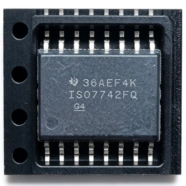
ISO7742FDBQR - 100Mbps 4-Ch Reinforced Digital Isolator | TI
The Texas Instruments ISO7742FDBQR is a high-speed, robust-EMC reinforced quad-channel digital isolator in a 16-pin SSOP (DBQ) package with 3.90mm body width. It provides four isolation channels in a 2-forward/2-reverse configuration, supporting data rates up to 100 Mbps and operation from supply voltages of 2.25V to 5.5V on each side, enabling seamless logic-level translation across the isolation barrier. A digital isolator is a component that transmits digital signals across a galvanic isolation barrier, protecting low-voltage circuitry and users from high voltages, ground loops, and common-mode noise. Within the interface-IC hierarchy, it sits between signal-chain ICs and hostile environments, complementing isolated power converters and isolated transceivers in industrial systems. The ISO7742FDBQR belongs to TI's ISO774x family, which uses an on-chip capacitive isolation structure with an oxide barrier, achieving reinforced isolation rated at 3000 Vrms. Key features include a common-mode transient immunity (CMTI) of 85 kV/us minimum, low power consumption, default-output (F suffix) fail-safe behavior that drives outputs low when the input side is unpowered, and a projected barrier lifetime exceeding 30 years at rated working voltage. The device is characterized from -55C to +125C, covering extended industrial and automotive-adjacent environments. Technically, the ISO7742FDBQR encodes input transitions across the capacitive barrier and decodes them on the secondary side, achieving sub-100 Mbps signaling with low propagation delay and low channel-to-channel skew without optocoupler aging effects. Its robust-EMC construction provides high immunity to surge and fast transient events typical of motor-drive and inverter environments. Typical applications include isolated SPI/UART interfaces, industrial fieldbus communication, motor drives and power inverters, and isolated ADC signal paths in renewable-energy systems. Pair it with devices such as the AMC1306M25 or ISO1042 for complete isolated measurement and communication chains. Design tip: maintain datasheet creepage and clearance on the PCB under the isolation barrier, avoid traces crossing the gap, and place 0.1uF decoupling capacitors close to both VCCI and VDD pins to preserve EMC performance.
ISO7830DW - 8000VPK Reinforced 3-Ch Digital Isolator | TI
The Texas Instruments ISO7830DW is a high-performance, triple-channel digital isolator with reinforced isolation rated at 8000-VPK (VIOWM 2000-VRMS) and 14.5-mm creepage. It comes in a 16-pin wide-body SOIC (DW) package and delivers robust galvanic isolation for industrial and automotive systems. The device supports data rates up to 100 Mbps in a 3/0 channel configuration (three forward channels, no reverse), ideal for unidirectional signal isolation. A digital isolator is a component that transfers digital signals across an isolation barrier while blocking DC and unwanted AC currents between two ground domains. Digital isolators sit within the broader hierarchy of interface ICs and optocoupler replacements, using capacitive coupling instead of LED-based optocoupling. They are essential in motor drives, power converters, and communication interfaces where galvanic isolation protects low-voltage control circuitry from high-voltage transients. Key features include a high common-mode transient immunity (CMTI) of 70-100 kV/us, low power consumption (approximately 1.5 mA per channel at 1 Mbps), and a wide supply range of 2.25 V to 5.5 V on both sides. The ISO7830 is certified by VDE, CSA, and TUV for reinforced isolation, and offers a fail-safe output (default low) when the input side is unpowered. Technically, the ISO7830 uses ON-OFF keying (OOK) modulation across an integrated high-voltage capacitive isolation barrier. This architecture provides immunity to magnetic interference, high-speed transmission, and low propagation delay (typically 10.7 ns). The device operates over the industrial temperature range of -40C to +125C and is offered in tube (DW) and tape-and-reel (DWR) options. Typical applications include isolated SPI, UART, and GPIO links in industrial automation, motor control, photovoltaic inverters, EV charging stations, and medical equipment. High CMTI and reinforced isolation ratings fit noise-heavy, high-voltage environments. Design tip: maintain datasheet creepage/clearance on the PCB, keep the area under the barrier free of traces, and decouple both VCC pins with 0.1 uF ceramics close to the pins. Pricing as of 2026-08-30; single-unit price is estimated from distributor quotes and marked for verification.
ISO7831DW - 100Mbps 3-Ch Reinforced Digital Isolator | TI
The Texas Instruments ISO7831DW is a high-performance, reinforced triple-channel digital isolator with a 2/1 channel configuration (two forward, one reverse) and signaling rates up to 100 Mbps. It comes in a 16-pin wide-body SOIC (DW) package providing 14.5 mm creepage and a VIOWM working voltage of 2000 Vrms, with 5700 VRMS isolation and 8000 VPK surge capability. A digital isolator is an integrated circuit that transmits digital signals across a galvanic isolation barrier, blocking high voltages, ground loops, and common-mode transients from reaching sensitive low-voltage circuitry. Within the interface IC hierarchy, digital isolators sit between logic-level translators and fully isolated transceivers; reinforced-class devices such as the ISO7831 represent the highest isolation category under IEC 60747-17. Key features include a common-mode transient immunity (CMTI) of 70 kV/us for reliable operation in noisy switching environments, dual 2.25 V to 5.5 V supplies compatible with low-voltage logic, and an enable pin for output tri-state control. Certifications include UL 1577, IEC 60747-17 (VDE), and CSA, supporting safety-critical end equipment. Technically, the ISO7831 uses TI's proprietary capacitive isolation technology, which outperforms optocouplers with lower power, higher speed, and longer lifetime. Propagation delay is approximately 11 ns with about 1 ns pulse-width distortion, preserving signal timing integrity across the barrier. Operating temperature spans -40C to +125C for harsh industrial conditions. Typical applications include motor-drive gate-control interfaces, isolated SPI/UART communication in industrial fieldbus systems, and power inverter control where reinforced isolation is mandated. High CMTI and low EMI also suit medical equipment requiring patient-safety isolation. Design tip: place 0.1 uF decoupling capacitors close to both VCC1 and VCC2 pins, and use the enable pin to force a defined output state during power sequencing.
ISOW6441 - 150Mbps Isolator w/ Integrated DC-DC | TI
The Texas Instruments ISOW6441 is a low-emissions, reinforced, quad-channel (3 forward / 1 reverse) digital isolator with an integrated high-efficiency DC-DC converter, delivering up to 150 Mbps data rate and up to 550 mW of isolated output power in a 16-pin wide SOIC (DW) package. It targets space-constrained isolated designs where a separate isolated power supply is impractical. A digital isolator provides galvanic isolation between two circuits while allowing digital signals to cross the isolation barrier via capacitive coupling, without a direct electrical connection. Within the isolation component hierarchy, the ISOW6441 belongs to the power-integrated digital isolator family - combining signal isolation with isolated power delivery, a subset of interface and signal isolation ICs. Key features include 150 Mbps data rate, 5000 Vrms isolation rating per UL 1577, 200 kV/us common-mode transient immunity (CMTI), and a selectable isolated output voltage of 3.3V or 5V with low 30 mV output ripple. The integrated DC-DC converter is emission-optimized to meet CISPR 32 Class-B on a 2-layer board, a best-in-class achievement per TI application note SBAA810. Technically, the ISOW6441 uses TI proprietary capacitive isolation technology for high-speed, low-power data transfer, and a push-pull converter topology with an integrated transformer for efficient, low-EMI power delivery. Default output is high on input signal loss (non-F variant); the F-suffix ISOW6441F defaults low. Operating temperature spans -40C to +125C. Typical applications include isolated SPI in industrial automation, isolated UART links, motor drive gate-driver supplies, and power-supply feedback isolation, where the integrated power eliminates a separate isolated DC-DC converter, reducing board space and BOM cost. Design tip: achieve specified CISPR 32 compliance by following the recommended datasheet PCB layout, maintaining adequate clearance/creepage for the reinforced isolation rating, and placing decoupling capacitors close to supply pins.

KSZ8001LI - 10/100 PHY Transceiver, MII/RMII/SMII | Microchip (Tape & Reel)
The Microchip Technology KSZ8001LI is a single-chip 10BASE-T/100BASE-TX/100BASE-FX physical layer transceiver that supports MII, RMII, and SMII host interfaces, housed in a 48-pin LQFP (7x7 mm) package with industrial -40C to +85C operating range. It integrates 3.3V single-supply operation, LinkMD cable diagnostics with up to 200m cable length measurement and ±2m accuracy, and robust 130m+ cable operation, making it a versatile Ethernet PHY for embedded designs. What is an Ethernet PHY transceiver? A Physical Layer device (PHY) is the analog front-end of an Ethernet link, sitting between the digital MAC controller and the magnetic transformer/RJ-45 connector. The PHY handles line coding (MLT-3 for 100BASE-TX, Manchester for 10BASE-T), clock/data recovery, adaptive equalization, and link-pulse detection. The KSZ8001LI belongs to the Fast Ethernet (100 Mbps) PHY family, which falls under Interface ICs -> Network Interface -> Ethernet Transceiver in the broader semiconductor hierarchy. Key differentiating features include LinkMD TDR-based cable diagnostics that detect open/short conditions and report cable length up to 200m with ±2m accuracy, robust operation over standard Cat-5 cables up to 130m+, HP Auto-MDIX support for automatic crossover detection, and flexible MII/RMII/SMII host bus selection that lets the same PHY connect to MACs with different pin-count constraints. The device supports both copper (100BASE-TX, 10BASE-T) and fiber (100BASE-FX) media via an external fiber transceiver. The KSZ8001LI architecture uses a 3.3V analog supply plus a 1.8V digital core derived from an internal LDO, with separate VDDIO rails supporting 3.3V or 2.5V MAC interface voltages. Typical power consumption is 172 mW. The PHY connects to a MAC via parallel MII (18 pins), reduced MII (RMII, ~9 pins), or serial MII (SMII, 4 pins), configured at reset via strap pins. Auto-negotiation follows IEEE 802.3u Clause 28. Typical applications include industrial Ethernet IP cameras, factory automation PLCs, networked printers, set-top box Ethernet ports, embedded IoT gateways with wired connectivity, and any embedded system requiring a small-footprint 10/100 Ethernet PHY with diagnostic capability. The LinkMD feature is particularly valuable in managed switches and remote installations where cable fault localization reduces service calls. Design considerations include providing a 25 MHz reference clock (or 50 MHz for RMII), placing the device within 25 mm of the magnetic transformer, implementing proper 50 ohm differential routing for the MDI traces, and supplying adequate decoupling (0.1 uF plus 10 uF bulk) on each supply rail. The KSZ8001LI differs from the -L variant (KSZ8001L) by offering higher-grade industrial temperature support and the -TR suffix denotes Tape and Reel packaging. This page synthesizes distributor pricing as of 2026-10-16, real drop-in alternatives sourced from cross-reference databases, and practical engineering considerations to accelerate Ethernet PHY selection beyond the bare manufacturer datasheet.
KSZ8001LI-TR - 10/100 PHY Transceiver, MII/RMII/SMII | Microchip
The Microchip Technology KSZ8001LI-TR is a single-chip 10BASE-T/100BASE-TX/100BASE-FX physical layer transceiver that supports MII, RMII, and SMII host interfaces, housed in a 48-pin LQFP (7x7 mm) package with industrial -40C to +85C operating range. It integrates 3.3V single-supply operation, LinkMD cable diagnostics with up to 200m cable length measurement and ±2m accuracy, and robust 130m+ cable operation, making it a versatile Ethernet PHY for embedded designs. What is an Ethernet PHY transceiver? A Physical Layer device (PHY) is the analog front-end of an Ethernet link, sitting between the digital MAC controller and the magnetic transformer/RJ-45 connector. The PHY handles line coding (MLT-3 for 100BASE-TX, Manchester for 10BASE-T), clock/data recovery, adaptive equalization, and link-pulse detection. The KSZ8001LI-TR belongs to the Fast Ethernet (100 Mbps) PHY family, which falls under Interface ICs -> Network Interface -> Ethernet Transceiver in the broader semiconductor hierarchy. Key differentiating features include LinkMD TDR-based cable diagnostics that detect open/short conditions and report cable length up to 200m with ±2m accuracy, robust operation over standard Cat-5 cables up to 130m+, HP Auto-MDIX support for automatic crossover detection, and flexible MII/RMII/SMII host bus selection that lets the same PHY connect to MACs with different pin-count constraints. The device supports both copper (100BASE-TX, 10BASE-T) and fiber (100BASE-FX) media via an external fiber transceiver. The KSZ8001LI-TR architecture uses a 3.3V analog supply plus a 1.8V digital core derived from an internal LDO, with separate VDDIO rails supporting 3.3V or 2.5V MAC interface voltages. Typical power consumption is 172 mW. The PHY connects to a MAC via parallel MII (18 pins), reduced MII (RMII, ~9 pins), or serial MII (SMII, 4 pins), configured at reset via strap pins. Auto-negotiation follows IEEE 802.3u Clause 28. Typical applications include industrial Ethernet IP cameras, factory automation PLCs, networked printers, set-top box Ethernet ports, embedded IoT gateways with wired connectivity, and any embedded system requiring a small-footprint 10/100 Ethernet PHY with diagnostic capability. The LinkMD feature is particularly valuable in managed switches and remote installations where cable fault localization reduces service calls. Design considerations include providing a 25 MHz reference clock (or 50 MHz for RMII), placing the device within 25 mm of the magnetic transformer, implementing proper 50 ohm differential routing for the MDI traces, and supplying adequate decoupling (0.1 uF plus 10 uF bulk) on each supply rail. The KSZ8001LI-TR differs from the -L variant (KSZ8001L) by offering higher-grade industrial temperature support and the -TR suffix denotes Tape and Reel packaging. This page synthesizes distributor pricing as of 2026-10-16, real drop-in alternatives sourced from cross-reference databases, and practical engineering considerations to accelerate Ethernet PHY selection beyond the bare manufacturer datasheet.
KSZ8041MLL - 10/100 Ethernet PHY | Microchip | MII
The Microchip Technology KSZ8041MLL is a single-port 10BASE-T/100BASE-TX Ethernet physical-layer transceiver with a full MII host interface, supplied in a 48-LQFP 7 x 7 mm package. It supports 10 Mb/s and 100 Mb/s Ethernet operation from a single 3.3 V supply. The device interfaces with an Ethernet media-access controller through MII, RMII, or SMII-compatible signaling and provides the physical-layer functions required to connect a digital controller to a 10/100 Ethernet network. An Ethernet PHY is a physical-layer transceiver within the broader Ethernet interface hierarchy. It converts digital frame data from a MAC controller into physical signals suitable for twisted-pair cabling and recovers those signals at the receiving endpoint. The KSZ8041 family combines a mixed-signal PHY implementation with configurable operating modes, reducing board area and power consumption while preserving compatibility with conventional Ethernet controller interfaces. Key features include support for 10BASE-T and 100BASE-TX links, full MII support on the MLL version, a single 3.3 V supply, and an integrated 48-pin LQFP package measuring 7 x 7 mm. The family also supports automatic crossover-related functions identified by Microchip as HP Auto MDI/MDIX. Configuration strapping pins establish speed, duplex, auto-negotiation, power-down behavior, and PHY-address settings when the device starts or resets. The mixed-signal architecture is central to the KSZ8041 implementation. Analog transmit and receive circuitry works with the digital MAC-facing interface, allowing the same PHY family to support copper links at 10 Mb/s or 100 Mb/s. MII provides a parallel data path between the PHY and controller, while the broader KSZ8041 family is documented with RMII and SMII interface support. Designers must still verify the exact interface and strap requirements of the selected ordering code against the manufacturer datasheet. Typical uses include embedded Ethernet ports, industrial controllers, communications equipment, network interface adapters, and systems using a Microchip-compatible 10/100 Ethernet controller. The KSZ8041MLL is especially relevant to designs that require the basic MII-supported PHY in a 48-LQFP surface-mount package rather than the TL or FTL ordering options described as TQFP packaged in the manufacturer data sheet. Layout is critical because the device combines high-speed digital interface signals with sensitive analog receive and transmit circuits. Follow the manufacturer's hardware design checklist, keep the PHY and magnetics interface area tightly controlled, provide the required decoupling, and avoid routing sensitive analog traces beneath digital or high-current paths. Verify magnetics, termination, reset, strap, and crystal or clock requirements before releasing the PCB. This page consolidates the verified distributor description, manufacturer data-sheet identification, package information, hardware-design guidance, and application-oriented engineering considerations. It also distinguishes the basic MII MLL variant from related KSZ8041 ordering codes and identifies where package, electrical, lifecycle, or compliance details require confirmation from the latest Microchip documentation.

KSZ8041NL-TR - 10/100 Ethernet PHY, MII/RMII, 32-QFN | Microchip
The Microchip KSZ8041NL-TR is a single-supply 10BASE-T/100BASE-TX physical layer (PHY) transceiver that provides MII and RMII MAC interfaces, housed in a 32-pin QFN (5x5 mm) package with HP Auto-MDIX support. The device operates from a single 3.3V supply (3.135V to 3.465V), supports 10/100 Mbps data rates per IEEE 802.3 and IEEE 802.3u, and integrates the line-side magnetics interface as well as baseline wander correction to extend signaling distance. A PHY (physical layer device) is the lowest tier of the Ethernet OSI stack, sitting just above the transformer/MDI and below the MAC layer. It handles line coding (MLT-3 / 4B5B), link training, auto-negotiation, and clock recovery. Within a typical embedded Ethernet design, a PHY sits between the magnetics plus RJ45 jack and an Ethernet MAC, either inside a microcontroller or as a separate controller; engineers select a discrete PHY when the host MCU/MAC lacks 10/100 support, when isolation or industrial temperature range is required, or when a broader MAC/PHY ecosystem has been validated for a given application. Key features of the KSZ8041NL-TR include 1/1 transceiver configuration with full MII and RMII MAC-side interfaces (SMII supported on the KSZ8041RNL version), HP Auto-MDIX crossover correction that eliminates the need for crossover cables, on-chip 1.8V regulator that can optionally power the MAC, low-power energy-detect mode, and linkMD cable diagnostics for opens, shorts, and cable length estimation. The mixed-signal design reportedly reduces power consumption versus competing 100 Mbps PHYs. Architecturally, the KSZ8041NL uses a DSP-based echo canceller and adaptive equalizer to achieve robust 100BASE-TX performance over CAT-5 cable, with HP Auto-MDIX implemented in the analog front end to autonegotiate polarity and pair roles. The MAC interface supports both MII (25 MHz reference clock at 100 Mbps) and RMII (50 MHz reference clock shared between MAC and PHY), enabling pin-compatible use with a wide range of microcontrollers. Typical applications include set-top boxes and IPTV gateways, network-capable printers and MFPs, industrial Ethernet sensors and PLCs, gaming consoles, and any embedded design that needs a 10/100 Ethernet port without a built-in PHY. The QFN-32 (5x5 mm) small footprint also suits space-constrained consumer and IoT appliances. When laying out this part, give the 50 MHz RMII clock trace a short, matched-length path to both the MAC and the PHY, and follow Microchip's KSZ8041NL Hardware Design Checklist for RJ45 magnetics pairing; do not skip the center-tap capacitor network on each line-side pair. This page compiles distributor pricing, drop-in alternatives, and PCB design notes not found in the bare datasheet, helping engineers select and place the KSZ8041NL-TR quickly.

KSZ9021GQI - Gigabit Ethernet PHY, GMII/MII, 128-PQFP | Microchip
The Microchip KSZ9021GQI is a triple-speed (10Base-T/100Base-TX/1000Base-T) Gigabit Ethernet physical-layer transceiver supporting GMII and MII MAC interfaces, housed in a 128-pin PQFP (14x20 mm) package. It delivers 1 Gbps data rate over standard CAT-5 unshielded twisted-pair cable with integrated termination and on-chip LDO regulators for analog and digital supplies, and operates from a single 3.3 V supply (3.135 V to 3.465 V). What is an Ethernet PHY transceiver? A PHY is the physical-layer device in the OSI stack that connects a link-layer MAC to the analog copper or optical medium, performing line coding, echo/return-loss cancellation, adaptive equalization, and clock/data recovery. The KSZ9021GQI is a single-port Gigabit PHY that combines the PCS (physical coding sublayer) and PMA (physical medium attachment) functions plus the analog front end, exposing a parallel GMII (Gigabit Media-Independent Interface) or MII to the host MAC. It sits below the MAC in the Ethernet stack and above the magnetics/RJ-45. Key features include 10/100/1000 Mbps operation on a single port, auto-negotiation and HP Auto-MDIX for crossover-polarity independence, four RGMII timing modes, per-port LED status drivers, JTAG and MDC/MDIO management, and a Wake-on-LAN link-change interrupt. Power consumption is about 400 mW active at 1000 Mbps and well below 100 mW in Energy-Efficient Ethernet (EEE) or software power-down modes. Typical industrial-grade operating temperature spans -40 C to +85 C. Internally, the silicon uses DSP-based adaptive equalization, a 125 MHz reference clock and a 1.25 GHz serializer, supporting both 1000Base-T PAM-5 (5-level pulse amplitude modulation across four twisted pairs simultaneously) and traditional 10/100BASE-TX MLT-3. A hardware-driven auto-MDI/MDIX eliminates the need for crossover cables and reduces system BOM. Typical applications include industrial Ethernet switches and routers, factory automation controllers, IP cameras and network video recorders, network-attached storage and embedded Linux networking, and telecommunications line cards. The 128-pin PQFP footprint is widely used on older and ruggedized designs that favor a leaded package over leadless QFN. When designing with this device, follow the typical-application circuit in the datasheet: four 1 percent 49.9 ohm termination resistors to the MDI pins, a 25 MHz reference crystal or external oscillator, 0.1 uF and 10 uF decoupling on each supply pin, and magnetics rated for 1000Base-T. Keep the analog/digital/PLL supply layouts separated by ferrite beads if specified. Note this part is moving toward end-of-life - confirm lifecycle status with Microchip before committing new designs.

KSZ9031RNXIA - Gigabit Ethernet PHY Transceiver RGMII | Microchip
The Microchip Technology KSZ9031RNXIA is a fully integrated triple-speed (10Base-T/100Base-TX/1000Base-T) Gigabit Ethernet physical-layer transceiver that supports 1.8V, 2.5V, and 3.3V I/O voltages with RGMII MAC interface, housed in a 48-pin QFN (7x7 mm) package with industrial temperature grade (-40C to +85C). The device provides a complete 10/100/1000 Mbps Ethernet PHY solution for transmission and reception over standard CAT-5 unshielded twisted pair (UTP) cable. An Ethernet PHY (Physical Layer transceiver) is a critical mixed-signal IC that sits between the digital MAC (Media Access Controller) in a processor/switch and the analog copper cable. PHY transceivers handle line coding (PAM-3/PAM-5 for 1000BASE-T), echo cancellation, crosstalk mitigation, and link training; they sit below the MAC in the OSI model hierarchy: PHY -> transceiver -> network interface -> wired connectivity IC. The KSZ9031 family occupies the Gigabit Ethernet PHY category within Power-over-Ethernet-aware wired networking semiconductors. Key features include Wake-on-LAN support, LinkMD cable diagnostics for cable plant fault detection, Auto-MDI/MDIX crossover, jumbo frame support up to 9.6 KB, and an integrated 1.2V LDO regulator. The RGMII interface supports 1.5V/1.8V/2.5V/3.3V HSTL, SSTL, or LVCMOS signaling to a wide range of MACs, FPGAs, and Ethernet switches. Energy-detect power-down and EEE (Energy Efficient Ethernet) further reduce system power consumption during idle link states. The KSZ9031 uses DSP-based echo and crosstalk mitigation, on-chip termination resistors, and adaptive equalization to deliver robust 1000BASE-T performance over marginal cable plants. The device provides two LED outputs, an MDIO management interface, and requires only a single 25 MHz reference clock. Typical applications include industrial Ethernet switches, factory automation controllers, automotive infotainment/networking, IP cameras and surveillance, network printers, and any embedded system requiring 10/100/1000 Mbps copper Ethernet connectivity with RGMII host interface. The KSZ9031 is AEC-Q100 qualified for automotive use. When designing with this device, provide a clean analog supply (AVDDH 3.3V) and digital supply decoupling per the datasheet reference circuit; place the 48-pin QFN thermal/exposed pad onto a proper ground-solder land with multiple thermal vias for reliable operation. Use the MDIO/MDC pins for PHY management and configuration. This page synthesizes distributor pricing, drop-in alternatives, and practical design notes not found in the manufacturer datasheet.

L9616-TR - LIN Bus Transceiver | STMicroelectronics | Automotive
The L9616-TR is a LIN (Local Interconnect Network) bus transceiver manufactured by STMicroelectronics, designed for automotive and industrial serial communication networks. It operates as a physical layer interface between the LIN protocol controller and the single-wire bus, supporting data rates up to 20 kbps as per the LIN standard. The device is available in an SO-8 package, making it suitable for space-constrained PCB designs. A LIN transceiver is a specialized integrated circuit that provides the physical layer for LIN networks, which are low-cost, single-wire serial communication buses used primarily in automotive body control applications. The transceiver converts the digital signals from the microcontroller's UART into bus-level voltages and vice versa, while providing protection against bus faults, ESD, and electromagnetic interference. In the system hierarchy, the LIN transceiver sits between the microcontroller (protocol layer) and the physical bus wire, forming the lowest layer of the LIN protocol stack. Key features of the L9616-TR include a wide operating voltage range of 5V to 27V, making it compatible with automotive battery voltages, and a low quiescent current for power-saving in standby modes. The device supports both normal and standby operating modes, with a wake-up capability via the bus line. It also features thermal shutdown and short-circuit protection, ensuring robust operation in harsh automotive environments. The SO-8 package provides a compact footprint with a thermal resistance of approximately 150 C/W, suitable for moderate power dissipation. The L9616-TR is built using STMicroelectronics' high-voltage BCD (Bipolar-CMOS-DMOS) technology, which integrates robust analog and digital circuitry on a single die. This technology enables the transceiver to handle high bus voltages and transient conditions while maintaining low power consumption. The device is fully compliant with the LIN 2.x and SAE J2602 standards, ensuring interoperability with other LIN nodes. Typical applications include automotive body control modules, door modules, seat control, steering column switches, and industrial sensor networks. The L9616-TR is also used in aftermarket automotive electronics and diagnostic tools. Its wide input voltage range and robust protection features make it ideal for direct connection to the vehicle battery. When designing with the L9616-TR, ensure proper bus termination (typically 1kΩ to 10kΩ pull-up to battery) and place a 100nF bypass capacitor close to the VCC pin. The TXD and RXD pins interface directly with the microcontroller's UART, and the INH pin can be used to control an external voltage regulator for power management in sleep mode.
L9969-TR - Automotive LIN Transceiver | STMicroelectronics
The L9969-TR is an automotive-grade LIN (Local Interconnect Network) transceiver from STMicroelectronics, designed for in-vehicle networking applications. It operates as a single-wire transceiver compliant with LIN 2.x and SAE J2602 standards, providing a robust physical layer interface between the LIN protocol controller and the single-wire bus. The device is available in a compact 8-pin SOIC (SO-8) package, making it suitable for space-constrained automotive electronic control units (ECUs). A LIN transceiver is a physical layer device that connects a microcontroller's UART to a single-wire bus, enabling communication at data rates up to 20 kbps. It converts the microcontroller's logic-level signals to the bus voltage levels (typically 12V) and provides protection against short circuits, overvoltage, and ESD. In the automotive network hierarchy, the LIN transceiver sits between the LIN protocol controller (often integrated in the MCU) and the physical bus, forming the lowest-cost networking layer below CAN and FlexRay. It is essential for body control modules, smart actuators, and sensor nodes. Key features of the L9969-TR include a wide operating voltage range of 5.5V to 18V (with 40V load dump protection), a low quiescent current of 10 uA in sleep mode, and a data rate of up to 20 kbps. It supports both 3.3V and 5V microcontroller interfaces, and includes a dominant state timeout and thermal shutdown protection. The device is AEC-Q100 qualified, ensuring reliability in harsh automotive environments. The L9969-TR uses a robust BiCMOS process technology, integrating a high-voltage bus driver, a receiver with slew-rate control, and protection circuitry. Its architecture ensures low electromagnetic emission (EME) and high electromagnetic immunity (EMI), meeting stringent automotive EMC requirements. The device also features a dedicated INH (inhibit) pin for controlling an external voltage regulator, enabling efficient power management in sleep mode. Typical applications include body control modules, door modules, seat control, steering column switches, and smart actuators. The L9969-TR is also used in LIN-based sensor nodes for climate control and lighting systems. Its low quiescent current makes it ideal for battery-powered modules that must remain in sleep mode for extended periods. When designing with the L9969-TR, ensure proper bus termination (typically 1 kOhm to 5V) and place a 220 pF capacitor on the bus line for EMC filtering. The INH pin should be connected to the enable input of the voltage regulator to achieve low standby power consumption. For thermal management, the SO-8 package has a thermal resistance of 150 C/W, so adequate PCB copper area is recommended for high-temperature environments.
LAN8741A-EN - 10/100 Ethernet Transceiver | Microchip
The Microchip Technology LAN8741A-EN is a small-footprint 10/100 Mb/s Ethernet physical-layer transceiver with MII and RMII interfaces, Energy Efficient Ethernet support, HP Auto-MDIX, and flexPWR technology in a 32-SQFN 5 x 5 mm package. It operates from a 1.62 V to 3.6 V core supply, automatically negotiates speed and duplex mode, and accepts straight-through or crossover LAN cables through HP Auto-MDIX. An Ethernet physical-layer transceiver, commonly called an Ethernet PHY, converts between digital MAC-layer data and analog signals carried by twisted-pair Ethernet. It sits within the Ethernet interface hierarchy as a physical-layer IC, below the Ethernet MAC controller and above the transformer-coupled network cable. The LAN8741A-EN supports both MII and RMII host interfaces, allowing it to serve designs using either a parallel Media Independent Interface or the reduced-pin Reduced MII interface. Key features include 10/100 Mb/s operation, Energy Efficient Ethernet, HP Auto-MDIX, flexPWR low-power technology, and deterministic loopback delay for repeatable real-time system behavior. IEEE 802.3-2005 compliance is explicitly stated for supported functions, while additional vendor-specific register functions are also available. The 32-SQFN package reduces board area compared with larger Ethernet PHY implementations, although proper high-speed layout and magnetics isolation remain essential. The LAN8741A-EN integrates the physical-layer functions needed to establish a 10 Mb/s or 100 Mb/s copper Ethernet link. Automatic negotiation selects the highest common speed and duplex mode available on the connected network. HP Auto-MDIX removes the need for a straight-through versus crossover cable decision, while Energy Efficient Ethernet and flexPWR address system power requirements when traffic is idle or the network is lightly loaded. Typical uses include embedded industrial Ethernet equipment, factory automation controllers, building-automation gateways, networked sensors, set-top boxes, printers, IP cameras, and compact communication modules. Its MII compatibility supports legacy parallel-interface architectures, while RMII is appropriate for modern reduced-pin connections to an Ethernet MAC or microcontroller. PCB design should prioritize short, controlled-impedance traces for RMII and MII signals, a clean split between digital and analog circuitry, solid ground-plane continuity, and correct component placement around the PHY and 10/100 Ethernet transformer. The manufacturer's application guidance and datasheet should be followed for magnetic-component selection, termination, decoupling, and layer-stack recommendations. This product page consolidates verified manufacturer and distributor information, practical PCB guidance, package details, and same-family drop-in alternatives into one engineering reference. It also distinguishes confirmed substitute options from products that are merely functionally similar but require a different footprint or interface arrangement.
LAN8770M-I/PRA - 100BASE-T1 Automotive Ethernet PHY | Microchip
The Microchip Technology LAN8770M-I/PRA is a single-port 100BASE-T1 Ethernet physical layer (PHY) transceiver delivering 100 Mbit/s transmit and receive capability over a single Unshielded Twisted Pair (UTP) cable, compliant with the IEEE 802.3bw-2015 standard, housed in a 32-pin VQFN (5x5 mm) package with exposed pad and wettable flanks. An Ethernet PHY transceiver is the physical-layer device in the OSI model that converts digital MAC-layer frames into analog signals suitable for transmission over copper media. Within the network hierarchy - Ethernet MAC, PHY transceiver, magnetics/connectors, cable - the PHY sits directly between the MAC and the physical medium, handling encoding, equalization, echo cancellation, and link management. In the 100BASE-T1 (formerly automotive BroadR-Reach) category, the PHY enables full-duplex 100 Mbit/s communication over a single unshielded twisted pair, dramatically reducing cabling weight and cost compared with 100BASE-TX. Key features of the LAN8770M include MAC interface support for standard MII and RMII protocols, an integrated SMI (Serial Management Interface) for rapid register access and configuration, and an optional 50 MHz reference clock output for RMII applications. The M-variant adds Reverse MII mode, which allows two PHYs to be connected back-to-back - useful in media converter and test architectures. Unlike the LAN8770R variant, this device does not include an RGMII interface, keeping cost and pin count low. Technically, the device integrates the analog front end, ADC/DAC signal path, and DSP equalization required for single-pair operation on one 1.1 V core supply with 3.3 V I/O, supporting -40C to +85C operation for demanding vehicular and industrial environments. Typical applications include automotive ECU-to-ECU networking, ADAS camera and sensor links, 100BASE-TX to 100BASE-T1 media conversion (as demonstrated on Microchip's EVB-LAN8770M_MC evaluation board), and industrial single-pair Ethernet backbones. Design consideration: 100BASE-T1 requires a single differential pair with common-mode termination and isolation network per the reference design; follow Microchip's layout guidance for the exposed pad thermal/electrical ground connection. This page synthesizes distributor pricing, drop-in family alternatives, and practical design notes not found in the manufacturer datasheet alone.
LAN8770M-I/PRA - 100BASE-T1 Ethernet PHY, VQFN-32 | Microchip
The Microchip LAN8770M-I/PRA is a single-port 100BASE-T1 Ethernet physical layer (PHY) transceiver delivering 100 Mbit/s transmit and receive capability over a single Unshielded Twisted Pair (UTP) cable, compliant with the IEEE 802.3bw-2015 automotive Ethernet specification, housed in a 32-pin VQFN (5x5 mm) package with exposed pad and wettable flanks. An Ethernet PHY transceiver is the physical-layer device in the network hierarchy that converts digital MAC frames into analog signals suitable for transmission over copper media. Positioned between the Ethernet MAC (typically inside an MCU, MPU, or switch) and the physical cable, the PHY handles encoding, line drivers, equalization, and clock recovery. The 100BASE-T1 standard (formerly BroadR-Reach) enables single-pair cabling at 100 Mbit/s, reducing weight and cost versus conventional two-pair 100BASE-TX. Key features of the LAN8770M include support for standard MII and RMII MAC interfaces, an optional 50 MHz reference clock output for RMII applications, and the distinctive Reverse MII mode that allows two PHYs to be connected back-to-back for media converter and bridge applications. An integrated SMI (Serial Management Interface) provides rapid register access and configuration. Technically, the device integrates the analog line drivers, adaptive equalizers, and echo cancellation needed for single-pair operation, while the digital core handles 4B/5B encoding and interface multiplexing. The 'M' variant is specifically the Reverse MII member of the LAN8770 family; the LAN8770R adds RGMII support with an optional 125 MHz clock output. Typical applications include automotive in-vehicle networking (camera links, ECUs, gateways), industrial media converters such as Microchip's EVB-LAN8770M_MC 100BASE-TX to 100BASE-T1 converter reference, factory automation sensor nodes, and compact IoT edge devices where single-pair cabling saves harness cost. Design consideration: the 32-VQFN exposed pad must be soldered to a solid ground plane for thermal and EMI performance, and the RMII reference clock routing requires length-matched traces. Verify the exact supply rails, current consumption, and MAC interface voltage levels in the manufacturer datasheet before finalizing power tree design. This page synthesizes distributor pricing, family-level drop-in alternatives, and practical design notes not found in the manufacturer datasheet, with all data verified as of 2026-10-19.

LAN8770RT-I - 100BASE-T1 Single-Pair Ethernet PHY | Microchip
The Microchip Technology LAN8770RT-I (orderable LAN8770RT-I/5KX) is a compact, cost-effective single-port 100BASE-T1 Ethernet physical layer (PHY) transceiver delivering 100 Mbit/s transmit and receive capability over a single Unshielded Twisted Pair (UTP) cable, housed in a 36-pin VQFN (6x6 mm) exposed-pad package with wettable flanks. A single-pair Ethernet (SPE) PHY is a physical-layer device that converts the digital MAC-layer signals of a media access controller into analog signals suitable for transmission over twisted-pair cabling. Within the network hierarchy - MAC, PHY, transformer, connector - the PHY occupies the layer that determines compliance with physical-layer standards. The LAN8770 complies with the IEEE 802.3bw-2015 (100BASE-T1) automotive Ethernet specification, supporting cable lengths of up to at least 15 meters over a single unshielded twisted pair. Key features include full MII and RMII media-independent interfaces for connection to a wide range of MACs and microcontrollers, a 1.1 V core supply domain, 4/4 driver/receiver configuration, and industrial temperature operation from -40C to +85C. The wettable-flank QFN package supports reliable solder-joint inspection in automotive-grade assembly processes, and the exposed pad provides low-impedance thermal and ground paths. Technically, the LAN8770 integrates the analog front end, ADC/DSP-based equalization, echo cancellation, and clock recovery required for robust single-pair signaling per IEEE 802.3bw-2015. Because 100BASE-T1 uses full-duplex transmission on one pair rather than two pairs as in 100BASE-TX, hybrid echo cancellation is a critical block, and Microchip's DSP architecture addresses this while keeping the bill of materials compact. Typical applications include automotive camera and sensor links, ECU-to-ECU in-vehicle networking, industrial PROFINET-style single-pair field links, and compact IoT gateways where four-wire cabling is unnecessary. The RMII interface makes it a natural companion to NXP, STMicroelectronics, and Microchip MCUs. When designing, pay close attention to the 1.1 V core supply sequencing and the magnetics-free single-pair link termination, which differs from conventional 100BASE-TX designs. The exposed pad must be soldered to a solid ground pour for thermal and EMI performance. This page synthesizes verified distributor data, compliance details, pricing availability guidance, and design notes not found in the manufacturer datasheet, providing engineers with a single citable reference.

LTC4302-1 - Addressable 2-Wire Bus Buffer | Analog Devices
The Linear Technology (Analog Devices) LTC4302-1 is an addressable 2-wire bus buffer with high noise margin, operating from a 2.7V to 5.5V supply in an 8-pin SO-8 (or MSOP-8) surface-mount package. It provides I2C Fast Mode (400 kHz) compatible buffering with 50 ns minimum glitch filtering on the SDAIN and SCLIN signals, and offers 32 selectable addresses via an external resistive divider on the ADDRESS pin. A 2-wire bus buffer is an integrated circuit that isolates and regenerates I2C or SMBus signals between a controller segment and a peripheral segment of the same bus. In the power-management hierarchy of system electronics, bus buffers sit between the host controller and the distributed peripherals, functioning as signal repeaters that allow capacitive load splitting, live-board insertion, and improved noise immunity. The LTC4302-1 belongs to the broader family of I2C buffers, SMBus buffers, and bus repeaters within mixed-signal interface ICs. Key differentiating features include hot-swap capability that permits a peripheral board to be inserted into or removed from a live backplane without corrupting the bus, rail-to-rail input glitch filtering of up to 50 ns duration pulses, and the ADDRESS pin architecture that provides 32 possible addresses set by an external resistive divider between VCC and GND. When VCC is low, the SDA and SCL inputs and outputs do not load the bus lines, a critical behavior for multi-card backplane systems. Technically, the LTC4302-1 uses rise-time accelerator circuitry and high noise margin level shifting on both the SDA and SCL channels. Per the Analog Devices datasheet (4302fs), the glitch filters prevent signals of up to 50 ns minimum duration and rail-to-rail voltage magnitude from passing into the 2-wire bus digital interface circuitry, ensuring robustness against backplane transients at Fast Mode 400 kHz operation. Typical applications include live-backplane peripheral card insertion in telecom and datacenter equipment, SMBus-aware server power-supply management, and I2C bus extension where bus capacitance exceeds the 400 pF standard limit. The LTC4302-1 variant's specific offset/slope behavior suits designs where an exact DC offset on the buffered segment is required. Design consideration: the ADDRESS pin resistive divider must use 1% or better tolerance resistors, and supply voltage must remain within 2.7V to 5.5V to guarantee glitch-filter timing and drive specifications. This page synthesizes distributor data, drop-in same-family alternatives, and practical design notes not found in the manufacturer datasheet alone.

LTC4307IMS8#TRPBF - Hot Swappable 2-Wire Bus Buffer | Analog Devices
The Analog Devices LTC4307IMS8#TRPBF is a low offset hot swappable 2-wire bus buffer with stuck bus recovery, supporting 400kHz I2C/SMBus operation in an 8-lead MSOP package (3.00mm width). It allows I/O card insertion into a live backplane without corrupting the data and clock busses. A 2-wire bus buffer, sometimes called an I2C buffer or bus repeater, is an interface IC that isolates the capacitance and voltage levels of two segments of an I2C or SMBus. In the system hierarchy it sits between the physical bus wires and the master or slave devices, forming part of the broader interface and signal-buffer family. Its role is to let one segment carry heavy loads (many devices, long cables, large capacitance) while the other segment presents only the buffer's very low input capacitance. Key features of the LTC4307 include bidirectional buffering that keeps backplane and card capacitances isolated, sub-10pF data and clock input capacitance on the card side, a low offset voltage architecture that accurately passes logic levels, and stuck bus recovery logic that frees a bus segment when a slave device holds SDA low. The hot swap capability means connections can be made and broken with the backplane powered, a critical property for ATCA, blades, and server storage platforms. Technically, the LTC4307 uses Analog Devices' rising-edge accelerators and digital rise-time recognition to distinguish valid start and stop conditions from slow edges caused by heavy bus capacitance. This allows 400kHz operation even when the buffered segment is heavily loaded, while level-shifting and offset compensation preserve timing margins across both bus segments. Typical applications include live-backplane I/O card insertion, HDMI DDC bus isolation, server and storage management SMBus isolation, and telecom line-card 2-wire bus segmentation. In each case the buffer prevents bus lockups during insertion events and extends the usable bus capacitance beyond the 400pF limit of a raw I2C segment. Design consideration: connect the ENABLE pin correctly for power sequencing and provide a small bypass capacitor on each VCC pin; during hot insertion the buffer must be the first element to see the backplane bus so card capacitance never appears on the backplane segment. This page synthesizes distributor pricing, drop-in alternatives (including the Renesas ISL33001IUZ cross-brand equivalent), and practical design notes not found in the manufacturer datasheet.
MAX13487EESA+T - 5V RS-485/RS-422 Transceiver | Maxim Integrated
The Analog Devices (Maxim Integrated) MAX13487EESA+T is a +5V half-duplex RS-485/RS-422-compatible transceiver with ±15kV ESD protection, proprietary AutoDirection control, and 500 kbps data rate, housed in an 8-pin NSOIC (SOIC-8, 3.90mm width) package with one driver and one receiver. An RS-485/RS-422 transceiver is a differential interface IC that converts single-ended logic signals into differential bus signals, sitting within the interface IC hierarchy of serial communications semiconductors. Half-duplex RS-485 transceivers share one differential pair for both transmit and receive, so direction control is a key architectural decision. Traditional parts require a microcontroller GPIO to drive the DE/RE pins; the MAX13487E instead uses Maxim's AutoDirection architecture, which senses the driver input and enables the driver automatically. Key features include true fail-safe receiver circuitry guaranteeing a logic-high receiver output when inputs are shorted, open, or idle, hot-swap capability that eliminates false transitions on the bus during power-up or live insertion, and ±15kV ESD protection on the transceiver pins. The /SHDN pin reduces supply current for low-power systems, and /DI, /RE and /SHDN pins are rated from -0.3V to +6V, allowing direct interfacing with 3.3V microcontrollers without level shifting. Architecturally, the device integrates one driver and one receiver operating from a +5V supply, with receiver input being 1/8 unit load, permitting up to 256 transceivers on a shared bus (per Cosine reference to equivalent-class devices). AutoDirection removes firmware overhead and timing errors associated with GPIO direction switching in polled half-duplex protocols. Typical applications include industrial fieldbus and Profiling nodes, building automation and HVAC controllers, motor/drive networks, battery-management stacks, and embedded metering where robust differential communication over long cables is required. Design consideration: the hot-swap feature matters when nodes are inserted into a live backplane; for software-controlled designs a conventional DE/RE part may be preferred instead. Verify bus biasing resistors for idle-state fail-safe operation. This page synthesizes distributor availability data, cross-reference findings, and practical design notes not found in the manufacturer datasheet alone.