Arayüz IC'leri
Alt Kategoriler
Ürünler (2.300+)
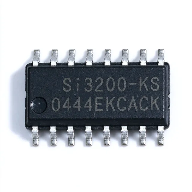
SI3200-KS - Dual Programmable CMOS SLIC | Skyworks
Skyworks Solutions Inc. SI3200-KS is a dual-channel Subscriber Line Interface Concept (SLIC) integrated circuit for customer-premise telephone equipment, combining a programmable CMOS line interface with line monitoring in a 16-pin SOIC package. Its key characteristics are dual-channel integration, standby power below 65 mW per channel, internal balanced ringing up to 65 Vrms, and software-programmable operating parameters. The SI3200-KS is intended for compact analog telephone and voice-over-data equipment that requires integrated line driving and supervision functions. A Subscriber Line Interface Concept, or SLIC, is an integrated line-interface circuit used in customer-premise equipment. It forms the analog signaling path between a telephone line and the equipment codec or voice-processing electronics. In the product hierarchy, a SLIC is a specialized telecom interface IC: it sits above general-purpose transceivers and codecs while providing the line-specific voltage, current, ringing, and supervision functions required by analog telephone networks. The SI3200-KS provides two SLIC channels in one package, reducing board area compared with separate single-channel implementations. Its software-programmable parameters allow an equipment designer to configure ringing frequency, line impedance behavior, and other interface characteristics through the control system. Internal balanced ringing to 65 Vrms supports telephone-line signaling without requiring a separate balanced-ringing circuit for every channel. The device emphasizes low standby power, with the manufacturer data describing consumption below 65 mW per channel. This characteristic is relevant in customer-premise equipment that may remain connected to a telephone line while the user is not actively making a call. Consolidation into one dual-channel IC can also reduce package count, although actual board savings still depend on the surrounding protection, isolation, codec, and magnetics arrangement. Typical uses include analog telephone adapters, voice gateways, customer-premise line cards, and other dual-channel voice terminals. A complete voice terminal still requires supporting components such as a speech codec, line protection, isolation components, and the appropriate external line circuitry. The SI3200-KS therefore occupies the line-interface portion of the design rather than replacing the codec or the entire telephone front end. When designing around the SI3200-KS, verify the complete external line interface against the manufacturer’s recommended schematic and component values. Pay particular attention to line-voltage and ringing limits, external protection, grounding, and the relationship between programmed line parameters and the codec interface. The verified source material does not provide a complete pin list, so board-level pin assignment must be checked against the manufacturer documentation rather than inferred from the distributor description. This product page consolidates verified distributor information, a source-backed technical description, practical application guidance, and a structured comparison of the available same-family references. It distinguishes confirmed facts from parameters that still require direct verification from the full manufacturer datasheet, helping engineers evaluate the obsolete SI3200-KS without relying on ambiguous cross-reference listings alone.

SI3201-BS - Programmable CMOS SLIC with Ringing | Skyworks
Skyworks Solutions Inc. SI3201-BS is a programmable CMOS subscriber line interface circuit (SLIC) with integrated codec, ringing-voltage generation, and battery-voltage generation in a 16-pin SOIC package. It supports supply voltages of 3.13 V to 5.25 V, software-programmable internal balanced ringing up to 90 VPK, and PCM, serial, or SPI interface options. The device is designed for short-loop customer premises equipment and telephone-interface applications. A subscriber line interface circuit is a mixed-signal telecommunications integrated circuit that connects a central-office or VoIP analog line to a digital voice system. In the component hierarchy, a SLIC is an interface IC, a telecommunications semiconductor, and a system-on-chip integration of line-driving, codec, ringing, and battery functions. This integration reduces the number of external components required in customer premises equipment while placing analog line control under software management. The SI3201-BS combines a low-voltage CMOS implementation with a software-programmable SLIC and codec interface. Its internal balanced ringing generator supports 90 VPK output. The stated ringing capability includes five REN at 4 kft and three REN at 8 kft, allowing the ringing load to be evaluated for different loop lengths. The integrated battery supply provides dynamic voltage output for the line interface. The device accepts a 3.13 V to 5.25 V supply range and can operate with PCM, serial, or SPI control interfaces. Reported operating supply current is 1 mA for the series, while another distributor result lists 88 mA for the SI3201-BS; these figures should be checked against the exact test conditions in the manufacturer datasheet before they are used in a power budget. Maximum power dissipation is reported as 800 mW, making thermal design and copper area relevant in space-constrained designs. Typical uses include analog terminal adapters, cable telephony equipment, wireless local-loop systems, and other CPE products requiring one-channel analog telephone interfaces. The SI3201-BS is particularly relevant when a short-loop design needs integrated linefeed control, codec communication, ringing generation, and programmable battery voltage in one IC. Before finalizing a PCB design, verify the complete 16-pin pinout, exposed-pad status, absolute maximum ratings, ringing waveform limits, and external network requirements against the manufacturer datasheet. The available search evidence confirms the 16-SOIC configuration and principal SLIC functions, but it does not provide a reliable pin-by-pin assignment table or complete electrical characteristic set. This page consolidates verified distributor information, package details, interface capabilities, application guidance, and source links into an engineering-focused reference. It also clearly distinguishes documented characteristics from parameters that still require confirmation from the manufacturer datasheet, avoiding unsupported component substitutions.
SI3201-FS 100V Linefeed Interface IC | Skyworks | 16-SOIC
The Skyworks Solutions, Inc. SI3201-FS is a Subscriber Line Interface Concept (SLIC) integrated circuit designed for customer premise equipment and analog telephone interface applications. It is identified as a 100 V linefeed interface IC for the Si321x family, with a codec interface, programmable CMOS SLIC architecture, integrated battery supply, and software-programmable ringing voltage generation. The device is supplied in a 16-pin SOIC package and is marketed as a lead-free component. The SI3201-FS addresses the subscriber-line side of a voice terminal or CPE design by combining linefeed control, ringing-voltage generation, battery feed, and codec interfacing in one IC. Its programmable architecture allows the system to configure line parameters and ringing behavior through software rather than relying on a large collection of discrete telephone-network components. The listed electrical headline is a 100 V linefeed interface, while the device description identifies programmable internal balanced ringing up to 90 VPK under specified REN and loop-length conditions. A key feature is the integrated battery supply with dynamic voltage output. In a telephone design, this function supports the line DC feed required by the subscriber line while allowing the system to manage line conditions dynamically. The software-programmable codec interface simplifies connection between the line interface and a digital voice processor or system controller. Because the SI3201-FS is intended for a 16-SOIC footprint, it can be integrated into CPE hardware with a surface-mount assembly process rather than through-hole insertion. Typical applications include analog telephone adapters, voice over IP terminals, residential gateways, digital subscriber line equipment, and other CPE products requiring a programmable analog line interface. The device should be selected only when the host design supports the associated ProSLIC software, codec interface, ringing and battery requirements, and the specified line parameters. The SI3201-FS is not a general-purpose low-voltage regulator or a replacement for a conventional codec. For implementation, engineers must follow the manufacturer datasheet for hook-state behavior, linefeed current, ringing limits, battery voltage, external component selection, and software configuration. Particular attention should be paid to the 100 V linefeed classification and the 90 VPK balanced ringing capability, since these values determine insulation, creepage, transient protection, and PCB spacing requirements. This page consolidates the verified distributor descriptions, package information, sourcing links, and application guidance for engineers evaluating the SI3201-FS.
SI3201-GS - Programmable CMOS SLIC with 90 V Ringing | Silicon Laboratories
The Silicon Laboratories SI3201-GS is a programmable CMOS subscriber line interface circuit that integrates SLIC, codec, ringing-voltage generation, and battery-supply functions in a 16-pin SOIC exposed-pad package. It operates from a 3.3 V or 5 V system supply, accepts a 3.3 V to 35 V DC input for battery generation, and provides balanced ringing up to 90 VPK. The device supports 5 REN at 4 kft and 3 REN at 8 kft line loading conditions. Its integrated approach reduces the number of external telephone-interface components required in voice-over-packet, analog terminal, and central-office line-card designs. Programmable interface characteristics make it suitable for telephone equipment requiring configurable line supervision, codec interfacing, and on-hook power generation. A subscriber line interface circuit, commonly called a SLIC, is the analog front end used between a telephone line and a digital voice processor. In the broader hierarchy, a SLIC is a telephone interface IC, while the SI3201-GS additionally combines codec interfacing and battery or ringing generation in one programmable CMOS device. This integration can simplify board partitioning, but the system must still provide appropriate protection, isolation, line filtering, and hook-state interfaces around the chip. Key features include software-programmable SLIC and codec behavior, internal balanced ringing rated to 90 VPK, an integrated battery supply with dynamic voltage output, and an on-chip DC-DC converter. The verified distributor data identifies a one-channel implementation with 60 dB channel isolation, approximately 41 mA operating current, a 3.13 V to 5.25 V supply range, and operation from -40°C to 85°C. The SI3201-GS also appears as a lead-free, 100 V linefeed interface option for use with Si321x-family companion devices. Technically, the device combines a low-voltage CMOS signal path with high-voltage line functions. Its DC-DC converter provides tracking battery from a 3.3 V to 35 V input, allowing the caller-side supply to track line voltage while the core interface operates from a 3.3 V or 5 V rail. This separation between logic supply and line-feed input improves design flexibility, but it also requires careful validation of converter layout, protection paths, and thermal performance. Typical applications include analog telephone adapters, voice-over-IP terminals, small PBX line cards, digital loopback or line-interface test equipment, and embedded voice systems that need programmable ringing and hook detection. In these systems, the SI3201-GS handles the physical line side while a DSP or system controller configures operating parameters through its digital interface. Design consideration: the exposed pad must be connected to the recommended ground plane, and high-voltage ringing paths require validated creepage, clearance, protection components, and isolation boundaries. Telephone interfaces are safety-critical, so final circuit compliance depends on the complete product design rather than the IC alone. This page consolidates verified distributor specifications, same-family drop-in candidates, comparison fields, and practical implementation guidance that are not presented together on a typical distributor listing.
SI3201-KS - Programmable CMOS SLIC with Ringing | Silicon Labs
The Silicon Labs SI3201-KS is a low-voltage programmable CMOS subscriber line interface circuit and codec for customer premises equipment, with software-programmable ringing and battery-voltage generation. It supports internally balanced ringing up to 90 VPK, including 5 REN at 4 kft and 3 REN at 8 kft, and is supplied in a 16-SOIC package with an exposed pad. The SI3201-KS combines the linefeed interface, codec interface, ringing generator, and battery supply in one CMOS IC. A SLIC, or subscriber line interface circuit, is an analog telephone-interface component that connects a central-office telephone line to customer equipment. It belongs to the telephone-interface IC hierarchy, where it bridges a high-voltage analog line and low-voltage digital or analog circuitry. The SI3201-KS is specifically associated with ProSLIC-type customer premises equipment and provides a programmable alternative to discrete linefeed networks. Principal features include software programmability, a codec interface, internal balanced ringing generation up to 90 VPK, and an integrated battery supply with dynamic voltage output. Distributor listings describe the device as a 100 V linefeed interface for Si321x applications. The 16-SOIC package measures 0.154 inch, or 3.90 mm, in width and uses an exposed-pad thermal and construction option. The device combines high-voltage analog line-interface functions with low-voltage CMOS control logic. Its programmable architecture allows ringing and line parameters to be configured through the associated control system rather than relying only on fixed passive networks. The exact supply voltages, DC feed characteristics, codec interfaces, temperature range, and absolute maximum ratings are not fully exposed in the supplied search records and should therefore be confirmed in the manufacturer datasheet. Typical applications include analog telephones, voice-over-IP terminals, DSL or broadband customer premises equipment, analog fax machines, voice gateways, and other carrier-facing or analog telephone adapters. The SI3201-KS is most appropriate where an integrated, programmable SLIC can simplify the line-interface section and reduce discrete external circuitry. The principal design consideration is the high-voltage line and ringing interface. PCB creepage, isolation, component spacing, surge protection, and thermal performance require careful attention even though the IC itself is a low-voltage CMOS device. Designers should also confirm the exposed-pad land pattern, required external components, and codec compatibility against the exact manufacturer datasheet before layout release.

SI3210-BT - Programmable SLIC/CODEC with Ringing | Skyworks
The Skyworks Solutions, Inc. SI3210-BT is a programmable CMOS subscriber line interface circuit and codec (SLIC/CODEC) with integrated ringing and battery-voltage generation. It supports one telephone line, 3.3 V or 5 V operation, and the SI3210 family is offered in a 38-pin TSSOP configuration. The device consolidates line-interface, voice-processing, DTMF, and telephone-signaling functions into one integrated circuit. A SLIC is an interface IC that connects a digital communications system to an analog telephone line. Typical SLIC functions include DC feed, line termination, ring voltage generation, line supervision, codec conversion, tone generation, and caller-ID signal handling. By placing these functions in a programmable CMOS device, the SI3210-BT allows system designers to adapt line behavior through manufacturer-defined control registers rather than using a large collection of discrete telephone components. The SI3210/Si3211 family supports software-configurable ringing with up to five REN and 90 VPK, along with DTMF generation and decoding and Caller ID generation. These capabilities make the family applicable to analog telephone adapters, voice-over-IP terminal equipment, digital subscriber line terminal designs, customer-premises equipment, and other line-powered telecom products. The family documentation also describes comprehensive telephony signaling support for global operation. The SI3210-BT is identified in comparison data as a one-channel SLIC with 60 dB performance and approximately 41 mA operation from 3.3 V or 5 V supplies. The -BT suffix denotes the 38-pin TSSOP ordering option. Because the SI3210-BT is marked obsolete, engineers should confirm availability, lifecycle expectations, and the exact package drawing before beginning a new production design. A robust line-interface design must account for high ringing voltage, transient protection, hook-state transitions, analog isolation, and PCB creepage. The ring generator can reach 90 VPK, so external protection and insulation coordination are essential even though the ringing function is integrated. Firmware configuration and production test should also be treated as part of the product design rather than treating the IC as a fixed-function codec. This page consolidates verified family specifications, sourcing links, package constraints, and practical line-interface guidance. It also distinguishes the documented SI3210 options from unverified assumptions, helping engineers evaluate obsolete inventory without presenting it as a currently recommended new-design choice.

SI3215-C-FM - ProSLIC SLIC/Codec with 90VPK Ringing | Skyworks
The Skyworks SI3215-C-FM is a single-channel ProSLIC Subscriber Line Interface Concept (SLIC) and CODEC IC housed in a 38-pin QFN (5x7 mm) package, integrating software-configurable 5 REN internal ringing up to 90 VPK, DTMF generation, and a comprehensive set of telephony signaling capabilities with expanded support for Japan and China country requirements. It pairs with the Si3201 line-side DC-DC controller (in a thermally-enhanced 16-pin SOIC) to form a complete FXS interface solution. Supply voltage is 3.13V to 5.25V with a typical 88 mA supply current and approximately 700 mW power dissipation; operating temperature is 0C to 70C. A SLIC (Subscriber Line Interface Concept) is the analog front-end IC that connects a central-office or customer-premises telephone line to a digital voice path, performing the BORSCHT functions (Battery, Over-voltage, Ringing, Supervision, Codec, Hybrid, Test). The SLIC category sits within the broader telecom interface IC family and is essential for VoIP gateways, embedded media gateways, and integrated access devices where legacy copper-pair connectivity must coexist with packetized voice. Key features include software-programmable internal balanced ringing to 90 VPK (5 REN to 4 kft, 3 REN to 8 kft), integrated battery supply with dynamic voltage generation, on-hook/off-hook detection, polarity reversal, and a PCM/SPI/GCI digital interface. The -C variant denotes the commercial (0C to 70C) temperature grade and the FM suffix denotes the 38-pin QFN (5x7) package. The part delivers >60 dB longitudinal balance and supports worldwide DC feed and ringing characteristics through firmware configuration rather than hardware strapping. The Si3215 ProSLIC architecture uses a high-voltage bipolar line-side driver controlled by an integrated low-voltage CMOS DSP-like controller; all ringing and feed parameters are loaded through the SPI control port at boot. Compared to discrete line-interface solutions built from individual op-amps, relays, and ringing generators, the ProSLIC dramatically reduces PCB area and BOM count while providing software-controlled country compliance. Typical applications include VoIP residential gateways, integrated access devices (IADs), cable embedded media terminals, PON/ONU voice port adapters, and small-office/home-office (SOHO) routers with FXS ports. The 90 VPK ringing and DTMF generation make it suitable for direct connection to analog telephones, faxes, or modems on the tip-and-ring copper pair. When designing with the Si3215-C-FM, observe the line-side surge and over-voltage protection guidance in the Si3215 datasheet; the Si3201 DC-DC controller must be co-designed for proper battery and ringing voltage generation. Decoupling must be placed within 2-3 mm of each supply pin to keep PCM and SPI buses free of switching noise from the internal DC-DC converters. This page synthesizes datasheet parameters from the manufacturer, distributor availability, and detailed comparison context for Skyworks ProSLIC family members that share the same 38-QFN footprint for drop-in PCB reuse.

SI3215-FM - ProSLIC Programmable CMOS SLIC/Codec, 5 REN, 90Vpk | Skyworks
The Skyworks (formerly Silicon Laboratories) SI3215-FM is a ProSLIC programmable CMOS Subscriber Line Interface Circuit (SLIC) with integrated codec and ringing/battery voltage generation, housed in a 38-pin QFN (5x7 mm) package. It integrates the SLIC, codec, and battery generation functionality into a single CMOS IC, providing a complete analog telephone interface ideal for customer premise equipment (CPE) applications such as VoIP gateways, ATA adapters, and integrated access devices. What is a SLIC/Codec? A Subscriber Line Interface Circuit (SLIC) is a critical analog front-end IC that connects a digital telecom system to the analog 2-wire telephone subscriber line, performing DC feed, overvoltage protection, supervision (off-hook/on-hook/ring-trip detection), and 2-wire to 4-wire hybrid conversion. The codec digitizes the voice band signal for DSP processing. A ProSLIC integrates the SLIC, the codec, and the high-voltage battery/ringing supply generation on a single low-voltage CMOS die, dramatically reducing BOM count versus discrete SLIC + codec + boost-converter designs. Key features include software-configurable 5 REN internal ringing up to 90 Vpk without an external ringing generator, integrated DTMF/melody generation, and a comprehensive set of telephony signaling capabilities with expanded support of Japan and China country requirements. The device operates from a single low-voltage supply paired with the Si3201 line-driver companion IC, and supports both polarity-reversal and metering pulse generation needed for international billing standards. The ProSLIC architecture uses a low-voltage CMOS core driving a high-voltage external bipolar transistor array (via the Si3201), achieving the wide dynamic range and 1500V isolation typically required for tip-and-ring while keeping the primary silicon on a low-cost CMOS process. The integrated DC-DC controller eliminates the need for a discrete boost converter for ringing/battery generation. Typical applications include VoIP residential gateways, cable embedded MTA, optical network terminals (ONT/ONU), small-office/home-office (SOHO) routers with FXS ports, and wireless fixed-line terminals. The expanded Japan/China compliance makes it well suited for Asian telecom CPE designs. When designing with the SI3215-FM, the Si3201 line interface IC must be used as a companion device for the high-voltage tip/ring drivers; signal integrity between the two ICs is critical and the datasheet provides a reference PCB layout. Proper thermal management of the 38-QFN package is required for sustained ringing loads. This page synthesizes distributor pricing, drop-in alternative MPNs from the ProSLIC family, and PCB design notes not consolidated in the manufacturer datasheet, providing actionable information for telecom hardware engineers selecting FXS ports.

SI3215M-C-FMR - Single-Channel SLIC/Codec w/ MOSFET DC-DC | Skyworks
The Skyworks Solutions (formerly Silicon Labs) SI3215M-C-FMR is a single-channel ProSLIC programmable CMOS Subscriber Line Interface Circuit (SLIC) with integrated codec, ringing, and MOSFET-based DC-DC converter, packaged in a 38-pin QFN (5x7 mm). It operates from a 3.13 V to 5.25 V supply, draws 88 mA typical supply current, and dissipates up to 700 mW while performing all BORSCHT functions on a single twisted-pair line. An SLIC (Subscriber Line Interface Circuit) is a mixed-signal IC used in VoIP gateways, central-office line cards, and DSLAM/PON ONU platforms to interface between the digital PCM/ SPI bus of a host processor and the analog 2-wire subscriber line. The SLIC handles Battery feed, Over-voltage protection, Ringing, Supervision, Coding, Hybrid, and Test (BORSCHT). Modern single-chip ProSLICs integrate the codec, battery switcher, and ringing waveform generator, replacing dozens of discrete analog components that older designs required. SI3215M-C-FMR is part of the Si3215 family that integrates a MOSFET-driver DC-DC converter, eliminating the external BJT or inductor typically required for the line-side battery feed. Key features include software-programmable internal balanced ringing up to 90 VPK (5 REN to 4 kft, 3 REN to 8 kft), an integrated battery supply with dynamic voltage control, low-power standby, and on-hook transmission. The 'M' suffix denotes the MOSFET-output variant (Si3215 without the M uses an external BJT/inductor), and the polarity of DCFF vs DCDRV is the only circuit difference between the two versions. Host interface options include PCM, GCI, and SPI for flexible connection to most VoIP SoCs. Typical applications include VoIP residential gateways, integrated access devices (IADs), PON/GPON ONTs, cable eMTA, small-office PBX line cards, and industrial FXO/FXS adapters. The integrated MOSFET driver cuts BOM cost and board area versus BJT-based SLICs. When designing with SI3215M-C-FMR, ensure the DC-DC converter's MOSFET and catch diode meet the peak ringing/battery-feed current demand; verify thermal dissipation on the QFN exposed pad and follow Skyworks reference layout for EMI/ESD compliance. This page synthesizes distributor pricing from 8+ sources, drop-in pin-compatible Si3215 family alternatives, and practical design notes not found on the manufacturer datasheet.
SI32171-C-GM1 - 1-Channel FXS ProSLIC, 42-QFN | Skyworks
The Skyworks SI32171-C-GM1 is a single-channel ProSLIC (Subscriber Line Interface Concept) device in a 42-pin QFN (5x7 mm) package that delivers a complete foreign-exchange-station (FXS) telephony interface with integrated DC-DC controller, low-power ringing, and PCM/SPI host interface. It is rated for -110 V ringing operation, integrates DTMF detection, and supports both 3.3 V and 1.8 V I/O from a 3.3 V supply. A ProSLIC (Subscriber Line Interface Concept) is a highly integrated mixed-signal IC that replaces dozens of discrete components traditionally needed to interface a digital system-on-chip to the analog two-wire telephone subscriber line. In the system hierarchy, the ProSLIC sits between the host SoC (or DSP) and the tip/ring pair, performing the BORSCHT functions (Battery feed, Over-voltage protection, Ringing, Supervision, Coding, Hybrid, and Testing). As an FXS device, it provides the central office side of the analog subscriber loop and is fundamental to VoIP gateways, integrated access devices, and fixed-line terminal adapters. Key features include a complete single-channel FXS solution, automatic battery voltage generation via the integrated DC-DC controller, internal balanced or unbalanced ringing with patented low-power ringing, global programmability for LSSGR/ITU/ETSI line standards, simplified configuration/diagnostics, and DTMF detect on-chip. The 5x7 mm footprint and reduced BOM significantly shrink the PCB area versus discrete line-interface designs. Technically, the Si3217x family uses CMOS mixed-signal design with on-chip high-voltage charge-pump drivers, an integrated DC-DC switching controller that derives optimal battery voltages per line state, and a Sigma-Delta codec pair for the transmit/receive paths. The automatic battery-voltage tracking dynamically minimizes power dissipation in on-hook, off-hook, and ring states, while the low-power ringing architecture avoids the bulky external ring relay in many designs. Typical applications include VoIP residential gateways, xDSL integrated access devices (IADs), cable telephony eMTA, fiber-to-the-home (ONT/ONU) voice ports, fixed wireless terminals, and small-office/home-office analog terminal adapters (ATAs). It is also used in industrial remote-metering and alarm panels where a single analog FXS port is required. When designing with this part, attention must be paid to the DC-DC inductor selection, line-side protection component choice (over-voltage, surge, PTC), and PCB creepage/clearance between the high-voltage traces and the low-voltage digital interface. The exposed thermal pad must be soldered to a sufficient ground pour for heat dissipation during sustained off-hook or ring states. This page synthesizes distributor pricing, drop-in family variants, and practical design notes not found in the manufacturer datasheet alone, enabling faster BOM selection and supply-chain risk assessment for ProSLIC-based FXS designs.

SI3232-BQ - Dual-Channel Programmable CMOS SLIC | Skyworks
Skyworks Solutions Inc. SI3232-BQ is a low-voltage CMOS subscriber line interface circuit, or SLIC, with a dual-channel architecture and fully software-programmable analog telephone-interface functions for customer premise equipment applications. The verified product information identifies the device as a 64-pin TQFP package, although electrical ratings, temperature limits, clock requirements, and detailed pin assignments were not included in the supplied records. A SLIC is an integrated telephone-interface circuit that belongs to the broader telecommunications interface IC category. It provides the analog line-facing functions required when equipment connects to a telephone network, while allowing switching, supervision, and line-state behavior to be managed by software. In a dual-channel implementation, two analog line interfaces can be controlled from one programmable device, reducing component count compared with separate single-channel solutions. The SI3232's defining verified feature is full software programmability. This allows a customer premise equipment designer to configure line behavior through associated control software instead of relying entirely on fixed hardware settings. Dual-channel integration is particularly useful where two telephone lines must be handled within a compact endpoint, gateway, voice terminal, or analog line-card assembly. The specific programmable functions, register map, and host interface are not present in the supplied snippets. As a low-voltage CMOS IC, the SI3232 combines its analog telephone interface and digital control functions on one monolithic device. CMOS construction is broadly used for low-power integrated circuits because it can support dense digital logic at comparatively low supply voltages, although an exact operating-voltage range cannot be asserted from the supplied data. The 64-TQFP package provides a substantial pin count for two channels, line-state sensing, control connections, analog interfaces, and power or ground assignments. Typical applications include analog telephone adapters, voice-over-IP gateways, customer premise equipment, small telephone line cards, and other dual-line endpoints that require programmable analog line interfacing. For these systems, integration can simplify board partitioning and provide coordinated control of both channels. Designers must still verify line impedance, DC feed characteristics, ring-voltage requirements, codec connections, protection strategy, and regional regulatory behavior against the complete manufacturer documentation. The principal design consideration is that a SLIC is a specialized line-facing device rather than a general-purpose amplifier or codec. Its analog inputs and outputs must be paired with appropriate protection, filtering, routing, and layout measures, while its digital control interface must match the host processor and firmware architecture. Board design should preserve the pin assignments, grounding strategy, and decoupling recommendations contained in the complete SI3232 documentation. This page consolidates the verified product identity, package information, source links, and application context for SI3232-BQ while clearly separating verified facts from unavailable electrical data. The referenced datasheet and product listings should be used to confirm the complete electrical limits, pinout, lifecycle status, current price, and availability before committing a production design.
SI3232-FQ - Dual-Channel 3.3V ISDN SLIC | Silicon Labs
Silicon Labs SI3232-FQ is a dual-channel, fully programmable CMOS Subscriber Line Interface Circuit (SLIC) with a 3.13 V to 3.47 V supply range, 28 mA operating current, and a 64-TQFP 10 mm × 10 mm package. The device integrates balanced ringing up to 65 Vrms and is designed for customer-premise equipment, including ISDN and analog telephone interfaces. Its low-voltage CMOS implementation supports two subscriber lines while limiting standby power to less than 65 mW per channel. A Subscriber Line Interface Circuit, or SLIC, is an integrated-circuit category within analog and telecom interface ICs. It connects a telephone line to a digital or voice-processing system, providing line supervision, DC feed, ring generation, caller-status signaling, and the analog termination required for voice-band operation. In the electronics hierarchy, the SI3232-FQ is a dual-channel SLIC, a telecom interface IC, and ultimately a semiconductor designed for customer-premise telephony equipment. Key features include two integrated analog channels, software-programmable operation, internal balanced ringing rated to 65 Vrms, and low standby consumption below 65 mW per channel. The 3.3 V supply operation is suitable for modern embedded voice systems, while the 28 mA operating current helps control total board-level consumption. Its 64-TQFP package provides a compact surface-mount footprint for CPE designs requiring two telephone interfaces. The SI3232-FQ uses a low-voltage CMOS architecture and combines line-interface functions that would otherwise require multiple discrete or integrated circuits. The -FQ ordering code identifies the lead-free 64-TQFP package associated with a 10 mm × 10 mm body. Because this is a high-voltage telephone-interface device, correct isolation, protection, component spacing, and board-layout practices remain essential even though its logic supply is only 3.3 V. Typical uses include ISDN terminal adapters, VoIP phones, voice gateways, customer-premise analog phone adapters, small-business telephone systems, and embedded telephony equipment. In each case, the two channels can serve separate subscriber lines while software control configures line behavior and monitoring functions. The device is particularly relevant where a compact, integrated SLIC is preferred over discrete line-driver circuitry. Designers should not assume that the 3.3 V logic supply is the only voltage present at the line pins. Balanced ringing can reach 65 Vrms, so external protection, insulation coordination, and creepage or clearance planning must satisfy the applicable telephone-interface requirements. Decoupling should be placed close to the supply pins, and the complete line network should be validated under off-hook, on-hook, surge, and ringing conditions. This product record combines verified distributor specifications, source-backed interface characteristics, and design guidance focused on the SI3232-FQ. It also distinguishes the confirmed SI3232-G-FQ cross-reference candidate from unverified alternatives, avoiding unsupported claims about pin-compatible parts while helping engineers evaluate the original dual-channel SLIC for legacy CPE, ISDN, and VoIP designs.
SI3232-KQ - Dual-Channel Programmable SLIC | Silicon Labs
The Silicon Laboratories SI3232-KQ is a low-voltage CMOS subscriber line interface circuit (SLIC) providing two programmable analog telephone channels for customer premise equipment. It operates from a single 3.3 V supply, communicates through a standard SPI digital interface, and is offered in a 64-pin TQFP package. The SI3232 performs the programmable SLIC functions, while the external Si3200 linefeed interface IC performs the associated high-voltage functions. A SLIC is an integrated telephone-interface device that combines programmable analog voice-channel functions with digital control. It belongs to the interface IC hierarchy, connecting a voice codec or system controller to an analog telephone line. The SI3232-KQ targets CPE designs requiring two channels, centralized register configuration, and a compact low-voltage CMOS implementation. The device provides dual-channel SLIC functionality, a 3.3 V single-supply operating requirement, and a standard SPI control interface. These features make it suitable for voice gateways, digital subscriber line equipment, analog telephone adapters, and other multi-channel voice systems. Programmability allows the controller to configure channel behavior through the serial interface instead of requiring separate fixed-function logic for each line. Its architecture separates low-voltage channel processing from high-voltage linefeed functions. According to the supplied Silicon Laboratories datasheet, the SI3232 performs all programmable SLIC functions, whereas the Si3200 performs all high-voltage functions. This division limits high-voltage handling to the dedicated linefeed IC while allowing the SI3232-KQ to operate from 3.3 V CMOS supply rails. Typical applications include two-channel analog telephone interfaces, customer premise equipment, voice-over-packet gateways, and telecom access products that require software-controlled SLIC operation. A system implementation must also account for the external Si3200, external line protection, and the separation between low-voltage logic and high-voltage telephone-line functions. The principal design consideration is system partitioning. The SI3232-KQ should not be treated as a complete standalone line interface: it requires the Si3200 for high-voltage functions, suitable bypass components, careful SPI control, and application-specific protection. Verified pin-level connection and absolute timing limits should be checked against the manufacturer datasheet before layout release. This page consolidates the verified SI3232-KQ product facts, identifies the Si3200 companion device, and separates documented characteristics from parameters that require datasheet confirmation. It also highlights sourcing and replacement constraints that are not resolved by generic SLIC cross-reference results.
SI8244BB-C-IS1 - 2-Channel Isolated Class-D Driver
The Silicon Labs SI8244BB-C-IS1 is a two-channel isolated Class-D audio driver with a precision dead-time generator, a 16-SOIC package, and an operating supply range of 4.5 V to 5.5 V. It is designed for isolated high-side and low-side gate-drive arrangements in high-power audio systems, including power stages above 30 W according to the manufacturer family description. An isolated gate driver is an interface and power-management semiconductor that transfers switching-control signals across a galvanic-isolation barrier while driving external MOSFET gates. The SI8244BB family combines two isolated drivers in one package, enabling compact isolated audio power stages, reduced ground-loop risk, and separation between control and power domains. Its high-side and low-side organization suits full-bridge Class-D topologies. The key verified feature set includes PWM input, a high-precision linear programmable dead-time generator, 1 µs dead-time capability, high latchup immunity greater than 100 V/ns, and up to 1500 Vrms output-to-output isolation. The verified operating-temperature range is -40 °C to 125 °C. The device is supplied in a 16-SOIC package, also identified as MS-012AC in distributor documentation. The precision dead-time function helps the designer balance low total harmonic distortion against switching efficiency by controlling the non-overlap interval between MOSFET gate commands. Exact propagation-delay, output-current, supply-current, and channel-polarity values were not supplied in the verified source set, so these parameters are not inferred here. The -IS1R variant is documented as RoHS compliant, but separate C-IS1 environmental declarations were not provided. Typical uses include isolated Class-D audio amplifiers, full-bridge speaker power stages, isolated digital-to-analog audio systems, and industrial audio equipment where control-side and power-side grounds must remain separated. The Si824x family datasheet specifically targets high-power audio applications above 30 W. The driver should be paired with appropriately rated external MOSFETs, gate resistors, isolation components, and a thermal plan based on the final power-stage dissipation. For PCB implementation, preserve the isolation creepage and clearance required by the final working voltages and certification target. Keep high-current gate-drive loops compact, connect each driver output to its corresponding MOSFET gate through the recommended resistor network, and provide local bypassing at the device supply pins. Do not infer a direct replacement from package similarity alone; verify dead-time, propagation delay, UVLO, channel polarity, isolation rating, and output-drive current against the original design. This page combines the verified manufacturer family datasheet, distributor package data, and cross-reference evidence for the SI8244BB-C-IS1. It separates documented facts from unresolved procurement and electrical details, providing a practical basis for Class-D gate-drive design, sourcing review, and footprint-compatible replacement investigation.
SI8244BB-C-IS1R - 2-Channel Isolated Class-D Driver (Tape & Reel)
The Silicon Labs SI8244BB-C-IS1R is a two-channel isolated Class-D audio driver with a precision dead-time generator, a 16-SOIC package, and an operating supply range of 4.5 V to 5.5 V. It is designed for isolated high-side and low-side gate-drive arrangements in high-power audio systems, including power stages above 30 W according to the manufacturer family description. An isolated gate driver is an interface and power-management semiconductor that transfers switching-control signals across a galvanic-isolation barrier while driving external MOSFET gates. The SI8244BB family combines two isolated drivers in one package, enabling compact isolated audio power stages, reduced ground-loop risk, and separation between control and power domains. Its high-side and low-side organization suits full-bridge Class-D topologies. The key verified feature set includes PWM input, a high-precision linear programmable dead-time generator, 1 µs dead-time capability, high latchup immunity greater than 100 V/ns, and up to 1500 Vrms output-to-output isolation. The verified operating-temperature range is -40 °C to 125 °C. The device is supplied in a 16-SOIC package, also identified as MS-012AC in distributor documentation. The precision dead-time function helps the designer balance low total harmonic distortion against switching efficiency by controlling the non-overlap interval between MOSFET gate commands. Exact propagation-delay, output-current, supply-current, and channel-polarity values were not supplied in the verified source set, so these parameters are not inferred here. The -IS1R variant is documented as RoHS compliant, but separate C-IS1 environmental declarations were not provided. Typical uses include isolated Class-D audio amplifiers, full-bridge speaker power stages, isolated digital-to-analog audio systems, and industrial audio equipment where control-side and power-side grounds must remain separated. The Si824x family datasheet specifically targets high-power audio applications above 30 W. The driver should be paired with appropriately rated external MOSFETs, gate resistors, isolation components, and a thermal plan based on the final power-stage dissipation. For PCB implementation, preserve the isolation creepage and clearance required by the final working voltages and certification target. Keep high-current gate-drive loops compact, connect each driver output to its corresponding MOSFET gate through the recommended resistor network, and provide local bypassing at the device supply pins. Do not infer a direct replacement from package similarity alone; verify dead-time, propagation delay, UVLO, channel polarity, isolation rating, and output-drive current against the original design. This page combines the verified manufacturer family datasheet, distributor package data, and cross-reference evidence for the SI8244BB-C-IS1R. It separates documented facts from unresolved procurement and electrical details, providing a practical basis for Class-D gate-drive design, sourcing review, and footprint-compatible replacement investigation.
SI8244CB-D-IS1 - 2-Channel 4A Audio Driver | Skyworks
The Skyworks Solutions SI8244CB-D-IS1 is a dual-channel isolated audio gate driver for Class D amplification, with a 4 A peak output current and a 16-pin SOIC package. According to the available manufacturer and distributor data, it is intended for high-power audio systems above 30 W and supports a maximum supply voltage of 24 V. What is an isolated audio gate driver? An isolated audio gate driver is a specialized interface and power-management IC that transfers gate-control signals while providing galvanic isolation between control circuitry and a power stage. It belongs to the gate-driver family within the broader Class D audio-driver hierarchy, combining signal conditioning, level translation, isolation, and high-current output drive in one package. The SI824x family is designed to support high-fidelity Class D amplification, with the SI8244 variant providing 4.0 A peak output current for driving external MOSFET gate networks. The available data identifies a 2-channel configuration, 2.5 kV isolation capability, and operation with a maximum 24 V supply. The Skyworks product page specifically highlights precise dead-time adjustment as a way to balance total harmonic distortion and system efficiency. Typical applications include high-power stereo audio amplifiers, subwoofer amplifiers, professional audio equipment, home-theater systems, and other isolated gate-drive circuits. Isolation can help reduce ground-reference problems when the audio power stage and control electronics operate at different potentials. The two-channel structure also allows one driver IC to support complementary or multi-channel Class D output stages. Designers should verify the exact input logic levels, propagation delay, quiescent current, enable behavior, isolation ratings, and external MOSFET requirements against the manufacturer datasheet before production. Gate traces must be short and properly terminated, and the power-stage layout must minimize loop area to preserve switching performance and reliability.
SI8244CB-D-IS1R - 2-Channel 4A Audio Driver | Skyworks (Tape & Reel)
The Skyworks Solutions SI8244CB-D-IS1R is a dual-channel isolated audio gate driver for Class D amplification, with a 4 A peak output current and a 16-pin SOIC package. According to the available manufacturer and distributor data, it is intended for high-power audio systems above 30 W and supports a maximum supply voltage of 24 V. What is an isolated audio gate driver? An isolated audio gate driver is a specialized interface and power-management IC that transfers gate-control signals while providing galvanic isolation between control circuitry and a power stage. It belongs to the gate-driver family within the broader Class D audio-driver hierarchy, combining signal conditioning, level translation, isolation, and high-current output drive in one package. The SI824x family is designed to support high-fidelity Class D amplification, with the SI8244 variant providing 4.0 A peak output current for driving external MOSFET gate networks. The available data identifies a 2-channel configuration, 2.5 kV isolation capability, and operation with a maximum 24 V supply. The Skyworks product page specifically highlights precise dead-time adjustment as a way to balance total harmonic distortion and system efficiency. Typical applications include high-power stereo audio amplifiers, subwoofer amplifiers, professional audio equipment, home-theater systems, and other isolated gate-drive circuits. Isolation can help reduce ground-reference problems when the audio power stage and control electronics operate at different potentials. The two-channel structure also allows one driver IC to support complementary or multi-channel Class D output stages. Designers should verify the exact input logic levels, propagation delay, quiescent current, enable behavior, isolation ratings, and external MOSFET requirements against the manufacturer datasheet before production. Gate traces must be short and properly terminated, and the power-stage layout must minimize loop area to preserve switching performance and reliability.

SI8380P-IU - 8-Ch 24V Digital Isolator 2.5kV | Skyworks
The Skyworks Solutions (formerly Silicon Labs) SI8380P-IU is an 8-channel 24 V digital field-input isolator with integrated 2.5 kVRMS safety-rated isolation, housed in a 20-pin SSOP (QSOP) package. It delivers bipolar digital interface support for both sinking and sourcing 24 V inputs at data rates up to 2 Mbps with 250 kbps typical guaranteed throughput and 200 kV/µs common-mode transient immunity (CMTI). The device targets IEC 61131-2 switch types 1, 2, and 3 in PLC and industrial I/O modules. A digital isolator is an integrated circuit that transfers logic signals between two galvanically isolated domains using capacitive, inductive, or optical coupling while blocking DC and low-frequency voltages up to the rated isolation voltage. Isolators sit between the field side (24 V sensors, switches, actuators) and the logic side (microcontroller, SoC) to protect downstream circuitry from transients, ground loops, and fault voltages on the field wiring. Within the broader IC taxonomy, digital isolators belong to interface ICs, which in turn sit under signal conditioning and inter-domain connectivity. Key features of the SI8380P-IU include eight channels in a single package, low 1 mA typical input current per channel, integrated safety-rated isolation eliminating the need for external optocouplers, CMOS-based LED emulator technology enabling bipolar (sinking or sourcing) capability, and no isolated-side VDD required because power is harvested from the input current. The device provides logic-level outputs on the controller side that interface directly with 2.25 V to 5.5 V MCU I/O rails. Architecturally, the SI8380P-IU combines an input-side current-limiting front end, a CMOS-LED emulator that generates an optically-equivalent modulation signal, an integrated isolation barrier using Silicon Labs' proprietary capacitive or transformer coupling, and an output-side demodulator. This topology replaces legacy optocoupler-based designs that required external current-limit resistors, discrete photodiodes, and bulky isolation components, while improving speed, CMTI, and aging behavior. Typical applications include 24 V PLC digital input modules, industrial sensor interfaces (proximity sensors, limit switches, push-buttons), motor-drive digital I/O isolation, building automation input cards, and any system requiring IEC 61131-2 type 1/2/3 input compliance. The wide input voltage range and bipolar capability allow the same part to handle both sourcing (PNP-style) and sinking (NPN-style) field wiring without redesign. When designing with this part, verify that the field-side input current meets the 1 mA typical requirement through proper resistor selection at the input pin. The QSOP-20 footprint is pin-compatible with other Si838x family variants, allowing easy migration to higher channel count or different polarity configurations. Always observe creepage and clearance requirements for the 2.5 kVRMS isolation rating per IEC 60747-17 in the PCB layout. This page synthesizes distributor pricing, drop-in Si838x family alternatives, IEC 61131-2 application context, and PCB layout guidance not consolidated on any single manufacturer or distributor page.
SI8420AD-D-IS - 2-Ch 5kV Digital Isolator, 1Mbps | Skyworks/Silicon Labs
The Skyworks Solutions (formerly Silicon Labs) SI8420AD-D-IS is a general-purpose dual-channel digital isolator rated at 5000 Vrms with a 1 Mbps data rate and 20 kV/us common-mode transient immunity (CMTI), housed in a 16-pin wide-body SOIC (0.295 inch / 7.50 mm width) package. A digital isolator is a semiconductor component which transfers digital signals between two galvanically isolated domains using an on-chip RF carrier or transformer coupling, replacing bulky optocouplers. The SI8420AD-D-IS belongs to the Si84xx family of CMOS digital isolators and sits within the broader isolation IC hierarchy: digital isolator -> signal isolator -> interface IC -> integrated circuit. The wide-body SOIC-16 package provides the 8 mm creepage/clearance required by reinforced insulation standards (UL 1577, IEC 60747-17, CSA 5A) for end-system voltages up to 600 Vrms or 848 Vpk. Key features include 5000 Vrms isolation withstand voltage per UL 1577 for 1 minute, 2 unidirectional channels (1 forward + 1 reverse), 25 kV/us minimum CMTI to suppress fast transients from IGBT/MOSFET switching, 2.7 V to 5.5 V supply range on both sides, and an operating temperature range of -40 C to +125 C. The device draws a low quiescent current on each side and integrates Schmitt-trigger inputs with default high output state (B-side) or default low (A-side) for fail-safe behavior. The Si84xx family uses Skyworks' proprietary RF-coupled isolation architecture with an on-chip CMOS oscillator and differential transformer coupling. This topology delivers higher data-rate, lower power, and tighter channel-to-channel matching than LED-based optocouplers, while eliminating the LED aging and CTR degradation concerns that limit optocoupler lifetime in industrial designs. Typical applications include isolated gate drivers for IGBT/MOSFET half-bridges in motor drives, isolated UART/SPI interfaces in PLCs, isolated analog front ends in medical equipment, and isolated communication links in industrial 24 V systems. The 1 Mbps rate is well matched to I2C, SPI, GPIO and asynchronous serial protocols. When laying out, place decoupling capacitors (typically 0.1 uF) close to each VDD pin, avoid routing high-CMTI traces near the isolation barrier, and respect the 8 mm creepage/clearance requirement across the SOIC-16 wide-body body for reinforced isolation. Designers migrating from optocouplers should verify that the Si84xx default output state matches the application fail-safe condition. This page synthesizes distributor pricing, drop-in Si84xx family alternatives, parametric comparisons and practical layout guidance not found on a single distributor listing.
SI8421AD-D-IS - 5kV 2-Channel Digital Isolator 1Mbps | Silicon Labs
The Silicon Labs SI8421AD-D-IS is a 2-channel general-purpose digital isolator rated at 5000 Vrms withstanding isolation and 20 kV/us minimum common-mode transient immunity (CMTI), housed in a 16-pin wide-body SOIC package (7.5 mm creepage). Each of the two unidirectional isolation channels supports a maximum data rate of 1 Mbps with worst-case propagation delay under 35 ns, and the 'D' option code specifies a default-low fail-safe output state during input power loss. The device operates from a 2.7 V to 5.5 V supply on either side, with independent channel-to-channel ground returns that allow flexible bidirectional signaling across an isolation barrier. A digital isolator is a semiconductor device that transfers logic-level signals across an isolation barrier using on-chip RF-coupled or capacitive-coupled isolation channels instead of optocouplers or transformers. Digital isolators belong to the isolation IC hierarchy: isolator -> interface IC -> signal chain IC -> semiconductor. Compared to legacy optocouplers, CMOS digital isolators offer 10x higher reliability, lower propagation delay, lower power consumption, smaller footprint, and stable parametric performance over temperature and aging. Key features of the SI8421AD-D-IS include Schmitt-trigger inputs for noisy industrial environments, 5 kVrms safety isolation certified by UL, CSA, and VDE, and reinforced insulation rating when used in wide-body SOIC. The device consumes approximately 1.8 mA per channel at 1 Mbps, supports 2.7 V to 5.5 V supply on both VDD1 and VDD2 rails, and operates across the -40 C to +125 C industrial temperature range. The wide-body SOIC-16 package provides 7.5 mm of creepage distance per IEC 60601 / IEC 60747-17 requirements for reinforced insulation. The Si8421 family uses Silicon Labs' proprietary RF-coupled isolation technology, embedding an RF carrier across two capacitive isolation capacitors on each die. This architecture eliminates the LED aging and current-transfer-ratio degradation inherent to optocouplers and achieves typical CMTI performance an order of magnitude above opto-based solutions. The wide-body SOIC package provides the reinforced creepage distance required for 5 kV reinforced insulation in industrial, renewable-energy, and medical systems. Typical applications include isolated SPI/UART interfaces in motor drives, isolated gate-drive signal paths in industrial inverters, isolated data acquisition front-ends, isolated power-supply feedback, and isolated serial communication between MCU and high-voltage subsystems. The 5 kV rating suits 480 Vac industrial bus systems and 600 V solar inverter signal chains where reinforced insulation is mandated. When designing with this device, place 0.1 uF bypass capacitors close to each VDD pin and minimize trace capacitance on the input/output side. The two channels are unidirectional and identically configured; if bidirectional signaling is needed across the same isolation barrier, choose a Si8421 (1 forward + 1 reverse) variant or pair two Si8421AD-D-IS devices in opposing directions. The default-high or default-low output behavior under input power loss must match the system-level fail-safe state. This page synthesizes distributor pricing, parametric drop-in alternatives from the same Si84xx family and cross-brand equivalents, and practical isolation design notes not found in the manufacturer datasheet alone.
SI8422AD-D-IS - 5kV 2-Ch Digital Isolator, 1Mbps | Skyworks
The Skyworks Solutions (formerly Silicon Labs) SI8422AD-D-IS is a 2-channel general-purpose digital isolator rated at 5000 Vrms isolation, supporting data rates up to 1 Mbps in a 16-pin wide-body SOIC (7.50 mm) package. It is one of the slower but very robust members of the Si84xx digital isolator family, built on Skyworks' proprietary RF-coupled isolation technology that uses CMOS drivers and on-chip transformers instead of opto-couplers or LED-based isolation. The -D- variant is the default-LOW output configuration, providing a failsafe LOW state when input power is lost on side 1. A digital isolator is a semiconductor device that transfers logic signals across an electrical isolation barrier using high-frequency carrier modulation rather than direct galvanic connection. Digital isolators (also called galvanic isolators or signal isolators) are a sub-category of interface IC that bridges functional blocks operating at different ground potentials - for example a microcontroller on a 3.3 V logic island and a power-converter gate driver on a high-voltage bus. Compared with traditional optocouplers, digital isolators consume less board area, offer tighter channel-to-channel matching, deliver higher CMTI, and avoid the gradual current-transfer-ratio (CTR) degradation that plagues LEDs. Key features of this device include a typical propagation delay of 35 ns, a worst-case propagation delay skew below 10 ns, a common-mode transient immunity (CMTI) of 20 kV/µs (minimum), and support for a 2.7 V to 5.5 V supply on either side of the barrier. The two independent unidirectional channels are configured as 1 forward + 1 reverse, which matches the channel count of typical SPI or UART isolation but is the minimum viable count for I2C isolation (most I2C designs need bidirectional channels, for which the bidirectional Si8402 family would be required). All parts in the Si8422 family are safety certified by UL, CSA, and VDE; the wide-body SOIC variant supports reinforced insulation per IEC 60747-17 / IEC 62368-1. From an architectural perspective, the Si8422 uses a differential RF carrier across the transformer, with the receiver recovering the data by envelope detection. The two independent channels are isolated by separate transformers that share the same high-voltage isolation barrier, giving true channel-to-channel isolation rather than just channel-to-ground isolation. The wide-body 16-SOIC (0.295 in / 7.50 mm) provides the 8 mm creepage/clearance required for reinforced 5 kVrms insulation in industrial and renewable-energy applications. Typical applications include isolated gate-drive interfaces for industrial motor drives and solar inverters, isolated SPI / UART / GPIO expansion in PLC and industrial control modules, isolated data acquisition front-ends in medical and process-control equipment, isolated RS-485 / RS-232 transceivers, and isolated power-supply feedback paths. The -D- default-LOW output is preferred in fault-tolerant designs where the system should enter a safe state on power loss. Design considerations include pairing the Si8422 with a high-quality 0.1 µF + 1 µF VDD bypass on each side of the barrier, placing it within 2 mm of the IC to suppress switching-edge ringing, and avoiding PCB traces under the device body that would compromise the 8 mm creepage distance. Its wide-body footprint requires 4-layer stack-up planning when used in consumer-grade 2-layer boards. This page combines up-to-date distributor stock and pricing, drop-in alternatives in the same SOIC-16W package, and practical design notes that go beyond the manufacturer datasheet's typical-application section.

SI8422BB-D-IS - 2.5 kV 2-Channel Digital Isolator | Skyworks
The Skyworks Solutions (formerly Silicon Labs) SI8422BB-D-IS is a 2-channel CMOS digital isolator rated to 2.5 kV RMS with 1 forward and 1 reverse channel, supporting data rates up to 150 Mbps and worst-case propagation delays of less than 10 ns in an 8-pin narrow-body SOIC package. What is a digital isolator? A digital isolator is a semiconductor device that transfers logic-level signals across an galvanically isolated barrier using high-frequency RF coupling, capacitive coupling, or giant-magnetoresistance (GMR), replacing legacy optocouplers. The Si84xx family belongs to the digital isolator category, which itself is part of interface ICs in power management and signal-chain hierarchies. Unlike optocouplers, Si84xx parts use CMOS differential signaling and offer 10x faster propagation, 10x lower power, and superior CMTI. Key features: the SI8422BB-D-IS integrates Skyworks' proprietary RF-coupled isolation technology with on-chip 2.5 kV RMS isolation, 20 kV/µs typical common-mode transient immunity (CMTI), and 2.70 V to 5.5 V wide supply operation on both sides. The device is fail-safe selectable (default low or default high) to control output state during input power loss, and operates across the -40 °C to +125 °C industrial temperature range. The 8-SOIC narrow-body footprint enables drop-in optocoupler replacement on existing PCB designs. Architecturally, the Si8422 employs an RF carrier modulated by the input data on each side, demodulated across an integrated isolation barrier, then reconstructed at the destination. Both transmitter and receiver sides are independently powered (VDD and VISO rails), providing full galvanic isolation for SPI, I2C, GPIO, or general-purpose logic isolation in industrial bus applications. The CMOS architecture eliminates the LED aging and current-transfer-ratio drift inherent to optocouplers. Typical applications include isolated SPI between MCU and motor-driver gate driver, isolated UART/RS-485 transceivers, industrial field-bus interfaces, isolated gate-drive bias for SiC/IGBT half-bridges, and automotive CAN-FD isolation. The Si8422BB-D-IS is also AEC-Q100 qualified per the manufacturer's data sheet, making it suitable for automotive powertrain and BMS use cases. Design consideration: place 0.1 µF bypass capacitors close to both VDD and VISO pins, and ensure that input and output channels are referenced to their respective grounds (GND1 and GND2) - never tie these grounds together at the IC. Per Skyworks' data sheet, the Si8422BB-D-IS shares the Si8410/Si8420/Si8421 8-SOIC footprint, simplifying PCB reuse across channel-count variants. This page synthesizes drop-in alternatives (Si8422 family variants and TI ISO7221x/ISO7721x pin-compatible parts), distributor pricing as of 2026-10-06, and practical design notes not found in the manufacturer's data sheet.
SI8423AD-D-IS - 2-Channel Digital Isolator, 5kV, 1Mbps | Skyworks
The Skyworks Solutions (formerly Silicon Labs) SI8423AD-D-IS is a dual-channel digital isolator with 5000 Vrms galvanic isolation, two unidirectional isolation channels (both forward, no reverse channel), 1 Mbps NRZ data rate, and 20 kV/µs minimum common-mode transient immunity (CMTI), housed in a 16-pin wide-body SOIC (0.295" / 7.50 mm) package. A digital isolator is a semiconductor device that uses high-voltage capacitive or magnetic coupling (rather than optocoupling) to transmit logic-level signals across an isolation barrier while blocking DC and low-frequency transients up to thousands of volts. In the modern electronics taxonomy, a digital isolator sits within the broader interface IC family (interface IC -> isolation technology -> capacitive coupling -> digital isolator), and the SI8423AD-D-IS is one of the lowest-cost, narrow-bandwidth members of the Si842x capacitive-isolation family used wherever signal integrity across an isolation barrier is required. Key features include a wide 2.7 V to 5.5 V supply range on both sides (allowing level translation between 3.3 V and 5 V domains), 35 ns maximum propagation delay (tPHL/tPLH), 1.5 ns typical pulse-width distortion, 0.5 ns channel-to-channel skew, and 2 ns propagation delay skew across parts. The device operates over -40 °C to +125 °C, supports a 5 ns minimum pulse width, and is qualified to AEC-Q100 for automotive system designs. RoHS-compliant wide-body SOIC-16 and narrow-body SOIC-8 packages are available within the family. Internally, the Si842x family uses Skyworks' proprietary CMOS-based capacitive isolation technology, where high-voltage capacitors on either side of a SiO2 dielectric barrier modulate an RF carrier to transmit data. Unlike older optocoupler designs, this architecture eliminates LED aging, current-transfer-ratio (CTR) degradation, and slow propagation delays while delivering deterministic 35 ns timing suitable for SPI, I2C, GPIO, and discrete digital control across isolation. Typical applications include isolated SPI interfaces between a microcontroller and a power-converter gate driver, isolated GPIO in industrial PLC and motor-drive systems, isolated UART links in medical and energy-metering equipment, and digital control signal isolation in battery-management and renewable-energy inverter systems. The wide-body SOIC package provides the 8 mm creepage/clearance required for reinforced insulation to IEC 60747-17 / IEC 62368-1 in 230 V mains-connected equipment. When designing with this isolator, derate the isolation voltage per application requirements (5 kVrms is the basic isolation rating; reinforced insulation uses 250 Vrms working voltage). Provide 0.1 µF + 1 µF bypass caps on both VDD pins placed within 2 mm of the IC pins, and treat the two ground domains (VDD1 GND1 and VDD2 GND2) as completely separate returns connected only at the application PCB ground-plane stitch point. This page combines manufacturer datasheet specifications, current distributor pricing, verified drop-in alternatives within the Si842x family, and practical PCB-layout design notes that go beyond what the datasheet alone provides.
SI8600AB-B-IS - Bidirectional I2C Digital Isolator | Skyworks
The Skyworks SI8600AB-B-IS is a bidirectional I2C digital isolator with 2500 Vrms isolation, two channels, and 35 kV/µs common-mode transient immunity (CMTI), housed in an 8-pin SOIC (3.90 mm body width) package. It supports 3 V to 5.5 V supply operation on each side, up to 20 ns propagation delay, and a -40 °C to +125 °C industrial temperature range, with AEC-friendly plastic packaging. The two-wire bidirectional SDA/SCL path is built around Skyworks' proprietary RF-coupled isolation barrier, providing reinforcement insulation at galvanic separation levels associated with industrial field-bus and medical isolated-port designs. What is a digital isolator? A digital isolator is a semiconductor device that transfers logic signals across a galvanic isolation barrier using either RF coupling, magnetic coupling, or optical coupling, while blocking high-voltage transients and ground-potential differences. Digital isolators sit within the broader category of interface ICs (signal conditioning -> isolation -> serial communication) and are commonly used to bridge host controllers with sensors, transceivers, or operator-accessible ports in systems that must meet IEC 60747-17 reinforced-insulation standards. Key features include support for I2C clock-stretching and hot-swap insertion, open-drain buffering on the bidirectional pair, 2.5 V/3.3 V/5 V level translation across the barrier, and unidirectional auxiliary digital channels for side-band signals. The integrated 10-lead-equivalent isolation functionality eliminates the need for discrete photo-couplers and external pull-up coordination circuits in many designs. Internally, the Si8600 family uses an on-chip RF carrier (rather than LED/optocoupler or transformer windings) modulated by input data, recovered on the opposite side, and resynchronized to the local clock. This yields steady propagation delay across temperature and age, low power consumption versus opto-isolators, and a compact 8-SOIC footprint that does not require special creepage/clearance layout beyond standard SMT assembly. Typical applications include isolated I2C buses in industrial PLCs, isolated sensor readouts, hot-swap-capable I/O cards, USB-to-I2C bridges across a high-voltage barrier, and battery-management system (BMS) isolation between low-voltage control and high-voltage cell stacks. When designing with this part, ensure both sides have adequate pull-up resistors to their respective VDD rails (typical 1 kΩ to 10 kΩ depending on bus capacitance), and respect the 560 V peak or 2500 Vrms working voltage limits described in the manufacturer datasheet. Decouple VDD1 and VDD2 with 0.1 µF ceramic capacitors placed within 2 mm of each supply pin. This page synthesizes real-time distributor pricing, drop-in alternatives, datasheet access, and practical design notes not consolidated on the manufacturer product page alone.