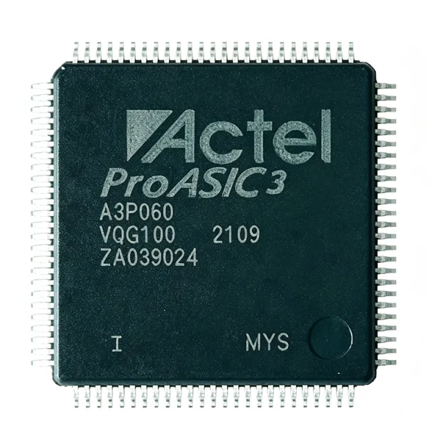
A3P060-TQ144
A3P060-TQ144 - 60K-Gate ProASIC3 FPGA | Microchip
Microchip Technology A3P060-TQ144 is a ProASIC3 flash-based field-programmable gate array with 60,000 system gates, 91 programmable I/O pins, and 18,432 RAM bits in a 144-pin TQFP package measuring 20 mm by 20 mm. The device uses CMOS logic and operates from a 1.5 V core supply, with the identified commercial-temperature configuration specified for 0°C to 70°C. Its surface-mount package supports compact embedded control, industrial automation, consumer electronics, and automotive-adjacent control systems where reprogrammable logic and a high pin count are useful.
A field-programmable gate array, or FPGA, is a programmable digital semiconductor that combines configurable logic blocks, programmable interconnect, and user I/O in one device. An FPGA belongs to the programmable-logic hierarchy alongside CPLDs, while offering greater logic density and more flexible routing than a basic low-complexity programmable device. The ProASIC3 family combines flash configuration, reusable silicon, and field programmability to support design revisions, production configuration, and logic updates without changing the PCB.
The A3P060 provides 60,000 system gates, 91 user-programmable I/O pins, and 18,432 RAM bits. These figures make it suitable for control logic, interface bridging, protocol conversion, embedded state machines, and multi-channel signal conditioning. Its 144-pin TQFP footprint exposes substantially more I/O than a small FPGA package, allowing parallel buses, counters, capture logic, and multiple external interfaces to be consolidated on a single device.
The device is manufactured in CMOS technology and belongs to the ProASIC3 flash FPGA family. Its architecture places configurable logic and routing resources between programmable I/O, enabling implementation of synchronous and asynchronous digital systems. Unlike a mask-programmed ASIC, the FPGA can be configured after manufacture, shortening prototype cycles and enabling one board design to support several firmware or logic revisions. The 1.5 V core architecture should be paired with the power-supply and decoupling network specified by the manufacturer.
Typical applications include industrial factory controllers, sensor and monitoring interfaces, consumer control boards, automotive accessory controllers, and compact embedded systems requiring numerous parallel I/O. A design can place the A3P060 between sensors or actuators and a higher-level processor, using its programmable logic for protocol conversion, timing, filtering, and data capture. The same pin-compatible approach also supports controlled migration among qualified ProASIC3 speed, package, and temperature configurations.
PCB design should preserve the manufacturer's recommended power, ground, clock, and configuration arrangements. Place decoupling capacitors close to the supply pins, provide a stable clock source with the required signal integrity, and leave programming and configuration access available for manufacturing and field updates. Verify every signal against the pin-assignment table for the exact ordering code before releasing the layout.
This product record combines the exact A3P060-TQ144 ordering information with package, resource, temperature, voltage, and I/O characteristics, plus a pin-to-pin replacement assessment and practical selection guidance. It is intended to accelerate schematic review, PCB compatibility checks, sourcing, and design-in decisions for ProASIC3-based systems.
RFQ
رابطہ