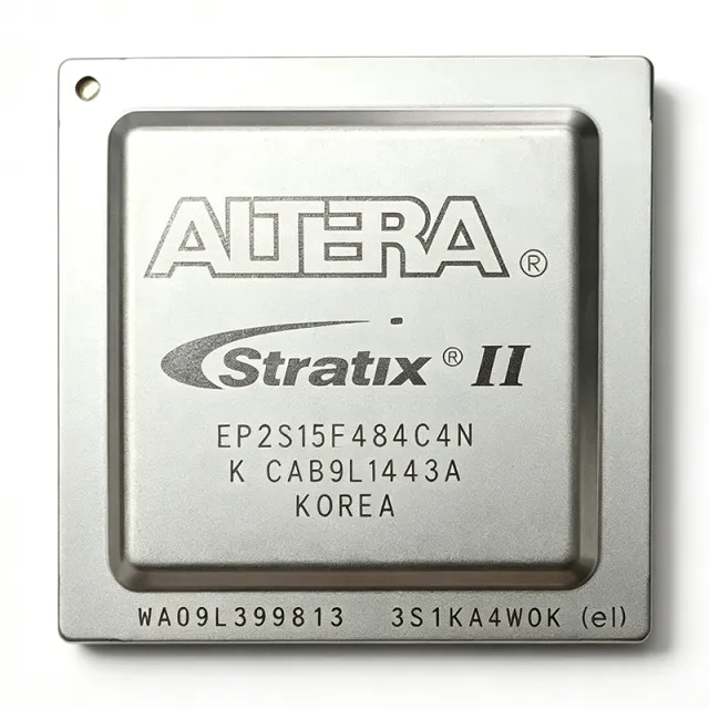
EP2S180F1020C3
EP2S180F1020C3 - Stratix II 180K LEs FPGA, 1020-BGA | Intel
The Intel (formerly Altera) EP2S180F1020C3 is a high-density Stratix II Field Programmable Gate Array (FPGA) IC built on a 1.2 V, 90 nm, all-layer copper SRAM process, delivering approximately 179,400 equivalent logic elements (LEs), 9,383,040 RAM bits, and 742 user I/Os in a 1020-ball flip-chip BGA package. It belongs to the EP2S180 device class, the largest density member of the Stratix II family, and is positioned for performance-critical digital signal processing, communications infrastructure, and high-throughput parallel processing designs.
An FPGA (Field Programmable Gate Array) is a reconfigurable integrated circuit containing an array of programmable logic blocks, interconnect, and dedicated silicon resources such as block RAM, DSP blocks, and high-speed transceivers. Unlike fixed-function ASICs, FPGAs can be re-programmed in the field via a hardware description language (HDL) such as VHDL or Verilog, making them ideal for prototyping, low-volume production, and designs that require late-stage or in-system logic changes. The Stratix II family sits within Intel's broader programmable logic hierarchy: FPGA -> Programmable Logic -> Logic Device -> Semiconductor, and is widely used in telecom, defense, and high-performance computing applications.
Key features of the EP2S180F1020C3 include approximately 8,970 LABs (Logic Array Blocks), 9 Mbit of embedded TriMatrix memory, dedicated DSP blocks for high-speed multiplication, and up to 742 user I/Os. The device supports multiple high-speed I/O standards including LVDS, LVPECL, SSTL, and HSTL, enabling interface to DDR/DDR2 memory, LVDS links, and backplane transceivers. The C3 speed grade and commercial temperature rating make it suitable for cost-optimized, lab-grade, and indoor equipment designs rather than automotive or extended-industrial environments.
The architecture uses Adaptive Logic Modules (ALMs) - each ALM contains a combination look-up table (LUT), two programmable registers, and dedicated adder circuitry, providing approximately 180,000 equivalent LEs while consuming roughly 40% less area and power than the original Stratix architecture. The device integrates dedicated DSP blocks capable of operating at hundreds of MHz and supports high-speed external memory interfaces including DDR2 SDRAM, QDRII SRAM, and RLDRAM II. The 1020-pin BGA package exposes extensive parallel I/O for memory, chip-to-chip interconnect, and parallel sensor or data acquisition buses.
Typical applications include high-performance DSP (radar, software-defined radio, baseband processing), telecommunications line cards and switches, ASIC prototyping and emulation, high-speed data acquisition systems, and parallel compute accelerators. When designing with this device, designers should use the Quartus II (now Quartus Prime) development toolchain for synthesis, place-and-route, and timing closure. Designers should also evaluate thermal dissipation carefully: at full utilization the EP2S180 can dissipate tens of watts, and the flip-chip BGA requires a properly designed PCB stack-up with adequate thermal vias and copper area to keep junction temperature within specification.
This page synthesizes distributor pricing, drop-in same-package alternatives, and practical design considerations not found in the manufacturer datasheet. Where parameters were not directly listed in the source search results, [DATA_NEEDED] markers are used to avoid fabrication; engineers should consult the official Stratix II datasheet and the device handbook for definitive electrical characteristics.
RFQ
رابطہ