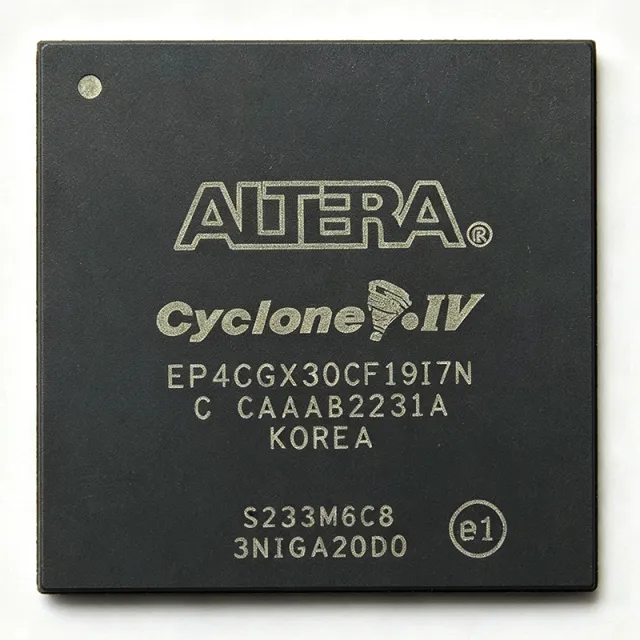
EP4CGX30CF19C6N
EP4CGX30CF19C6N - Cyclone IV GX FPGA, 29K LE, 150 I/O, 324-FBGA | Intel / Altera
The Intel / Altera EP4CGX30CF19C6N is a low-power, low-cost Cyclone IV GX Field Programmable Gate Array (FPGA) fabricated on a 60 nm process, offering 29,440 logic elements, 1,105,920 bits of embedded memory, and 150 user I/O pins housed in a 324-ball FineLine BGA (FBGA) package. The device integrates up to eight integrated 3.125 Gbps transceivers, hardware multipliers, and a rich set of memory interfaces, targeting cost-sensitive applications that still require high-speed serial connectivity. It belongs to the Cyclone IV GX family and operates from a 1.2 V core supply with a commercial temperature grade of 0 °C to 85 °C.
A Field Programmable Gate Array (FPGA) is a reprogrammable semiconductor device in the programmable logic family, sitting hierarchically between application-specific integrated circuits (ASICs) and general-purpose processors in terms of flexibility, performance per watt, and unit cost. FPGAs are widely used for digital signal processing, hardware acceleration, custom peripheral interfacing, and rapid prototyping of parallel compute pipelines. The Cyclone IV GX family specifically combines the low static and dynamic power of the Cyclone IV architecture with integrated high-speed transceivers, a combination not previously available in low-cost FPGA families.
Key features of the EP4CGX30CF19C6N include 29,440 logic elements (LEs), 66 embedded 18 x 18 multipliers for DSP, 1,105,920 bits (135 Kb) of on-chip RAM configured as M9K blocks, four general-purpose PLLs, and 150 single-ended or 75 differential-pair user I/Os. The device supports LVDS, SSTL, HSTL, and LVPECL I/O standards, and the integrated transceivers operate from 600 Mbps to 3.125 Gbps across protocols including PCI Express Gen1, Gigabit Ethernet, Serial RapidIO, and CPRI. The configuration scheme supports both passive serial (AS) and JTAG programming.
The Cyclone IV GX architecture combines a logic fabric of LABs (logic array blocks) with embedded memory, multipliers, and transceivers on a single die. Designers compile HDL or schematic designs into a bitstream using Quartus II software and load the bitstream into SRAM-based configuration cells. The device supports hot-socketing and partial reconfiguration in select modes, enabling dynamic hardware updates in deployed systems.
Typical applications include industrial video and image processing, motor control and drive subsystems, low-cost protocol bridging (PCIe, GbE, CPRI), portable and battery-powered test equipment, and machine-vision camera interfaces. Its balance of logic density, transceiver count, and static power makes it particularly attractive for cost-sensitive designs that nonetheless need multi-gigabit serial links.
Design considerations include careful PCB layout of the 324-ball FBGA, decoupling of the 1.2 V core and 2.5 V/3.3 V auxiliary rails, and routing of the high-speed transceiver channels with controlled-impedance differential pairs (typically 100 ohm). Quartus II software handles synthesis, place-and-route, and timing closure. For cost-down variants, the Cyclone IV E family (no transceivers) and Cyclone V (next-generation) families are alternative architecture families within the Altera / Intel portfolio.
This page consolidates distributor pricing as of 2026-09-10, drop-in alternative MPNs, and engineering design notes that go beyond the bare manufacturer datasheet, providing practical guidance for hardware engineers evaluating the EP4CGX30CF19C6N for new designs.
RFQ
رابطہ