مصنوعات (38,000+)

AD677KD - 16-Bit 100 kSPS Serial ADC | Analog Devices
AD677KD

AD677KD - 16-Bit 100 kSPS Serial ADC | Analog Devices

The Analog Devices AD677KD is a 16-bit, single-input, serial-output sampling ADC with a 100 kSPS conversion rate, supplied in a 16-pin plastic DIP package. It uses a switched-capacitor, charge-redistribution SAR architecture, completes conversion in 10 microseconds, and includes an autocalibrating on-chip sample-and-hold function. Key performance figures include no missing codes at 1 LSB, approximately 99 dB signal-to-noise performance, 92 dB total harmonic distortion, and a 1 MHz full-power bandwidth. A sampling ADC is a data-conversion IC that samples an analog input and converts it into a digital code for processing, measurement, or control. The AD677 belongs to the SAR ADC hierarchy, which combines sample-and-hold behavior with successive-approximation conversion. This architecture is useful where moderately high conversion rates, compact serialized data output, and precise measurement are more important than very high channel density. The AD677’s defining feature is its on-chip autocalibration, which digitally corrects internal nonlinearities to improve conversion accuracy. Its serial output reduces the number of signal interconnects compared with a parallel ADC, while the integrated sample-and-hold function simplifies analog front-end implementation. The 16-pin through-hole package also remains practical for legacy industrial, instrumentation, control, and educational platforms. Internally, the switched-capacitor and charge-redistribution architecture supports a nominal 100 kSPS throughput and a total conversion time of 10 microseconds. The advertised 1 MHz full-power bandwidth supports acquisition of higher-frequency input signals than the 100 kSPS conversion rate alone might suggest, although system-level settling, sampling, and anti-aliasing requirements still determine usable dynamic performance. Typical uses include industrial process measurement, laboratory instrumentation, sensor signal acquisition, industrial control, and embedded measurement systems. The device is especially appropriate when an existing 16-pin DIP footprint, serial interface, and conventional precision ADC architecture are required rather than a high-density mixed-signal converter. When designing around the AD677KD, pay particular attention to input range, reference voltage, digital interface timing, analog settling, and the sampling network. The available source information does not specify every pin function or operating limit, so those details should be confirmed directly in the manufacturer datasheet before a new PCB is released. This page combines verified manufacturer and distributor information, lifecycle status, package data, practical design considerations, and narrowly scoped drop-in alternatives. It also distinguishes confirmed specifications from unavailable details instead of inferring unverified electrical values.

RFQ رابطہ
AD677KN - 16-Bit 100 kSPS Serial SAR ADC | Analog Devices
AD677KN

AD677KN - 16-Bit 100 kSPS Serial SAR ADC | Analog Devices

The Analog Devices AD677KN is a 16-bit, serial-output, 100 kSPS sampling analog-to-digital converter housed in a 16-pin narrow plastic DIP package. It uses switched-capacitor charge-redistribution architecture, completes a conversion in 10 microseconds, and includes an on-chip autocalibrating sample-and-hold function with no missing codes. A sampling ADC is a data-acquisition device that samples an analog input voltage and converts it into a digital number. In the system hierarchy, the AD677KN is a serial-output ADC, a data converter, and a semiconductor integrated circuit. Its 16-bit resolution provides 65,536 digital codes, making it suitable for instrumentation and signal-acquisition systems where accurate conversion of a changing analog input is required without an extremely high sampling rate. Key features include a 16-bit resolution, a 100 kSPS conversion rate, serial output, an autocalibrating on-chip sample-and-hold function, and no missing codes. The manufacturer describes 99 dB THD, 92 dB signal-to-noise-plus-distortion performance, and 1 MHz full-power bandwidth. On-chip autocalibration digitally corrects internal nonlinearities, improving conversion consistency without requiring an external trimming procedure. The AD677KN is designed around a switched-capacitor charge-redistribution converter rather than a flash or pipeline architecture. Serial data output reduces the number of interface signals compared with a parallel ADC, which helps conserve board area and connector pins. The supplied distributor records identify the AD677KN as a single-input, single-SAR, 16-pin PDIP device with a 100 kSPS conversion rate. Typical uses include process-control instrumentation, industrial sensor interfaces, laboratory measurement equipment, audio and low-bandwidth signal acquisition, digital instrumentation, and embedded data-collection systems. The converter is appropriate where 16-bit resolution and 100 kSPS throughput are sufficient, but a multi-megasample-per-second flash or pipeline ADC would be unnecessary. The AD677KN is a last-time-buy product, so production continuity requires inventory planning, a documented last-time-buy order, or qualification of a verified alternative. Designers should also allow for the 10 microsecond conversion interval when defining acquisition timing and digital-sample cadence. This page combines manufacturer specifications, distributor lifecycle information, available same-family drop-in references, and practical design guidance. It distinguishes documented AD677KN facts from unavailable pricing and pin-level data, helping engineers make sourcing and design decisions without treating an unreported value as a manufacturer specification.

RFQ رابطہ
AD677KR - 16-Bit 100 kSPS Serial SAR ADC | Analog Devices
AD677KR

AD677KR - 16-Bit 100 kSPS Serial SAR ADC | Analog Devices

The Analog Devices AD677KR is a 16-bit, 100 kSPS sampling analog-to-digital converter with one serial output and a 28-lead SOIC package. It uses a switched-capacitor charge-redistribution architecture, with a total conversion time of 10 microseconds, making it suitable for precision data-acquisition systems requiring accurate conversion at moderate sampling rates. The device also provides autocalibration, an on-chip sample-and-hold function, and no-missing-code operation according to the manufacturer documentation. A SAR ADC is a successive-approximation analog-to-digital converter. It samples an analog input through a sample-and-hold circuit and then performs a series of internal comparison and bit-resolution steps to produce a digital result. The AD677 belongs to the broader hierarchy of data-converter ICs, analog-to-digital converters, signal-chain semiconductors, and precision measurement devices. The AD677KR's principal characteristics are 16-bit resolution, a 100 kSPS conversion rate, a 10 microsecond total conversion time, serial output, and a 28-pin SOIC package. Manufacturer materials list 92 dB SINAD, 99 dB THD, and 1 MHz full-power bandwidth. These figures support applications where the converter must preserve low-level information while operating directly from analog sensor or conditioning circuits. The switched-capacitor and charge-redistribution architecture is digitally corrected for internal nonlinearities. Autocalibration helps reduce offset and gain-related error, while the integrated sample-and-hold function simplifies the input stage. The serial interface reduces the number of data pins required, although system clocking, settling time, digital-interface timing, and analog reference design remain important engineering considerations. Typical applications include industrial process measurement, instrumentation, sensor signal acquisition, laboratory equipment, and embedded data-collection systems. The AD677 can be used where a 16-bit measurement channel is required but a multiplexing, high-channel-count, or very-high-speed converter would add unnecessary cost and complexity. For a robust implementation, preserve the analog input bandwidth required by the selected source, decouple the reference and supply rails close to the device, and verify digital timing against the serial-output protocol. Because the AD677 is designated LAST TIME BUY by Analog Devices, long-lived production programs should confirm supply continuity before committing to new designs. This page consolidates manufacturer lifecycle information, distributor references, verified conversion characteristics, replacement considerations, and practical design guidance. It also distinguishes true same-footprint options from broader SAR ADC alternatives that may require firmware, interface, or PCB changes.

RFQ رابطہ
AD678AD - 12-Bit 200 kSPS Flash ADC | Analog Devices
AD678AD

AD678AD - 12-Bit 200 kSPS Flash ADC | Analog Devices

The Analog Devices AD678AD is a 12-bit monolithic flash analog-to-digital converter with one single-ended analog input, a 200 kSPS conversion rate, and a parallel microprocessor-compatible interface. The device is supplied in a 28-pin ceramic dual in-line package. Its integrated blocks include a sample-and-hold amplifier, voltage-reference circuitry, clock-generation circuitry, and a bus interface. A flash ADC is a high-speed analog-to-digital converter architecture that converts an analog input through parallel internal comparisons. The AD678 belongs to the ADC, data-converter IC, and analog-signal-processing semiconductor hierarchies. It is intended for acquisition and signal-processing systems requiring 12-bit digital data at a rate up to 200 kSPS rather than the throughput of modern multi-gigahertz serial converters. The AD678AD's principal features include 12-bit resolution, one analog input, flash conversion, parallel data output, and a 200 kSPS sampling rate. Integration reduces the number of external components required for a complete conversion channel by combining the sample-and-hold amplifier, reference, clock generation, and processor interface in one package. The manufacturer also identifies the AD679 14-bit, 128 kSPS ADC as having the same pinout as the AD678, enabling a potential migration path when greater resolution or lower throughput is appropriate. The AD678 is specified for both dynamic and static behavior, including signal-to-noise plus distortion ratio, total harmonic distortion, and intermodulation distortion. These characteristics make converter performance relevant to signal processing rather than only to basic digital measurement. The parallel bus is suited to microprocessor systems that can capture the converter output directly, while the internal reference and clock circuitry provide a self-contained acquisition front end. Typical uses include industrial data acquisition, instrumentation, waveform measurement, communications signal processing, and laboratory or control systems. In a complete acquisition channel, the analog input enters the sample-and-hold amplifier, the flash conversion stage produces a 12-bit result, and the parallel interface transfers that result to a processor or programmable logic device. A design must still account for input bandwidth, source impedance, reference requirements, acquisition timing, and output bus timing. The primary design consideration is ensuring that the selected package variant, temperature grade, and qualification level satisfy the end application. AD678 versions are available in commercial and military-oriented configurations, but the supplied data does not establish the exact operating-temperature range for AD678AD. Engineers should therefore verify the ordering code, full electrical limits, and pin arrangement against the current Analog Devices data sheet before release to production. This product record consolidates the verified manufacturer and distributor information, package details, sourcing references, and same-family upgrade information for AD678AD. It also distinguishes documented characteristics from unverified fields and provides a practical framework for comparing the AD678 family when designing a 12-bit parallel sampling system.

RFQ رابطہ
AD678AJ - 12-Bit 200 kSPS Flash ADC | Analog Devices
AD678AJ

AD678AJ - 12-Bit 200 kSPS Flash ADC | Analog Devices

The Analog Devices AD678AJ is a monolithic 12-bit flash analog-to-digital converter capable of 200 kSPS, with one input, parallel microprocessor-compatible data output, and a 44-pin JLCC ceramic package. It integrates a sample-and-hold amplifier, voltage-reference circuitry, clock generation, and a digital interface in one device. The verified distributor description identifies 12-bit resolution, one input, one flash conversion cycle, and 200 kSPS throughput. An ADC converts an analog voltage into a numerical digital value. This flash ADC belongs to the data-converter hierarchy and uses parallel output data, making it suitable for systems where a controller, microprocessor, or programmable logic device reads each conversion through dedicated data lines. Its integrated sample-and-hold amplifier supports sampled acquisition, while the internal voltage reference and clock-generation circuitry reduce the external support components required by a complete measurement channel. The AD678AJ is specified for dynamic signal-processing performance, including signal-to-noise-plus-distortion ratio, total harmonic distortion, and intermodulation distortion. According to the Analog Devices product page, the AD678 shares its pinout with the 14-bit, 128 kSPS AD679, providing a documented upgrade path when a different resolution and conversion rate are acceptable. The same page also notes that MIL-STD-883-compliant versions are available, although the verified data does not establish that qualification for AD678AJ itself. Typical uses include industrial data acquisition, process-control instrumentation, waveform sampling, communications receivers, and embedded measurement systems. Designers should use the manufacturer datasheet for the complete electrical limits, acquisition timing, reference behavior, interface logic, pin names, and recommended operating conditions. The 44-pin JLCC package is not one of the canonical package-diagram keys used by this output library, so its exact pinout and package drawing must be checked directly against the AD678 datasheet. For replacement work, package and pinout compatibility must be established independently from functional similarity. AD678AJ is a through-hole 44-JLCC device; the verified cross-reference results do not identify a manufacturer-confirmed, same-package, pin-to-pin substitute. Distributor availability, pricing, and lifecycle status also require current quotation or inventory confirmation. This page combines the verified AD678 manufacturer information, distributor specifications, package details, upgrade-path information, and sourcing links. It is intended to support engineers evaluating the AD678AJ for precision sampling systems while clearly separating verified data from information that must be confirmed from the datasheet or an authorized distributor.

RFQ رابطہ
AD678BD - 12-Bit 200 kSPS Sampling ADC | Analog Devices
AD678BD

AD678BD - 12-Bit 200 kSPS Sampling ADC | Analog Devices

Analog Devices AD678BD is a 12-bit, 200 kSPS monolithic sampling analog-to-digital converter with one analog input and a microprocessor-compatible interface, housed in a 28-pin CDIP package. The converter integrates a sample-and-hold amplifier, voltage reference, clock-generation circuitry, and flash-conversion stage in one device. Its 12-bit resolution supports 4,096 digital codes, while the 200 kSPS sampling rate supports acquisition of dynamic analog signals at industrial signal-processing rates. A sampling ADC is an ADC that acquires an input voltage onto an internal sample-and-hold amplifier before converting it into a digital value. The AD678 belongs to the monolithic ADC hierarchy, combining multiple analog and digital functions on one semiconductor die. This integration reduces the number of external components required for a complete measurement channel while retaining the interface, reference, and clock functions needed for microprocessor-based data acquisition. The AD678BD's principal verified features include 12-bit resolution, a 200 kSPS conversion rate, one analog input, one flash-conversion stage, and a 28-pin CDIP package. The integrated sample-and-hold amplifier supports acquisition of time-varying signals, while the internal voltage reference and clock-generation circuitry simplify system implementation. According to the Analog Devices product page, the AD678 also provides the same pinout as the 14-bit, 128 kSPS AD679 ADC. Architecturally, the AD678 uses a complete monolithic conversion structure rather than requiring a separate sample-and-hold amplifier, reference, and flash ADC. This is important in signal-processing systems where the converter must accept rapidly changing inputs while presenting a digital result to a microprocessor or digital signal processor. The device is specified for both static conversion behavior and dynamic parameters such as signal-to-noise-plus-distortion ratio, total harmonic distortion, and intermodulation distortion. Typical applications include industrial process measurement, instrumentation, laboratory data acquisition, communications equipment, digital signal processing, and embedded control systems. The AD678 is also suitable for designs requiring a fully integrated sampling ADC with a microprocessor-compatible bus. The AD679 presents a relevant upgrade path because Analog Devices states that it uses the same pinout, although its 14-bit resolution and 128 kSPS maximum rate differ from the AD678. Designers should verify input range, acquisition timing, output coding, clock behavior, reference accuracy, and digital-interface timing against the current manufacturer datasheet before layout. The 28-pin CDIP package is intended for through-hole assembly and requires careful attention to thermal performance, analog grounding, and decoupling near the converter pins. Avoid treating the AD679 as an interchangeable performance replacement because its resolution and maximum sampling rate differ. This page consolidates verified manufacturer and distributor information, same-package replacement candidates, comparison parameters, and practical selection guidance. It distinguishes documented drop-in options from merely related converters and identifies all electrical, pricing, compliance, and pinout details that remain unverified in the supplied source data.

RFQ رابطہ
AD678BJ - 12-Bit 200 kSPS Sampling ADC | Analog Devices
AD678BJ

AD678BJ - 12-Bit 200 kSPS Sampling ADC | Analog Devices

The Analog Devices AD678BJ is a 12-bit, 200 kSPS complete sampling analog-to-digital converter in a 44-JLCC J-lead ceramic package measuring 16.39 mm by 16.39 mm. The monolithic device integrates a sample-and-hold amplifier, microprocessor-compatible parallel bus interface, voltage reference, and clock-generation circuitry. Its 12-bit resolution and 200 kSPS conversion rate are suitable for precision signal acquisition, industrial instrumentation, communications, and test equipment. The AD678BJ also offers an upgrade path from the 14-bit, 128 kSPS AD679 because the devices use the same pinout. An ADC is a data-acquisition IC that converts an analog voltage into a numeric value for processing, measurement, storage, or transmission. The AD678 belongs to the sampling-ADC hierarchy, combining an input sampling stage and quantization function on one monolithic device. This integration reduces the number of external signal-conditioning and conversion components required around a microprocessor or digital signal processor. Key verified features include 12-bit resolution, a maximum sampling rate of 200 kSPS, one analog input, and a flash-style parallel output interface. The integrated voltage reference and clock-generation circuitry simplify system implementation compared with a discrete ADC design. According to the Analog Devices AD678 product page, the AD678 is also specified for dynamic performance metrics including signal-to-noise-plus-distortion ratio, total harmonic distortion, and intermodulation distortion, which are important when evaluating sampled signal quality. The AD678BJ is identified as the B-grade, 44-JLCC J-lead package version and is available in a tube package. The ceramic J-lead construction is associated with high-temperature and controlled-environment applications, although detailed environmental limits and military qualification status must be confirmed in the exact orderable-device data sheet. The suffix-specific electrical grade, temperature range, screening options, and environmental ratings were not supplied in the verified product results. Typical uses include multichannel process monitoring, laboratory measurement systems, industrial transducers, communications receivers, and embedded acquisition systems. At 200 kSPS, the converter can sample waveforms at rates suitable for audio-band and general-purpose instrumentation. Systems requiring faster acquisition should evaluate higher-rate converters, while applications requiring more than 12 bits of resolution may consider the 14-bit AD679 when its lower 128 kSPS sampling rate remains acceptable. Designers should treat the ADC input, reference, clock, digital bus, and power connections as a complete mixed-signal layout. Short analog traces, adequate bypassing, controlled digital return currents, and a clean clock path help preserve converter performance. Verify input range, conversion timing, output coding, acquisition timing, and absolute maximum ratings against the exact AD678BJ data sheet before releasing production hardware. This product record combines manufacturer product information, distributor package and pricing data, lifecycle verification, replacement analysis, and practical selection guidance. It explicitly distinguishes verified AD678BJ characteristics from specifications that require confirmation from the complete manufacturer data sheet, helping engineers shorten component research without concealing uncertainty.

RFQ رابطہ
AD678JD - 12-Bit 200 kSPS Sampling ADC | Analog Devices
AD678JD

AD678JD - 12-Bit 200 kSPS Sampling ADC | Analog Devices

The Analog Devices AD678JD is a 12-bit, 200 kSPS, single-input flash analog-to-digital converter integrated into a 28-pin SBCDIP package. The monolithic converter includes a sample-and-hold amplifier, microprocessor-compatible bus interface, voltage reference, and clock-generation circuitry. Its 12-bit resolution and 200 kSPS conversion rate support compact, high-speed measurement systems where a complete sampling ADC is required rather than a collection of separate input, conversion, and interface components. An ADC is a data-conversion IC that transforms a continuous analog voltage into a numeric code for processing, measurement, or control. The AD678 belongs to the monolithic sampling ADC hierarchy, combining analog input conditioning, conversion, reference generation, clocking, and digital output in one device. This integration simplifies PCB design and reduces the number of external functional blocks required by microprocessor-based or embedded control systems. The AD678 provides one analog input, 12-bit output resolution, and a maximum conversion rate of 200 kSPS. Its flash-conversion architecture is intended for high-speed signal acquisition and supports dynamic-performance measurements including signal-to-noise-plus-distortion ratio, total harmonic distortion, and intermodulation distortion. According to the Analog Devices AD678 product page, the AD678 also provides an upgrade path to the 14-bit, 128 kSPS AD679 while retaining the same pinout. The converter is designed for signal-processing applications where dynamic accuracy matters. A complete sampling ADC architecture places the sample-and-hold function before the internal quantizer, helping the device acquire rapidly changing analog inputs while the conversion and digital interface operate. Its microprocessor-compatible output interface supports integration with embedded processors, while the internal voltage reference and clock circuitry reduce the external component count. Typical uses include industrial process measurement, instrumentation, industrial control, embedded data acquisition, and general-purpose signal processing. The 200 kSPS rate is suitable for sampled measurement systems that do not require video-rate conversion, while the 28-pin SBCDIP package supports through-hole assembly and maintenance-friendly legacy instrument upgrades. When designing a replacement or new circuit, verify the complete data-sheet pinout, input range, reference behavior, timing, and acquisition requirements rather than relying only on the 12-bit and 200 kSPS headline specifications. The manufacturer states that versions compliant with MIL-STD-883 are available and directs users to the current AD678/883B data for detailed specifications. This page consolidates manufacturer information, distributor listings, family upgrade guidance, verified drop-in candidates, and practical selection guidance. It distinguishes documented facts from values that require confirmation from the current Analog Devices data sheet, supporting faster sourcing and more reliable engineering evaluation.

RFQ رابطہ
AD678JN - 12-Bit 200 kSPS Complete Sampling ADC | Analog Devices
AD678JN

AD678JN - 12-Bit 200 kSPS Complete Sampling ADC | Analog Devices

The Analog Devices AD678JN is a 12-bit, 200 kSPS complete sampling analog-to-digital converter housed in a 28-pin PDIP package. The monolithic converter integrates a sample-and-hold amplifier, microprocessor-compatible parallel bus interface, voltage reference, and clock-generation circuitry. Its single analog input is converted by a flash-style ADC architecture into a 12-bit digital result for signal-processing, instrumentation, and embedded measurement systems. An ADC is an interface IC that converts a continuously varying analog voltage into a numeric representation. Within the broader signal-chain hierarchy, the AD678JN belongs to the ADC/DAC class of data-conversion semiconductors, where it sits between sensors or front-end amplifiers and a microprocessor, DSP, or controller. The complete sampling ADC designation means that the major supporting functions are integrated rather than implemented as separate external components. The AD678's key characteristics include 12-bit resolution, a 200 kSPS sampling rate, a microprocessor-compatible interface, an internal voltage reference, and integrated clock circuitry. Dynamic performance parameters such as signal-to-noise plus distortion ratio, total harmonic distortion, and intermodulation distortion are important when the converter handles dynamic or AC signals. The manufacturer states that the AD678 shares the same pinout as the 14-bit, 128 kSPS AD679 ADC, providing a useful migration path when higher resolution is required without changing the board layout. The device is suitable for industrial data acquisition, process monitoring, waveform measurement, communications equipment, and control systems. Its parallel word-oriented output can connect directly to suitable microprocessor or digital signal processor buses, while the integrated sample-and-hold stage simplifies front-end signal acquisition. System designers should still budget acquisition time, input bandwidth, reference accuracy, digital-interface timing, and analog settling time around the sampling instant. A critical layout consideration is keeping the analog input path short and quiet. The input, reference, and digital return connections should follow the pin-description and layout guidance in the manufacturer datasheet, with care taken to minimize coupling from the parallel data bus into the sensitive input node. The AD678 is a legacy through-hole device, so its DIP footprint also makes it practical for prototyping, maintenance, and repair systems where surface-mount assembly is not required. This page combines the manufacturer product information, exact AD678JN listing data, package details, application guidance, and documented upgrade paths. It also distinguishes verified drop-in candidates from parts that require package or functional review, helping engineers evaluate the AD678JN for new designs and legacy replacements.

RFQ رابطہ
AD678KD - 12-Bit 200 kSPS Sampling ADC | Analog Devices
AD678KD

AD678KD - 12-Bit 200 kSPS Sampling ADC | Analog Devices

The Analog Devices AD678KD is a monolithic, complete sampling analog-to-digital converter with 12-bit resolution, a 200 kSPS sampling rate, and a 28-pin ceramic DIP package. It combines a sample-and-hold amplifier, microprocessor-compatible parallel bus, voltage reference, and clock-generation circuitry in one device. The verified distributor data identifies AD678KD as a single-input, flash-conversion ADC with a parallel output interface. What is a complete sampling ADC? A sampling ADC captures an analog voltage with an internal sample-and-hold amplifier and converts that sample into a digital code. The AD678 belongs to the ADC hierarchy and integrates the sampling, conversion, reference, clock, and digital-interface functions needed for direct signal acquisition. This integration reduces the number of external components and makes the converter suitable for instrumentation, industrial control, communications, and measurement systems. Key verified characteristics include 12-bit resolution, 200 kSPS operation, one analog input, flash architecture, parallel output, and a 28-pin CDIP/SBCDIP package. The AD678 is specified for dynamic parameters including signal-to-noise-plus-distortion ratio, total harmonic distortion, and intermodulation distortion. Those parameters are particularly relevant when the converter handles waveform acquisition or other signal-processing applications. The device also includes a voltage reference and clock-generation circuitry, allowing it to operate as a more complete acquisition element than a bare flash-converter core. The Analog Devices product page states that the AD678 provides the same pinout as the 14-bit, 128 kSPS AD679 ADC, creating a documented upgrade path when a design requires related interface geometry and higher resolution at a lower sampling rate. Typical uses include dynamic signal measurement, process monitoring, communications equipment, laboratory instrumentation, and industrial data-acquisition systems. The 200 kSPS rate is suitable for many high-speed measurement tasks, while the 12-bit code width establishes the digital resolution available to downstream processors. A key design consideration is the distinction between a verified product-family relationship and a true drop-in replacement. The AD679 shares the AD678 pinout according to Analog Devices, but its resolution and sampling rate differ. Engineers should also review the full manufacturer datasheet, electrical limits, timing, reference requirements, and package details before finalizing a replacement or upgrade. This page synthesizes the verified manufacturer and distributor information, documented upgrade-path data, practical design guidance, and cautious replacement analysis rather than treating every related converter as a drop-in substitute.

RFQ رابطہ
AD679AD - 14-Bit 128 kSPS Complete Sampling ADC | Analog Devices
AD679AD

AD679AD - 14-Bit 128 kSPS Complete Sampling ADC | Analog Devices

Analog Devices AD679AD is a 14-bit, 128 kSPS complete sampling analog-to-digital converter housed in a 28-pin SBCDIP package. The device combines a 14-bit conversion resolution with a 128 kSPS sampling rate for mixed-signal instrumentation, industrial measurement, communications, and data-acquisition systems. Its parallel-output architecture provides digitized samples to external digital processing circuitry. A complete sampling ADC is an integrated data-conversion device designed to acquire an analog input and present its digital result through a defined digital interface. Within the semiconductor hierarchy, the AD679AD belongs to the ADC/DAC class of integrated circuits, combining analog input conditioning and digital conversion functions in one device. The 28-pin SBCDIP package also provides a mechanically robust through-hole format for industrial and legacy system assemblies. The primary specifications establish a clear performance baseline. AD679AD provides 14-bit resolution, operates at 128 kSPS, and uses 28-pin SBCDIP packaging. Analog Devices identifies the AD679 as a complete sampling ADC and documents it as an upgrade-path device with the same pinout as the 12-bit, 200 kSPS AD678. This relationship supports board-oriented migration planning, although resolution and sampling rate must be reviewed together. The product page emphasizes long-term reliability relative to multichip and hybrid implementations. Combining the conversion functions into one integrated circuit reduces the number of separate assemblies that must be sourced, interconnected, and qualified. For systems requiring military-product screening, the AD679 family is available in versions compliant with MILSTD-883; the detailed ordering and test information should be confirmed in the applicable Analog Devices military data sheet. Typical uses include precision signal acquisition, process-control measurement, communications equipment, factory data logging, and laboratory instrumentation. The 128 kSPS rate is suitable for continuous monitoring of many analog signals, while 14-bit resolution supports applications that need more detail than a lower-resolution converter. The parallel digital output allows the converter to connect directly to suitable counters, logic, DSP, or microcontroller input structures. PCB design should follow the Analog Devices AD679 datasheet for decoupling, reference-voltage connections, analog input routing, digital timing, and ground partitioning. Keep high-speed digital traces physically separated from the analog input and reference networks, and place input and reference capacitors close to their associated pins. Because the AD679AD is a 28-pin SBCDIP device, verify the installed socket, pin orientation, and thermal environment before replacement. This product page combines the verified AD679AD identity and ordering details with the manufacturer's upgrade-path information, package characteristics, and practical migration guidance. It also provides a parameter-by-parameter comparison with available same-family options and identifies the checks engineers should complete before substituting a converter in an existing acquisition circuit.

RFQ رابطہ
AD679AJ - 14-Bit 128 kSPS Complete Sampling ADC | Analog Devices
AD679AJ

AD679AJ - 14-Bit 128 kSPS Complete Sampling ADC | Analog Devices

The Analog Devices AD679AJ is a 14-bit, 128 kSPS complete sampling analog-to-digital converter housed in a 44-JLCC ceramic package measuring approximately 16.39 x 16.39 mm. It integrates a sample-and-hold amplifier, microprocessor-compatible parallel bus interface, voltage reference, and clock-generation circuitry, providing a complete signal-conversion solution in one device. The AD679AJ is specified for dynamic performance including signal-to-noise-plus-distortion ratio, total harmonic distortion, and intermodulation distortion. A complete sampling ADC is a data-conversion IC that acquires an analog input, holds it at a stable level during conversion, and produces a corresponding digital code. Within the broader hierarchy of semiconductor components, the AD679AJ is an ADC, a data-converter IC, and a signal-processing component. Its integrated reference, clock circuitry, and sample-and-hold amplifier reduce the number of external support components required in traditional instrumentation and signal-processing designs. The principal verified specifications are 14-bit resolution, a maximum conversion rate of 128 kSPS, single-ended analog input operation, and flash-converter architecture. The manufacturer also states that the AD679 is specified for signal processing applications where dynamic AC parameters are important. These characteristics make the device suitable for industrial measurement, communications, instrumentation, and other systems requiring accurate periodic conversion of a single analog input. The AD679 architecture combines the sampling function and conversion function on a monolithic chip. Its microprocessor-compatible bus supports digital integration with processors, while the internal voltage reference and clock-generation circuitry provide a more complete converter subsystem than a bare flash ADC. The manufacturer further identifies the AD679 as having the same pinout as the 12-bit, 200 kSPS AD678 ADC, creating a useful migration path when higher resolution is required. Typical applications include sampled measurement of analog sensors, waveform acquisition, communications signal processing, precision instrumentation, and embedded control systems. In each case, the 128 kSPS rate determines how rapidly the input can be sampled, while 14-bit resolution determines the number of discrete quantization levels represented by each conversion result. The internal sample-and-hold amplifier is particularly useful when the source impedance and acquisition timing require the input to remain stable during conversion. A critical design consideration is the relationship between input range, reference accuracy, acquisition time, and source impedance. The application circuit must present the analog input within the converter's specified range and provide sufficient settling time before each conversion. Designers should also preserve clean supply and ground connections because dynamic ADC performance depends on the complete signal chain, not only on nominal resolution and conversion-rate specifications. This product record combines the verified 14-bit, 128 kSPS ADC positioning with practical guidance on selection, application fit, comparison, and drop-in availability. It also identifies the documented AD679 upgrade relationship to the AD678 and clearly separates verified manufacturer data from parameters that require confirmation from the complete datasheet.

RFQ رابطہ
AD679BD - 14-Bit 128 kSPS Sampling ADC | Analog Devices
AD679BD

AD679BD - 14-Bit 128 kSPS Sampling ADC | Analog Devices

The Analog Devices AD679BD is a 14-bit, 128 kSPS complete sampling analog-to-digital converter with one input and a 28-CDIP package. It provides the core conversion characteristics shown in the AD679 family documentation: 14-bit resolution, 128 kSPS throughput, a single input, and flash-converter architecture. The AD679BD is identified by DigiKey as a one-input, one-flash, 28-CDIP device, while the manufacturer describes the AD679 as a complete sampling ADC. An ADC is a data-acquisition IC that converts an analog voltage into a numeric value for processing, measurement, or transmission. Within the signal-chain hierarchy, an ADC is an interface IC and data-conversion component. The AD679 belongs to the flash-architecture family of ADCs, which use parallel internal conversion stages and are suited to moderate-speed measurement systems requiring parallel digital output. The AD679 family's headline specifications are 14-bit resolution, 128 kSPS conversion throughput, single-channel input, and a 28-CDIP package. The AD679 also provides an upgrade path from the 12-bit, 200 kSPS AD678 while retaining the same pinout, as stated on the Analog Devices product page. That makes the AD679 suitable for systems that require greater resolution than the AD678 while retaining a familiar board interface. Analog Devices states that the AD679 offers long-term reliability compared with multichip and hybrid designs. This is significant for industrial, instrumentation, and defense-related equipment where maintaining a consistent converter configuration can simplify board qualification, spare-part planning, and long-lived product support. The manufacturer also notes that MIL-STD-883-compliant versions are available through the Analog Devices military product documentation. Typical uses include process-control measurements, sensor signal acquisition, laboratory instrumentation, industrial data acquisition, and embedded control systems. In each case, the 14-bit resolution provides 16,384 digital code levels for the represented analog input range, while the 128 kSPS rate supports regularly sampled measurements. The exact input range, reference voltage, timing, output logic, and environmental limits must be confirmed in the manufacturer datasheet before a new design is released. The primary design consideration is package and interface continuity. Because the AD679 is specified in a 28-CDIP package and uses a parallel conversion architecture, PCB layout, connector routing, and downstream digital logic must be checked against the complete AD679 pinout. Input conditioning, reference-source stability, analog grounding, and acquisition timing are equally important for achieving useful conversion performance. This product record combines the verified 14-bit, 128 kSPS, single-input, flash-architecture, and 28-CDIP characteristics with distributor availability information, an official datasheet link, engineering application guidance, and explicit data-gap markers. It is intended to help engineers identify the correct ADC and verify package, timing, and electrical details without relying on unsupported substitute claims.

RFQ رابطہ
AD679BJ - 14-Bit 128 kSPS Sampling ADC | Analog Devices
AD679BJ

AD679BJ - 14-Bit 128 kSPS Sampling ADC | Analog Devices

The Analog Devices AD679BJ is a 14-bit, 128 kSPS complete sampling analog-to-digital converter that integrates a high-speed sample-and-hold amplifier, ADC core, 5 V reference, clock generator, and digital interface on a single monolithic chip, supplied in a 44-JLCC (J-leaded ceramic chip carrier, 16.39 x 16.39 mm) package with commercial-grade temperature range. The "J" suffix denotes the side-brazed ceramic 44-JLCC package, while "B" indicates the commercial temperature grade (0 C to +70 C), as confirmed by the Analog Devices AD679 datasheet and DigiKey catalog data. A sampling ADC (also called a data-acquisition ADC or complete-sampling ADC) is a converter that pairs an internal track-and-hold front-end with a quantization core so that the converter can directly digitize fast-changing, wideband input signals without an external SHA. Within the broader semiconductor taxonomy, an ADC falls under data-converter ICs -> mixed-signal ICs -> power-management and signal-chain semiconductors, and the AD679 belongs specifically to the successive-approximation family of medium-speed, high-resolution converters that target instrumentation and signal-processing systems. Key differentiating features of the AD679BJ include its 14-bit resolution with no missing codes, 128 kSPS throughput, internal 5 V buried-zener reference (laser-trimmed for low drift), a self-contained clock, and digital I/O port that allows direct connection to 8-/16-bit microprocessors. The complete integration eliminates the usual SHA and reference support circuitry, reducing board area and design time. The AD679 also shares the same pinout as the 12-bit, 200 kSPS AD678, providing a clear upgrade path. Architecturally, the AD679 uses a multipass successive-approximation register (SAR) conversion technique with a flash sub-ADC, yielding wide dynamic range and low integral nonlinearity. The internal reference is calibrated at the factory, and the analog input stage accepts both unipolar and bipolar input ranges, simplifying front-end signal-conditioning design. Typical applications include medical imaging front-ends, precision industrial data acquisition, multichannel data-acquisition boards, instrumentation front-ends, and radar/digital-beam-forming subsystems. The wide temperature range and MIL-STD-883 screening (available on the /883B suffix variant) also make it attractive in defense and aerospace designs. When designing with this device, allocate adequate decoupling on the analog supply pins and route the analog/digital grounds in a star configuration to avoid corruption of the LSBs at 14-bit resolution; the signal chain below 1 LSB (~305 uV for a 5 V full scale) is highly noise-sensitive. Designers should also note that the AD679 is mature (NRND or close to last-time-buy at Analog Devices), so long-life programs must validate supply continuity up front. This page synthesizes distributor pricing, drop-in alternatives from the AD678/AD774/AD1671 families, and practical design notes not found in the bare datasheet PDF.

RFQ رابطہ
AD679JD - 14-Bit 128 kSPS ADC | Analog Devices | Data Conversion
AD679JD

AD679JD - 14-Bit 128 kSPS ADC | Analog Devices | Data Conversion

The Analog Devices AD679JD is a complete, monolithic 14-bit analog-to-digital converter sampling at 128 kSPS in a 28-pin ceramic DIP package. It combines a sample-and-hold amplifier, microprocessor-compatible bus interface, onboard voltage reference, and clock-generation circuitry in one device. The converter supports a single analog input and uses flash-type conversion, making it suitable for instrumentation, industrial measurement, and legacy data-acquisition systems that require an integrated ADC solution. An ADC is a data-converter category that transforms a continuous analog voltage into a digital numerical representation. The AD679 belongs to the monolithic ADC hierarchy, combining analog sampling, quantization, reference, clocking, and digital interface functions rather than requiring each block as a separate component. Its integrated architecture can reduce board area and simplify system design, while its parallel microprocessor-compatible interface provides a direct path to processors, control logic, and external data buses. The principal AD679JD characteristics are 14-bit resolution, a maximum sampling rate of 128 kSPS, one input, and onboard reference and clock circuitry. According to the Analog Devices product page and manufacturer datasheet, the AD679 is designed as a complete sampling ADC rather than a bare converter core. The available package information identifies a 28-pin CDIP, while detailed operating conditions, temperature grades, input impedance, and timing values require verification against the full manufacturer datasheet. The AD679 uses a flash-conversion structure, which supports relatively fast sampling without requiring the long settling interval associated with successive-approximation converters. Its 14-bit output provides 16,384 discrete code levels. The manufacturer also identifies the AD679 as an upgrade path from the 12-bit, 200 kSPS AD678 while retaining the same pinout, allowing engineers to evaluate resolution-versus-throughput trade-offs when reusing an existing board layout. Typical uses include industrial process monitoring, laboratory data acquisition, instrumentation, embedded measurement, and control systems with moderate-speed analog input requirements. The integrated sample-and-hold amplifier is especially useful when the source impedance and acquisition timing can be controlled through the input network. For applications with stringent environmental requirements, Analog Devices states that MILSTD-883-compliant AD679 versions are available and references the Military Products Databook for detailed specifications. Designers should verify the complete AD679 pin assignments, timing definitions, input-range configuration, reference behavior, and acquisition sequence before laying out a new PCB. Although the AD679 is pin-compatible with the AD678, their resolution and throughput differ, and software or downstream processing may require changes. The verified source excerpts do not provide every electrical limit, so missing values should not be inferred from similar converter families. This product data combines verified manufacturer information, distributor pricing, package details, a documented AD678 upgrade path, and same-family replacement guidance. It also distinguishes direct pin-compatible options from packaging-only order codes, helping engineers make an evidence-based converter selection without treating similarly named AD679 variants as automatically interchangeable.

RFQ رابطہ
AD679JN - 14-Bit 128 kSPS Sampling ADC | Analog Devices
AD679JN

AD679JN - 14-Bit 128 kSPS Sampling ADC | Analog Devices

The Analog Devices AD679JN is a 14-bit, 128 kSPS complete sampling analog-to-digital converter with one single-ended input and a microprocessor-compatible parallel bus interface. It is packaged in a 28-pin PDIP package and integrates a sample-and-hold amplifier, voltage reference, clock generation circuitry, and conversion electronics into one monolithic device. The AD679 family is intended for signal-processing applications requiring accurate dynamic performance, including signal-to-noise plus distortion ratio, total harmonic distortion, and intermodulation distortion measurements. The AD679JN combines the ADC function with an on-chip voltage reference and microprocessor-compatible interface, reducing the number of external components required in a measurement system. Its 14-bit resolution supports applications such as industrial instrumentation, process control, waveform analysis, communications equipment, and data acquisition. The device operates as a complete sampling converter rather than a bare comparator or flash-conversion block, allowing the input signal to be sampled and converted through a compact signal chain. Key characteristics include 14-bit resolution, a maximum sampling rate of 128 kSPS, one single-ended analog input, and a parallel microprocessor-compatible output interface. The AD679JN also includes integrated sample-and-hold, voltage-reference, and clock circuitry. These features make it useful when accurate AC signal measurements, repeatable sampling, and compact board layouts are more important than using a high-channel-count multiplexing ADC. According to the Analog Devices AD679 product page, the AD679 provides the same pinout as the 12-bit, 200 kSPS AD678 ADC, creating a documented upgrade path for designs requiring higher resolution. The AD679 family is also available in versions compliant with MIL-STD-883; applications requiring that qualification should select the appropriate military-qualified ordering option rather than assume that every AD679 suffix provides it. Typical circuit use places the analog input through a suitable front-end network, uses the integrated reference and clock functions, and connects the parallel data bus to a microprocessor, microcontroller, FPGA, or data-acquisition system. The sampling clock, input bandwidth, acquisition timing, and bus timing must be designed together to preserve the converter's dynamic performance. The 28-pin PDIP package is also easier to prototype and inspect than a fine-pitch surface-mount package. This page combines the verified manufacturer and distributor information for the AD679JN with package, interface, lifecycle, pricing, and design guidance. It distinguishes documented facts from parameters that require confirmation from the manufacturer datasheet and highlights the practical selection trade-offs between the AD679 family ordering options.

RFQ رابطہ
AD679KD - 14-Bit 128 kSPS Sampling ADC | Analog Devices
AD679KD

AD679KD - 14-Bit 128 kSPS Sampling ADC | Analog Devices

The Analog Devices AD679KD is a 14-bit, 128 kSPS complete sampling analog-to-digital converter housed in a 28-pin CDIP package. It provides one analog input and integrates a sample-and-hold amplifier, microprocessor-compatible bus interface, voltage reference, and clock-generation circuitry. The verified product data identifies it as a monolithic conversion solution with specified dynamic performance for signal-processing applications. An ADC is a mixed-signal semiconductor that converts an analog voltage into a digital code. A sampling ADC adds a sample-and-hold function so the input voltage is captured for conversion rather than changing continuously during the measurement. The AD679 belongs to the ADC and DAC > ADC/DAC category within the broader mixed-signal semiconductor and data-converter hierarchy. The AD679KD's principal verified characteristics are 14-bit resolution, a 128 kSPS conversion rate, one analog input, and a 28-pin CDIP package. Its integrated sample-and-hold amplifier, reference, clock circuitry, and digital interface make it a complete converter rather than a bare sampling core. These characteristics suit deterministic acquisition systems where a compact, multichip-equivalent signal chain and direct digital data access are valuable. The manufacturer describes the AD679 with dynamic parameters including signal-to-noise-plus-distortion ratio, total harmonic distortion, and intermodulation distortion. These metrics are particularly relevant to audio and general signal-processing applications because they characterize conversion performance for AC signals rather than only the static resolution stated as 14 bits. The AD679 is also documented as sharing its pinout with the 12-bit, 200 kSPS AD678 ADC. Typical uses include industrial instrumentation, audio signal capture, communications equipment, data-acquisition systems, and embedded measurement platforms. The single-input architecture favors systems that need one high-rate conversion channel and can manage multiplexing externally. Its processor-compatible interface supports integration with digital controllers, while the integrated reference and clock circuitry reduce the number of external analog-support components. A key design consideration is that the AD679KD is a ceramic DIP package rather than a compact surface-mount option. Designers should preserve adequate board spacing, socket clearance, and mechanical support while confirming that the selected package variant satisfies temperature, vibration, and environmental requirements. Because the supplied data does not include operating-temperature limits, reference accuracy, input range, or power-supply specifications, those values must be confirmed in the Analog Devices AD679 datasheet before design release. This page combines the verified manufacturer and distributor data for the AD679KD with package guidance, application analysis, and an explicit separation between documented facts and parameters that still require datasheet confirmation. It also distinguishes a true same-package drop-in replacement from functional or pin-compatible alternatives that would require additional qualification.

RFQ رابطہ
AD679KN - 14-Bit 128 kSPS Sampling ADC | Analog Devices
AD679KN

AD679KN - 14-Bit 128 kSPS Sampling ADC | Analog Devices

The Analog Devices AD679KN is a 14-bit, 128 kSPS complete sampling analog-to-digital converter with an integrated sample-and-hold amplifier, microprocessor-compatible bus interface, voltage reference, and clock-generation circuitry. It is packaged in a 28-pin through-hole DIP. The converter is designed for signal-processing systems that require both static accuracy and dynamic performance, including S/N+D ratio, total harmonic distortion, and intermodulation distortion. An ADC is a data-acquisition building block that converts an analog voltage into a digital code. The AD679 belongs to the integrated-circuit hierarchy: ADC, data converter, signal-processing IC, and semiconductor. Its complete sampling architecture reduces the number of external analog components required for a basic measurement channel, while the integrated reference and clock circuitry simplify system design. Analog Devices states that the AD679 shares the same pinout as the AD678 12-bit, 200 kSPS ADC, which can assist upgrade-path planning when board space and interface requirements remain compatible. The principal verified specifications are 14-bit resolution and 128 kSPS throughput. The AD679 family is specified for AC or dynamic parameters, including signal-to-noise plus distortion, THD, and IMD, making it appropriate for waveform capture, instrumentation, communications, and industrial measurement. The verified product data identifies AD679KN as a commercial-temperature, through-hole, 28-pin DIP variant. The manufacturer also documents versions compliant with MIL-STD-883, but the provided data does not establish that the AD679KN suffix itself is that compliant version. The device combines sampling and conversion functions in one monolithic converter. This integration can simplify analog front-end design compared with a discrete sample-and-hold stage followed by a separate ADC. Designers must still establish the input range, acquisition time, reference behavior, digital interface timing, grounding, and signal-conditioning requirements from the complete manufacturer datasheet before finalizing a circuit. Typical applications include industrial process measurement, audio and waveform instrumentation, communications receivers, laboratory data acquisition, and embedded control systems. In each case, the 128 kSPS sampling rate limits the bandwidth that can be represented without aliasing, while the 14-bit code width sets the quantization resolution. Input filtering and anti-alias design are therefore central to obtaining useful dynamic performance. A key design consideration is that the ADC’s dynamic specifications must be interpreted at the operating conditions and test bandwidth specified by Analog Devices. Do not infer guaranteed SNR, THD, input range, or acquisition time from the distributor snippets; consult the official datasheet and validate the complete analog and digital interface on hardware. This page consolidates the verified AD679KN identity, manufacturer upgrade-path information, distributor listing details, and engineering-focused application guidance. It also makes clear where verified data is insufficient, so engineers can request the missing electrical limits before committing to a design.

RFQ رابطہ
AD694AR - 4-20mA Current Transmitter IC | Analog Devices
AD694AR

AD694AR - 4-20mA Current Transmitter IC | Analog Devices

Analog Devices AD694AR is a monolithic 4-20mA current transmitter IC that accepts high-level voltage inputs and drives standard current loops used to control valves, actuators, and other process-control equipment. The device is offered in a 16-pin SOIC surface-mount package and supports 4-20mA and 0-20mA output ranges. Its input amplifier can scale the incoming voltage or buffer the output of a current-mode DAC, while a precision 10.000V reference supports accurate signal conditioning. A current transmitter is an interface IC that converts a control voltage into a proportional current delivered through a two-wire process loop. This class of transmitter belongs to the hierarchy of instrumentation interface, sensor and detector interface, signal-conditioning, and industrial control ICs. The AD694AR combines an input buffer, precision reference, current-loop output stage, and open-loop alarm function to support industrial instrumentation where the controller communicates over a robust current loop rather than a ground-referenced voltage. Key features include selectable 4-20mA or 0-20mA output ranges, precalibrated input ranges, a precision 10.000V reference, and single- or dual-supply operation. The wide power-supply range extends to +36V, allowing the transmitter to operate from industrial supply systems. Its input buffer accepts either directly scaled process signals or a current-mode DAC output, reducing the need for additional conditioning circuitry in transmitter front ends. The AD694AR uses an internal reference and input amplifier to establish the relationship between input voltage and loop current. An open-loop alarm function provides an additional indication for systems that need to distinguish a live transmitter from a broken cable, disconnected field device, or other interruption in the current-loop path. These functions make the device suitable for process-control loops in which output accuracy, fault indication, and supply tolerance influence maintenance decisions. Typical applications include pressure and temperature process transmitters, valve-position controllers, current-loop sensor interfaces, industrial actuator drivers, laboratory control equipment, and programmable test systems. The device is particularly relevant when an upstream ADC, DAC, or control signal must be translated into a standard 4-20mA field output. Layout and power design should preserve the accuracy and noise performance of the current-loop output. Keep the loop-current return path compact, place the supply-decoupling capacitor close to the device, observe the indicated pin polarity, and account for output compliance when selecting the field-device load. The loop voltage available to the load depends on supply voltage, transmitter output requirements, and the resistance of the field wiring. This page consolidates the device function, package information, drop-in alternatives, process-control applications, and practical implementation guidance. It also distinguishes direct replacements from merely similar current-transmitter products so engineers can focus on package, pin compatibility, supply range, and loop behavior before changing a design.

RFQ رابطہ
AD698SQ - Universal LVDT Signal Conditioner | Analog Devices
AD698SQ

AD698SQ - Universal LVDT Signal Conditioner | Analog Devices

Analog Devices AD698SQ is a monolithic universal LVDT signal conditioner in a 24-CDIP package. It interfaces with half-bridge and four-wire LVDTs, converts mechanical transducer position into a unipolar or bipolar DC output voltage, and supports position measurement to 20 kHz. The device includes an internal excitation oscillator and voltage reference, eliminating external adjustment for basic LVDT signal-conditioning applications. An LVDT signal conditioner is an interface circuit between a linear variable differential transformer and an analog measurement system. The LVDT belongs to the sensor and transducer hierarchy, while the conditioner converts its low-level AC differential response into a proportional DC voltage that can be measured by an ADC, meter, controller, or industrial instrumentation input. This conversion enables position, displacement, force, and related mechanical variables to be represented as usable analog voltage signals. The AD698SQ combines the LVDT excitation and demodulation functions on one monolithic device. Its internal oscillator provides the excitation required by the transducer, while the internal voltage reference supports repeatable signal conditioning. The signal path accommodates both unipolar and bipolar outputs, giving designers flexibility when the receiving system expects either a single-polarity measurement or a centered signal around zero volts. The 20 kHz frequency range establishes the upper position-related operating frequency described for the device. This integrated approach reduces the number of discrete excitation, reference, and demodulation blocks normally required around an LVDT. Such integration can simplify analog layout and reduce component count, although board-level shielding, grounding, connector selection, and output filtering remain important in high-gain measurement systems. The AD698 family is also useful where transducers are remote and cable noise or grounding differences could degrade the differential sensor signal. Typical uses include industrial position sensing, laboratory displacement measurement, valve and actuator feedback, robotics, and automated inspection systems. The device is especially appropriate when an LVDT requires excitation and conditioned DC output in one analog subsystem. System designers must verify sensor excitation requirements, acceptable output range, bandwidth, supply arrangement, and electrical performance before finalizing the analog front end. A critical design consideration is that obsolete status applies to the exact AD698SQ order code, while the manufacturer continues to list the broader AD698 family as a production product. Verify the exact suffix, lifecycle status, pinout, electrical limits, and availability before committing a new PCB design. For obsolescence management, compare the current AD698 family ordering options and any explicitly documented pin-compatible replacements rather than assuming equivalent suffix codes are interchangeable. This page consolidates the AD698SQ application role, package information, lifecycle distinction, sourcing guidance, and design considerations. It also provides an engineering-oriented comparison framework that separates exact-package drop-in requirements from general LVDT signal-conditioner functions, helping reduce replacement risk when an obsolete assembly must be redesigned.

RFQ رابطہ
AD70001 - 16-Bit Mono ADC | Analog Devices | Audio
AD70001

AD70001 - 16-Bit Mono ADC | Analog Devices | Audio

RFQ رابطہ
AD704TQ/883B - Quad Picoampere Input Op Amp | Analog Devices
AD704TQ/883B

AD704TQ/883B - Quad Picoampere Input Op Amp | Analog Devices

The AD704TQ/883B is a quad, low power bipolar operational amplifier from Analog Devices that achieves the low input bias current of a BiFET amplifier while offering significantly lower input bias current drift over temperature. It is designed for high DC precision applications, featuring a maximum offset voltage of 75 µV, a maximum offset voltage drift of 0.5 µV/°C, and a maximum input bias current of 150 pA. The device operates from dual supplies up to ±18V and is available in a 14-pin ceramic DIP (CDIP) package, qualified to MIL-STD-883B for military and aerospace applications. An operational amplifier (op amp) is a high-gain voltage amplifier with differential inputs and a single-ended output, used in analog signal conditioning, filtering, and mathematical operations. The AD704TQ/883B is a quad op amp, meaning it contains four independent amplifiers in one package, saving board space and cost. It belongs to the family of precision bipolar op amps, which are distinguished by their low offset voltage, low drift, and low noise, making them suitable for instrumentation and measurement systems. Key features of the AD704TQ/883B include high DC precision with 75 µV maximum offset voltage, 0.5 µV/°C maximum offset voltage drift, and 150 pA maximum input bias current. It also offers low noise of 0.5 µV p-p typical at 10 Hz and low power consumption with a maximum supply current of 600 µA per amplifier. The device is specified for operation over the military temperature range of -55°C to +125°C, and its MIL-STD-883B qualification ensures reliability in harsh environments. The AD704TQ/883B uses superbeta bipolar input transistors to achieve picoampere input bias currents, which are typically associated with BiFET amplifiers but with lower drift. This architecture provides excellent DC accuracy and stability over temperature, making it ideal for precision analog circuits. The quad configuration allows for compact designs in multi-channel systems, reducing component count and improving matching between channels. Typical applications include precision instrumentation, data acquisition systems, active filters, and military/aerospace electronics where high accuracy and reliability are critical. The low input bias current and low drift make it suitable for high-impedance sensor interfaces, such as photodiode amplifiers and pH probe buffers. The wide supply voltage range and low power consumption also enable battery-powered portable instruments. When designing with the AD704TQ/883B, consider the input common-mode voltage range and ensure proper decoupling of the power supplies. The device's low input bias current allows the use of high-value feedback resistors, but care must be taken to minimize leakage currents from PCB contamination. For best performance, use guard rings around the input pins and maintain a clean, low-humidity environment.

RFQ رابطہ
AD7091R-2BRUZ - 12-Bit 1MSPS SAR ADC | Analog Devices
AD7091R-2BRUZ

AD7091R-2BRUZ - 12-Bit 1MSPS SAR ADC | Analog Devices

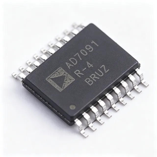
The AD7091R-2BRUZ from Analog Devices is a 12-bit successive approximation register (SAR) analog-to-digital converter (ADC) that operates from a single 2.7V to 5.25V power supply and achieves a sampling rate of 1 MSPS. It features two single-ended analog input channels, an on-chip 2.5V reference, and a high-speed serial interface (SPI). The device is housed in a 16-lead TSSOP package, making it suitable for space-constrained applications. A SAR ADC is a type of analog-to-digital converter that uses a binary search algorithm to convert an analog input into a digital output. It is known for its high speed, low power consumption, and ease of use, making it ideal for applications such as data acquisition, industrial control, and portable instrumentation. The AD7091R-2 is part of the AD7091R family, which includes 2-, 4-, and 8-channel versions, all sharing the same core architecture and performance characteristics. Key features of the AD7091R-2BRUZ include ultralow power consumption (typically 367 µA at 3V and 1 MSPS), a wide bandwidth track-and-hold amplifier that can handle input frequencies in excess of 1.5 MHz, and an on-chip conversion clock that simplifies system design. The device also includes a channel sequencer that allows preprogrammed selection of channels to be converted sequentially, enhancing flexibility in multi-channel applications. The AD7091R-2BRUZ uses a SAR architecture with an internal reference and a high-speed serial interface that supports data read after conversion, achieving a 1 MSPS throughput rate with a 50 MHz SCLK. The device is designed for low power and high accuracy, with a typical power dissipation of less than 2 mW at 3V, making it suitable for battery-powered and portable applications. Typical applications include battery monitoring, data acquisition systems, industrial process control, and portable instrumentation. The wide input bandwidth and low power consumption make it ideal for applications requiring high-speed, low-power analog-to-digital conversion. When designing with this device, ensure that the analog input voltage does not exceed the supply voltage and that adequate decoupling capacitors are placed near the power supply pins. The SPI interface should be configured for the correct clock polarity and phase to ensure reliable data transfer.

RFQ رابطہ
AD7091R-4BRUZ - 4-Ch 12-Bit 1MSPS SAR ADC | Analog Devices
AD7091R-4BRUZ

AD7091R-4BRUZ - 4-Ch 12-Bit 1MSPS SAR ADC | Analog Devices

The AD7091R-4BRUZ is a 4-channel, 12-bit, ultralow power, successive approximation (SAR) analog-to-digital converter (ADC) from Analog Devices. It operates from a single 2.7 V to 5.25 V power supply and achieves a sampling rate of 1 MSPS. The device features an on-chip 2.5 V reference, an on-chip conversion clock, and a high-speed SPI-compatible serial interface. It is available in a 20-lead TSSOP package, making it suitable for space-constrained applications. An ADC (analog-to-digital converter) is a device that converts continuous analog signals into discrete digital numbers. The AD7091R-4BRUZ is a SAR ADC, which uses a binary search algorithm to determine the digital output. SAR ADCs are known for their high speed, low power, and ease of use, making them ideal for a wide range of applications. The AD7091R-4BRUZ is part of the AD7091R family, which includes 2-, 4-, and 8-channel versions, all sharing the same core architecture. Key features of the AD7091R-4BRUZ include ultralow power consumption: normal mode draws only 1.4 mW at 1 MSPS, and power-down mode draws 550 nA typical at VDD = 5.25 V and 435 nA at VDD = 3 V. The device also features a programmable ALERT interrupt pin (on 4- and 8-channel models) for monitoring out-of-range conditions. The on-chip 2.5 V reference eliminates the need for an external reference, simplifying design. The AD7091R-4BRUZ uses a flexible power/throughput rate management scheme, allowing the conversion rate to be adjusted to match the system's needs, thereby optimizing power consumption. The SPI interface supports data read after conversion, achieving a 1 MSPS throughput rate. The device also includes a channel sequencer that allows preprogrammed selection of channels to be converted sequentially, reducing microcontroller overhead. Typical applications include battery-powered instrumentation, portable medical devices, industrial process control, and data acquisition systems. The low power consumption and small package make it ideal for portable and battery-operated equipment. When designing with the AD7091R-4BRUZ, ensure that the analog input voltage does not exceed the supply voltage to avoid damage. Use a low-pass filter on the analog inputs to reduce noise and aliasing. The reference voltage is internally generated, but an external reference can be used if higher accuracy is required.

USD $3.04 رابطہ