انٹرفیس ICs
ذیلی زمرے
مصنوعات (320+)

FUSB302MPX - USB Type-C Controller with PD | onsemi
The onsemi FUSB302MPX is a programmable USB Type-C controller with Power Delivery (PD) support, operating from a 2.8V to 5.5V supply and packaged in a 14-pin MLP (2.5x2.5 mm) package with exposed pad. It is a USB 3.1 companion USB interface IC designed to implement the USB Type-C connection management and Power Delivery protocol layers. A USB Type-C controller is a dedicated interface IC that manages the CC (Configuration Channel) lines of a USB Type-C connector. In the system hierarchy, it sits between the USB power path / USB 3.1 physical connector and the host microcontroller, handling attach detection, cable orientation, role swap, and PD message negotiation so the application processor does not need to bit-bang the PD protocol. Key features of the FUSB302MPX include full USB Type-C CC-line termination and detection, a full-featured PD PHY supporting BMC (Biphase Mark Coding) signaling on the CC line, an I2C slave interface for host control, and integrated VCONN support for powering electronically marked cables. The programmable architecture lets firmware implement sink, source, or dual-role power policies in software. Technically, the device integrates a PD transceiver with BMC encoding/decoding, comparator-based CC voltage monitoring for attach and orientation detection, and register-based configuration accessible over I2C at up to 400 kHz clock rates. The exposed-pad MLP-14 package provides low thermal impedance and short trace lengths, which benefits CC-line signal integrity at BMC data rates. RoHS-compliant, lead-free construction supports modern environmental requirements. Typical applications include USB Type-C power adapters and chargers, smartphone and tablet port controllers, notebook and dock power negotiation, power banks with PD sink input, and monitor or display-port alternate-mode designs. In each case the FUSB302MPX handles CC attach detection and PD contract negotiation while the system MCU manages the actual power conversion stage. A key design consideration: onsemi explicitly recommends the FUSB302BMPX for new designs; the FUSB302B family incorporates updates aligned to later USB-C specification releases, and per onsemi the B version is a drop-in replacement requiring no software optimization. This page adds value beyond the manufacturer datasheet by synthesizing distributor availability, drop-in alternative guidance, design notes, and comparison data in one engineer-oriented reference.
FUSB303TMX - USB Type-C Port Controller I2C 15W | onsemi
The onsemi FUSB303TMX is a fully autonomous USB Type-C port controller with I2C and GPIO control, optimized for 15 W or less applications, housed in a 12-terminal X2QFN (1.6 x 1.6 mm) package. A USB Type-C port controller (also called a Type-C port controller, TCPC, or CC logic IC) manages the Configuration Channel (CC) lines of a USB-C connector. It detects cable attach and detach, determines source/sink role, handles DRP (Dual-Role Port) toggling, and supports accessory and audio/headphone adapter detection. Within the power-management and interface hierarchy of a USB-C system, the port controller sits between the CC pins of the connector and the system host controller (MCU, PMIC, or SoC), offloading connection-state management so the host need not constantly poll the CC lines. Key features include fully autonomous CC logic detection for Source, Sink, DRP, and accessory roles, Dead Battery support as defined by USB-C specifications, and a configurable I2C slave address that allows multiple ports per system to share one I2C bus. GPIO control offers an additional mode for systems without an I2C host. The tiny 1.6 x 1.6 mm 12-X2QFN footprint minimizes PCB area in space-constrained designs. Architecturally, the FUSB303 integrates the CC line comparators, Rp/Rd switches, and state machine needed for autonomous operation, requiring minimal host intervention once configured over I2C. This reduces firmware complexity and lowers overall system power compared with host-managed CC detection schemes. Typical applications include smartphones, tablets, and other battery-powered consumer devices with 15 W or lower USB-C charging; power banks and dock accessories requiring role detection; and embedded systems adding USB-C connectivity where Dead Battery support is mandatory. Design consideration: verify the I2C address configuration of each FUSB303 instance on a shared bus and ensure CC-line routing to the connector is short and matched to maintain detection robustness. This page synthesizes distributor pricing, drop-in alternatives, and practical design notes not found in the manufacturer datasheet.
FUSB340TMX - USB 3.1 10 Gbps 2:1 Data Switch | onsemi
The onsemi FUSB340TMX is a USB 3.1 SuperSpeed 2:1 data switch supporting 5 Gbps and 10 Gbps data rates, housed in an 18-pin TMLP (2x2.8 mm) package. Targeted at the mobile device market, it routes SuperSpeed differential pairs between a USB Type-C receptacle and either an upstream hub or sideband connection, enabling reversible-cable topologies without an extra mux. The device operates across USB SuperSpeed Gen1 (5 Gbps), Gen2 (10 Gbps), PCIe Gen3, SATA, DisplayPort 1.3, and Fibre Channel protocols, making it suitable as a generic 10 Gbps differential switch. A USB 3.1 data switch is a high-speed analog multiplexer that routes SuperSpeed differential pairs (TX/RX) between two physical paths while preserving signal integrity at multi-gigahertz frequencies. As a Type-C accessory switch, it is one of several functional blocks in a USB Type-C implementation: Type-C controller -> high-speed data switch -> SBU/AUX switch -> USB-PD controller. The FUSB340TMX specifically occupies the high-speed data mux role, enabling USB-C reversible-cable operation in phones, tablets, and laptops. Key features include 10 Gbps SuperSpeed Gen2 support, 2:1 switch topology, low insertion loss and return loss over the SuperSpeed frequency range, channel-to-channel skew designed for USB 3.1 compliance, and an operating range suitable for portable and battery-powered designs. The compact 2x2.8 mm TMLP package and minimal external component count simplify PCB layout in space-constrained mobile designs. The FUSB340 uses an adaptive signal-path topology that maintains 50-ohm characteristic impedance in both the active and idle states to minimize reflections. The wide -3 dB bandwidth accommodates PCIe Gen3 (8 Gbps) and DisplayPort 1.3 (8.1 Gbps) RBR/HBR signalling with margin, making the part usable as a generic high-speed differential mux beyond strict USB roles. Typical applications include USB Type-C reversible-cable multiplexers, mobile phone and tablet accessory switches, USB 3.1 Gen2 hub fan-out, notebook sideband routing, and Thunderbolt 3 alternate-mode signal multiplexing. The part is also used in docking stations that share USB SuperSpeed lines between multiple hosts. When designing with the FUSB340TMX, keep the SuperSpeed differential traces length-matched to within 150 mils and route them over a continuous ground reference. Place the decoupling capacitor within 2 mm of the supply pin, and avoid routing any digital control lines directly under the high-speed traces to prevent crosstalk. This page synthesizes distributor pricing, drop-in alternative parts from the same TI and Microchip ecosystems, and practical layout notes that are not present in the manufacturer datasheet.

FXL6408UMX - 8-Bit I2C GPIO Expander 400kHz 16-UMLP | onsemi
The onsemi FXL6408UMX is a fully configurable 8-bit I2C-controlled GPIO expander with a 400 kHz I2C interface, an operating supply range of 1.65 V to 4 V, and a compact 16-pin UMLP package measuring 1.8 x 2.6 mm. It expands a host processor's I/O capability over the industry-standard two-wire I2C serial bus while supporting bidirectional voltage translation between the I2C bus domain and the GPIO pin domain. A GPIO (General Purpose Input/Output) expander is a type of interface IC in the logic family hierarchy that adds digital input and output pins to a microcontroller or baseband processor through a serial bus. Where the host MCU or SoC lacks enough parallel I/O pins, an I2C GPIO expander converts two bus pins (SDA and SCL) into eight additional configurable I/O lines, making it a core building block of system I/O management and power-management-adjacent designs. Key features include input transition monitoring with an interrupt output: when configured in Input Mode, the FXL6408 watches the input ports for data transitions and asserts the /INT pin to signal the baseband or host. Default input values can be programmed independently, allowing customized input detection thresholds. All eight inputs can be configured with internal pull-up or pull-down resistors, pre-biasing the inputs for open-drain or push-pull operation without external components. Technically, the device implements a register-based configuration model in which each pin's direction, polarity, pull resistor, and default state are set through I2C write cycles at up to 400 kHz (Fast-mode). The wide 1.65 V to 4.0 V supply range lets one part interface between low-voltage (1.8 V) processors and legacy 3.3 V peripherals, and the small-footprint UMLP-16 package suits space-constrained portable designs. Typical applications include smartphone and tablet baseband I/O expansion, keyboard and button matrices, LED and backlight status indication, and sensor or peripheral status monitoring in portable and industrial systems where the host MCU lacks spare GPIO. Design consideration: keep the I2C bus within 400 kHz Fast-mode timing and use the programmable pull resistors to avoid external resistor networks; account for the /INT open-drain output requiring a pull-up to the host logic rail. This page synthesizes distributor pricing, drop-in alternatives, and practical design notes not found in the manufacturer datasheet.

GL850G-HHY22 - USB 2.0 4-Port Hub Controller | Genesys Logic
The Genesys Logic GL850G-HHY22 is a USB 2.0 hi-speed hub controller supporting up to 4 downstream ports, 480 Mbps signaling, and 0C to +85C operation, housed in a 28-pin SSOP (SSOP-28) package. It operates from dual supply rails of 4.75V to 5.25V and 3V to 3.6V. A USB 2.0 hub controller is an interface IC that sits between a USB host and one or more downstream USB devices, repeating and managing traffic according to the Universal Serial Bus Specification Revision 2.0. Hub controllers fall within the broader hierarchy of USB interface controllers, peripheral ICs, and semiconductors, and are fundamental building blocks in any system that needs to expand a single USB port into several. The GL850G embeds an 8-bit RISC processor that manages control and status registers and responds directly to requests from the USB host, offloading hub transaction translation from the host CPU. It is Genesys Logic's advanced, cost-optimized hub solution and complies fully with USB Specification Revision 2.0, supporting low-speed (1.5 Mbps), full-speed (12 Mbps), and hi-speed (480 Mbps) devices. Power management supports both Individual and Gang modes across the four downstream ports, with two-color (green/amber) port status indication for LED-based port state feedback. Architecturally, the GL850G inherits Genesys Logic's cost- and power-efficient serial interface design, delivering proven compatibility and a low-power profile compared with competing hub solutions. Its integrated RISC core and minimal external component count help system integrators achieve the lowest possible BOM (Bill of Materials) for motherboards, monitors, docking stations, and standalone USB hubs. Typical applications include standalone multi-port USB hubs, PC motherboard front-panel and rear-panel USB port expansion, monitor and display USB uplink ports, embedded systems, and industrial equipment requiring reliable USB 2.0 port multiplication. For systems requiring higher full/low-speed performance with multiple transaction translators, Genesys Logic offers the GL852G multi-TT hub family. Design considerations: provide clean 3.3V and 5V rails within the specified 4.75V to 5.25V and 3V to 3.6V windows, and observe the 0C to +85C commercial operating range. Proper crystal or oscillator placement and USB differential pair routing (90-ohm matched) are essential for passing USB-IF signal integrity compliance. This page synthesizes distributor pricing (as of 2026-10-19), stock data, family alternatives, and practical design notes not found in the manufacturer datasheet alone.
GX36220-DNT - 2x64Gb/s Linear TIA Die | Renesas | 400G Coherent
The Renesas Electronics GX36220-DNT is a dual 32Gb/s (2x64Gb/s aggregate) linear transimpedance amplifier (TIA) supplied in bare-die form under the DIE SALE (PRICE IN GOOD DIE) wafer program. The GX36220 integrates two independent TIA signal paths for the I and Q channels of 400G coherent Receiver Optical Sub-Assemblies (ROSAs), delivering the linear gain transfer behavior required by modern coherent DSP-based optical receivers. A transimpedance amplifier is a type of current-to-voltage converter that sits directly behind a photodiode in an optical receiver, converting the photodiode's weak photocurrent into a usable differential voltage while adding minimal noise. Within the optical signal chain hierarchy, the TIA is the first gain stage after the photodetector and directly determines receiver sensitivity, overload behavior, and linearity - the latter being essential for coherent systems that rely on DSP equalization rather than hard limiting. Key characteristics include dual-channel integration (I and Q), a 32Gb/s per-channel data rate, and linear (non-limiting) output operation, which preserves signal amplitude information for the downstream coherent DSP. Linear TIAs are critical in coherent optical transceivers where limiting amplifiers would destroy the phase and amplitude modulation content of the received signal. The DNT suffix identifies the die-sale ordering option: parts are sold as known-good die from wafer processing, allowing integration into hermetically sealed or hybrid optical sub-assembly packages, butterfly packages, or custom ROSA modules. This delivery format minimizes package parasitics and supports the compact form factors demanded by 400G and beyond coherent transceiver designs. Typical applications include 400G coherent ROSA I/Q channel amplification, coherent DWDM receiver front ends, telecom datacenter-interconnect optical receivers, and hybrid photonic integrated receiver assemblies. Each 32Gb/s channel handles one quadrature of the coherent signal, so a single GX36220 supports a complete dual-quadrature receiver front end. Design consideration: because this part is supplied as bare die, assembly requires die-attach and wire-bond or flip-chip processes with controlled bond-length inductance; pinout and die mechanical drawings must be taken from the manufacturer datasheet and die-spec documentation before hybrid layout begins. This page synthesizes distributor pricing, availability, die-ordering details, and practical design notes not found in the manufacturer datasheet.
GX76476-DNT - 4x64Gbaud Linear Driver | Renesas Electronics
The Renesas Electronics GX76476-DNT is a low-power, high-performance quad-channel linear differential I/O driver designed for 64 Gbaud per lane operation (4 x 64 Gbaud aggregate) in 400G/600G optical integrated transmitter small form factor (SFF) modules for metro and long-haul applications. Each of the four integrated driver lanes provides a 100 ohm differential AC-coupled input and a 60 ohm output, with on-chip SPI circuitry for DC controls, all integrated on a single die. A linear driver is an analog interface IC that amplifies the modulator drive signal without slicing or retiming, preserving the analog waveform so the optical modulator (typically a silicon photonics Mach-Zehnder or electro-absorption modulator) can produce multi-level signals such as PAM4. Linear drivers sit in the signal chain hierarchy between the DSP serdes output and the modulator, and together with a linear transimpedance amplifier (TIA) on the receive side they form the analog front end of a coherent or PAM4 optical transmission link. Key features of the GX76476 include quad-lane integration that reduces BOM count and footprint versus discrete single-lane drivers, linear (non-limiting) operation enabling multi-level modulation formats, low power consumption per channel, and SPI-programmable DC control parameters for per-channel output amplitude and bias optimization. The 64 Gbaud lane rate supports both 400G (4 x 100G PAM4) and 600G module configurations used in data-center interconnect and telecom metro/long-haul links. Technically, the device integrates four matched driver lanes plus SPI control circuitry on one die, giving excellent channel-to-channel skew and gain matching - critical for PAM4 eye symmetry at 64 Gbaud. The 100 ohm differential AC-coupled input matches the standard serdes output impedance, while the 60 ohm output is designed for the load impedance typical of driving arrangements in integrated coherent transmit (ICT) and integrated transmit subassembly (ITMA) optical architectures. Typical applications include 400G and 600G optical transmitter SFF modules, metro and long-haul coherent optical transceivers, data-center interconnect (DCI) line cards, and pluggable or embedded optical modules using silicon photonics transmitters. A key design consideration is thermal management: four high-speed driver lanes concentrated on a single die dissipate significant heat, so the host module must provide an adequate thermal path from the die/paddle, and SPI-based bias tuning should be performed after thermal characterization. This page synthesizes verified distributor pricing, cross-reference results, and design guidance beyond what the short-form manufacturer datasheet alone provides.

ISD8104RYI - 2W Class AB Audio Amplifier | Nuvoton
The Nuvoton ISD8104RYI is a 2W mono Class AB audio power amplifier IC with differential input pair and chip enable, manufactured by Nuvoton Technology Corporation. The RYI suffix denotes the SOP-8 surface-mount package with exposed thermal pad option family, and the device integrates a single-channel (mono) amplifier output stage in a compact 8-pin footprint. A Class AB audio amplifier is a linear power amplifier topology in which output transistors conduct continuously through the signal cycle, combining the low distortion of Class A designs with the improved efficiency of Class B. Within the power management and audio signal chain hierarchy, it sits downstream of DACs or codec outputs and upstream of the loudspeaker, converting line-level analog signals into speaker-drive-capable power. The ISD8104 belongs to Nuvoton's ISD audio amplifier product line, alongside the ISD8102, which differs by offering an earphone-sense input (SE/Diff) instead of a dedicated differential input pair. Key features include 2W output power at mono Class AB operation, a true differential input pair that rejects common-mode noise picked up on the PCB, and a chip enable (CE) pin that allows the system controller to shut the amplifier down and minimize standby current draw in battery-powered products. The differential input architecture is significant for designs where the amplifier sits far from the signal source, such as alarm panels or appliance panels. The Class AB output stage provides low crossover distortion, important for voice-band announcement and alerting audio where intelligibility matters more than maximum efficiency. Typical applications include doorbell and intercom systems, industrial alarm sounders, small appliance voice prompts, toys, and battery-powered notification devices. When designing with the ISD8104RYI, consult the manufacturer datasheet for gain-setting resistor values, supply voltage limits, and the thermal pad soldering requirements, since power dissipation in a 2W Class AB stage depends strongly on supply voltage and load impedance. This page synthesizes distributor listings, same-family drop-in alternatives, and practical design notes not found in the manufacturer datasheet alone.

ISD9361RI - Serial Voice Record/Playback IC, 64-LQFP | Nuvoton
The Nuvoton Technology ISD9361RI is a serial-interface voice record and playback IC (Message Serial series) supplied in a 64-pin LQFP package measuring 7 x 7 mm, rated for an operating temperature range of -40C to +85C. The device integrates the analog audio front end and message management logic required to record and play back voice messages under serial control from a host microcontroller. A voice record and playback IC is a mixed-signal audio device that converts microphone input into stored digital audio and converts stored digital data back into analog sound using an integrated codec, speaker driver interface, and message indexing engine. Such devices sit within the broader hierarchy of audio codec ICs and human-machine-interface semiconductors, where they offload audio capture and playback tasks from the main processor. Key features of the ISD9361RI include its serial host interface, message-based storage architecture for indexed voice segments, integrated record and playback paths, industrial-grade temperature rating from -40C to +85C, and a compact 7 x 7 mm 64-LQFP surface-mount package that suits dense PCB layouts. The message-serial architecture allows a host controller to address individual voice messages, enabling prompt-driven user interfaces without streaming raw audio data over the bus. Technically, the device combines an analog front end for microphone and line inputs with a digital message-management core, providing self-contained record/playback sequencing. Host controllers issue serial commands to trigger specific messages, simplifying firmware in applications that only need canned announcements or prompt playback. Typical applications include industrial equipment voice annunciators, medical device audible prompts, security and alarm announcement panels, elevator and building-automation voice prompts, and consumer appliance user interfaces. Design consideration: because the ISD9361RI is officially listed as obsolete, new designs should secure long-term stock or plan a successor strategy before committing to this part; verify message storage duration and audio bandwidth against the manufacturer datasheet. This page synthesizes distributor stock data, lifecycle status, and sourcing guidance for an obsolete Nuvoton voice IC - information not consolidated in the manufacturer datasheet.

ISL33001IUZ - I2C Bus Buffer, Hot-Swap 2-Ch | Renesas
The Renesas Electronics ISL33001IUZ is a 2-channel I2C bus buffer with rise-time accelerators and hot-swap capability, extending I2C bus capacitance beyond the 400 pF limit specified by the I2C specification, supplied in an 8-pin MSOP (IUZ) package rated for the industrial -40C to +85C temperature range. An I2C bus buffer (also called a bus repeater or signal buffer) is an interface IC that sits between an I2C controller segment and a heavily loaded peripheral segment. The I2C specification limits total bus capacitance to 400 pF, which restricts the number of devices, trace length, and pull-up resistance a system can support. A bus buffer regenerates the SDA and SCL edges, segmenting the bus so each side only sees its own local capacitance, allowing much larger backplanes, card cages, and cable runs. Key features of the ISL33001 include two independent buffered channels (SDA and SCL), rise-time accelerator circuitry that drives rising edges actively to reduce power dissipated in passive pull-up resistors and enable faster data rates, and integrated hot-swap circuitry that prevents SDA/SCL corruption when a board is inserted into or removed from a live backplane. The device supports standard and fast-mode I2C operation with level-tolerant I/O structure. Architecturally, the buffer uses a dual-direction translator between the controller-side and card-side pins: a low level on either side propagates to the other, while levels are re-driven with controlled rise times. This bidirectional, transparent behavior requires no mode control in typical single-controller systems. The hot-swap input stage holds the local bus pins low or high-impedance during power ramp until VCC stabilizes, avoiding spurious start or stop conditions during card insertion. Typical applications include server and telecom backplanes, I2C fan controllers, optical-module management (SFP/QSFP style management buses), battery-management and hot-pluggable card rails, and long cable runs between chassis in industrial systems. Design consideration: rise-time accelerators pull up only during edges; ensure adequate static pull-up resistance on the far side of the buffer for DC low-level sinks, and keep the EN/enable pin controlled during power sequencing to avoid bus glitches. This page synthesizes distributor pricing, drop-in family alternatives (ISL33002/ISL33003), and practical design notes not found in the manufacturer datasheet.
ISL33002IUZ-T - 2-Ch I2C Bus Buffer Hot-Swap | Renesas
The Renesas Electronics ISL33002IUZ-T is a two-channel bidirectional I2C bus buffer with rise-time accelerators and hot-swap capability, operating from a +2.3V to +5.5V supply at over 400kHz, housed in an 8-lead MSOP package. An I2C bus buffer, also called a bus accelerator or signal repeater, is an interface IC that regenerates the SDA and SCL signals so the total bus capacitance can exceed the 400pF limit defined by the I2C specification. Within the signal-chain hierarchy (buffer -> interface IC -> signal buffer/repeater), bus buffers isolate capacitance on either side of the device, allowing long cables, large backplanes, and high fan-out systems to communicate reliably at standard I2C data rates. Key features include bus capacitance buffering beyond the 400pF I2C maximum, rise-time accelerator circuitry that reduces power consumption otherwise wasted in passive pull-up resistors while improving data-rate performance, hot-swap circuitry that prevents bus corruption during live card insertion, and robust ESD protection of ±6kV Class 3 HBM on all pins, with ±12kV HBM on the SDA/SCL pins. The device supports logic level translation between voltage domains, includes an accelerator disable pin for flexible system control, and provides low quiescent current. Operation over an industrial -40C to +85C temperature range makes the -T (tape-and-reel, industrial temperature grade) variant suitable for factory and telecom equipment. The 8 Ld MSOP occupies only 3mm x 3mm of board area. Typical applications include I2C bus extension across backplanes and racks, hot-swappable line cards, level translation between 1.8V/3.3V/5V domains, and server or networking chassis management buses (such as IPMB-style monitoring). The buffer fits wherever capacitance, cable length, or card insertion would otherwise corrupt I2C signaling. A key design consideration: enable the accelerator circuit only when bus rise times are marginal with the chosen pull-up resistors, since excessive acceleration can cause signal ringing on lightly loaded buses. This page synthesizes distributor pricing, drop-in alternatives, and practical design notes not found in the manufacturer datasheet.
ISL33003IUZ-T - I2C Bus Buffer, Hot-Swap, 8-MSOP | Renesas
The Renesas Electronics ISL33003IUZ-T is a two-channel I2C bus buffer with rise-time accelerators and hot-swap capability, supplied in an 8-MSOP surface-mount package for industrial -40C to +85C operation. An I2C bus buffer (also called a bus repeater or signal buffer) is an interface IC that regenerates the two-wire SDA and SCL signals of an I2C bus, extending the total bus capacitance beyond the 400 pF limit specified by the I2C specification. Within the interface IC hierarchy (bus buffer -> signal buffer/repeater -> interface IC -> semiconductor), buffers let designers add more devices, longer cables, and larger PCB traces to an I2C segment without sacrificing signal integrity or data-rate performance. Key features of the ISL33003 include capacitance extension beyond the 400 pF I2C limit, rise-time accelerator circuitry that reduces the power consumed by passive pull-up resistors while improving data-rate performance, and hot-swap circuitry that prevents corruption of the bus during card insertion or removal. The two channels allow buffering of both SDA and SCL in one compact 8-MSOP package. Technically, the buffer separates capacitive loading on either side of the device, isolating a heavily loaded segment from the controller segment. The rise-time accelerators actively pull the bus lines high during transitions, allowing weaker (higher-value, lower-power) pull-up resistors to be used without slowing edge rates. The hot-swap function keeps the I/O pins high-impedance until the local supply stabilizes, avoiding bus latch-up or data corruption during live insertion. Typical applications include backplane and card-cage systems with pluggable I2C cards, server and telecom chassis management (I2C/PMBus sensor rails), and long bus runs in industrial control where many EEPROMs, RTCs, or I/O expanders share one bus. Design consideration: place the buffer physically between the capacitive segments, and follow the datasheet recommendations for pull-up sizing and accelerator enable configuration to avoid false START conditions. This page synthesizes distributor pricing, drop-in family alternatives, and practical design notes not found in the manufacturer datasheet alone.

ISO1042 - Isolated CAN Transceiver with 70V Fault Protection | TI
The Texas Instruments ISO1042 is a galvanically-isolated controller area network (CAN) transceiver that meets the specifications of the ISO11898-2 (2016) standard. It offers ±70V DC bus fault protection and ±30V common-mode voltage range, making it robust for industrial and automotive networking. The device supports data rates up to 5 Mbps in CAN FD mode, enabling faster payload transfer compared to classic CAN. It is available in an 8-pin SOIC (DW) package and operates over a wide temperature range. A CAN transceiver is a physical-layer device that interfaces between the CAN protocol controller and the differential bus lines. It converts the digital signals from the controller into differential signals for transmission and vice versa. The ISO1042 adds galvanic isolation, which separates the bus side from the logic side, preventing ground loops and protecting low-voltage electronics from high-voltage transients. This isolation is critical in industrial environments where long bus lines and potential ground potential differences exist. Key features include reinforced isolation with a working voltage of 1000 Vrms, a common-mode voltage range of ±30V, and bus fault protection up to ±70V. The device also features a silent mode for bus monitoring and a dominant timeout function to prevent bus lock-up. Its low loop delay of 150 ns ensures high-speed communication, and it is compliant with ISO11898-2 (2016) and ISO11898-5 standards. The ISO1042 uses TI's capacitive isolation technology, which provides high immunity to magnetic interference and supports high data rates. The isolation barrier is rated for 5000 Vrms surge, ensuring reliable operation in harsh environments. The device is designed for use in automotive and industrial applications, including electric vehicles, battery management systems, and factory automation. Typical applications include automotive body control modules, industrial fieldbus networks, and building automation. The ISO1042 is also suitable for solar inverters and motor drives where galvanic isolation is required for safety. Its robust fault protection and high common-mode range make it ideal for long bus lines in noisy environments. When designing with the ISO1042, ensure proper PCB layout with adequate creepage and clearance distances for the isolation barrier. Use a 100 nF bypass capacitor on the VCC pin and a 10 µF capacitor on the VIO pin for stable operation. The device requires a single 3.3V or 5V supply on the logic side and a 5V supply on the bus side.
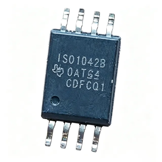
ISO1042BDWVR - Isolated CAN FD Transceiver 5Mbps 70V | TI
The Texas Instruments ISO1042BDWVR is a galvanically-isolated CAN transceiver supporting flexible data rates up to 5 Mbps (CAN FD capable), with 70-V bus fault protection and a working isolation voltage of 1060 Vrms, housed in an 8-pin wide-body SOIC (DWV) package rated from -40C to +125C. A CAN transceiver is the physical-layer interface device that translates logic-level signals from a CAN controller into differential bus signals (CANH/CANL) and back. Within the system hierarchy it sits between the protocol controller and the twisted-pair bus, and isolated variants like the ISO1042 belong to the broader class of digital-isolator-based interface ICs used in industrial and automotive networks. Key features include 70-V bus fault protection (far beyond the -27V to 40V tolerance of typical transceivers), a 5 Mbps flexible data rate for CAN FD frames, and logic-side supply flexibility from 1.8V to 5.5V, allowing direct connection to low-voltage microcontrollers without level shifting. Integrated bus-pin ESD protection of +/-16 kV HBM, thermal shutdown, and dominant-timeout functions further harden the interface. Architecturally, the device integrates the TX and RX signal isolation channels across TI's capacitive isolation barrier plus the CAN bus driver/receiver in one package, eliminating a separate digital isolator in front of a standard transceiver. The low loop delay of 152 ns supports longer bus lengths and faster arbitration in CAN FD communication, and the device meets ISO11898-2 (2016) standard specifications. Typical applications include industrial automation and motor drive networks, building automation, NVIDIA Jetson-style embedded compute platforms requiring a CAN FD isolator, automotive body electronics (the ISO1042BQDWVRQ1 variant), and medical equipment needing safety isolation between controller and bus. For design, maintain creepage and clearance around the isolation barrier in PCB layout, supply the logic side at 1.8V or 5.5V as specified, and place the 120-ohm bus termination per standard CAN practice. This page synthesizes distributor pricing, drop-in alternatives, and practical design notes not found in the manufacturer datasheet. Pricing at authorized distributors starts near $0.77 as of 2026-09-01.
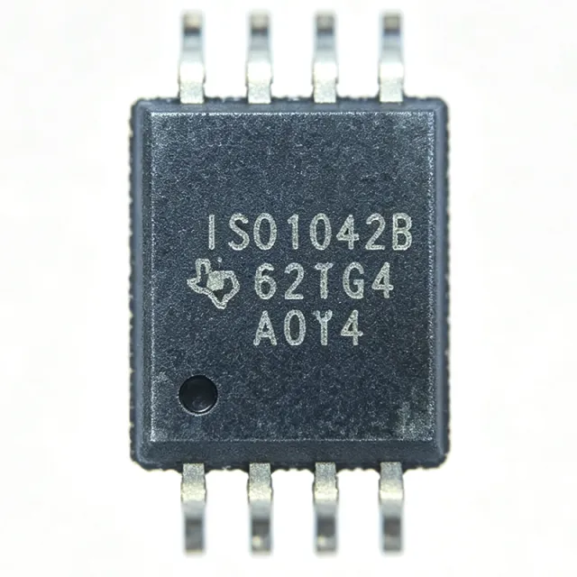
ISO1042BQDWVRQ1 - 5Mbps Isolated CAN FD Transceiver | TI
The Texas Instruments ISO1042BQDWVRQ1 is an AEC-Q100 qualified, galvanically-isolated CAN FD transceiver supporting data rates up to 5 Mbps, with ±70-V DC bus fault protection and a ±30-V common-mode voltage range, housed in an 8-pin wide-body SOIC (DWV) package. An isolated CAN transceiver is a signal interface IC that combines a CAN physical-layer transceiver with a digital isolator in a single package. In the system hierarchy, it sits between the host microcontroller or CAN controller (logic side) and the two-wire CAN bus (bus side), providing galvanic isolation that blocks ground loops, common-mode transients, and high-voltage faults - critical in vehicles and industrial networks where nodes span large distances and different ground domains. Key features include support for CAN FD flexible data rates up to 5 Mbps, enabling much faster payload transfer than classic CAN's 500 kbps; a logic-side supply range down to 1.8 V for direct interfacing with low-voltage MCUs; and robust protection with ±70-V DC bus fault tolerance. The device meets the ISO11898-2 (2016) standard and integrates one driver and one receiver channel with typical operating supply current of about 43 mA. The ISO1042-Q1 family uses TI capacitive isolation technology, providing a reliable galvanic barrier suited to automotive and industrial environments. The wide-body SOIC-8 (DWV) package provides substantial creepage and clearance distance across the isolation barrier, supporting basic and reinforced isolation ratings. Typical applications include electric vehicle powertrain and battery management networks, body control modules, industrial PLC and motor drive CAN buses, and building automation nodes - anywhere CAN nodes must be isolated from ground potential differences or bus faults. Design consideration: use split-termination or 120-ohm bus termination per ISO11898-2, and place 100-nF decoupling capacitors close to both VCC1 and VCC2 pins to maintain signal integrity at 5-Mbps CAN FD bit rates. This page synthesizes distributor pricing, drop-in alternatives, comparison data, and practical design notes not found in the manufacturer datasheet alone.
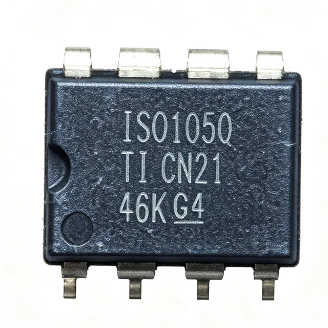
ISO1050DUB - Isolated CAN Transceiver 2500Vrms | TI (Tape & Reel)
The Texas Instruments ISO1050DUB is a galvanically isolated CAN transceiver that meets or exceeds the specifications of the ISO 11898-2 standard, delivering 1 Mbps half-duplex CAN communication with 2500 Vrms silicon oxide (SiO2) isolation in an 8-pin SOP (DUB) package. An isolated CAN transceiver combines a CAN protocol controller interface with galvanic isolation, allowing data transmission between nodes without a direct electrical connection. Within the signal chain hierarchy, it sits between the CAN controller and the physical twisted-pair bus, isolating the logic domain from the bus domain. Isolation prevents ground loops, common-mode noise, and voltage spikes from damaging sensitive controller electronics in industrially noisy environments. Key features include a SiO2 insulation barrier rated 2500 Vrms for the DUB package (the ISO1050DW variant reaches 5000 Vrms), failsafe outputs, low loop delay of 150 ns typical, and 50 kV/us typical transient immunity. Bus-fault protection extends to -40V on the bus pins, and the device operates from -55C to +105C. Both logic and bus sides operate from a 5V supply. Architecturally, the ISO1050 uses an on-chip capacitive SiO2 isolation barrier providing high-speed signal transfer with low power consumption. The transceiver drives CANH and CANL differentially, supports dominant/recessive bus states per ISO 11898-2, and includes thermal shutdown protection on the bus driver. Typical applications include industrial automation networks such as CANopen and DeviceNet, motor drives, building automation, battery management systems, and EV charging stations where ground potential differences exist between nodes. Design tip: use a dedicated isolated DC-DC supply for the bus side and maintain adequate creepage and clearance on the PCB around the barrier. For higher isolation (5000 Vrms), select the ISO1050DW; TI recommends the ISO1042 or ISO1044 as successors for new designs. This page synthesizes distributor pricing, drop-in alternative cross-references, and practical design notes not found in the manufacturer datasheet. Pricing as of 2026-09-01 from LCSC listing data.
ISO1050DUBR - Isolated CAN Transceiver 2500Vrms | TI
The Texas Instruments ISO1050DUBR is a galvanically isolated CAN transceiver that meets or exceeds the specifications of the ISO 11898-2 standard, delivering 1 Mbps half-duplex CAN communication with 2500 Vrms silicon oxide (SiO2) isolation in an 8-pin SOP (DUB) package. An isolated CAN transceiver combines a CAN protocol controller interface with galvanic isolation, allowing data transmission between nodes without a direct electrical connection. Within the signal chain hierarchy, it sits between the CAN controller and the physical twisted-pair bus, isolating the logic domain from the bus domain. Isolation prevents ground loops, common-mode noise, and voltage spikes from damaging sensitive controller electronics in industrially noisy environments. Key features include a SiO2 insulation barrier rated 2500 Vrms for the DUB package (the ISO1050DW variant reaches 5000 Vrms), failsafe outputs, low loop delay of 150 ns typical, and 50 kV/us typical transient immunity. Bus-fault protection extends to -40V on the bus pins, and the device operates from -55C to +105C. Both logic and bus sides operate from a 5V supply. Architecturally, the ISO1050 uses an on-chip capacitive SiO2 isolation barrier providing high-speed signal transfer with low power consumption. The transceiver drives CANH and CANL differentially, supports dominant/recessive bus states per ISO 11898-2, and includes thermal shutdown protection on the bus driver. Typical applications include industrial automation networks such as CANopen and DeviceNet, motor drives, building automation, battery management systems, and EV charging stations where ground potential differences exist between nodes. Design tip: use a dedicated isolated DC-DC supply for the bus side and maintain adequate creepage and clearance on the PCB around the barrier. For higher isolation (5000 Vrms), select the ISO1050DW; TI recommends the ISO1042 or ISO1044 as successors for new designs. This page synthesizes distributor pricing, drop-in alternative cross-references, and practical design notes not found in the manufacturer datasheet. Pricing as of 2026-09-01 from LCSC listing data.

ISO1050QDUBRQ1 - 2.5kVRMS Isolated CAN Transceiver | Texas Instruments
The Texas Instruments ISO1050QDUBRQ1 is a galvanically isolated CAN transceiver that meets the specifications of the ISO11898-2 standard, qualified to AEC-Q100 for automotive applications. The device has logic input and output buffers separated by a silicon oxide (SiO2) insulation barrier providing galvanic isolation of up to 2500 VRMS, packaged in an 8-pin SOIC (DUB, R-PDSO-G8) package. An isolated CAN transceiver is a physical-layer interface IC that translates CAN controller logic signals (TXD/RXD) into the differential CANH/CANL bus signals while blocking DC and common-mode transients across the isolation barrier. Isolation is essential in automotive and industrial systems where ground potential differences, noise, and surges exist between the logic domain and the bus domain. Within the power and interface IC hierarchy, the ISO1050 sits between the host MCU and the physical CAN twisted-pair bus. Key features include ISO11898-2 compliance, 2500 VRMS SiO2 isolation (5000 VRMS on the ISO1050DW variant), operation from 5V supplies, and an operating temperature range of -55C to +105C per the Q1 automotive qualification. The single-package integration of the isolation barrier and transceiver simplifies layout compared to discrete optocoupler-plus-transceiver solutions, reducing BOM count and improving timing skew. Technically, the SiO2-based capacitive isolation of the ISO10xx family provides robust, low-power signal transfer with far better aging characteristics and CMTI than optocoupler alternatives. The device integrates the oscillator, modulator, and differential driver/receiver, supporting reliable CAN FD-rate backward compatibility at classic CAN data rates. Typical applications include automotive body electronics and gateways, industrial field bus systems, remote sensing nodes, motor drive control networks, and building automation where isolated CAN rails are required. Used in conjunction with isolated power supplies, the device provides a fully isolated CAN node. Design consideration: keep the isolated-side VCC2 bypass capacitor (100nF ceramic) close to the pin and ensure the PCB creepage/clearance across the barrier follows the DUB package's rated working voltage.

ISO1412DWR - 500kbps Full-Duplex 5kVrms Isolated RS-485/RS-422 | Texas Instruments
The Texas Instruments ISO1412DWR is an EMC-protected, 500-kbps, full-duplex, 5-kVrms-isolated RS-485 and RS-422 transceiver in a 16-pin SOIC package. It is designed for industrial data links requiring galvanic isolation, noise immunity, and robust transient protection. The device supports one transmitter and one receiver, allowing simultaneous bidirectional communication over differential bus pairs. Its 5-kVrms isolation rating helps protect low-voltage host circuitry from high-potential bus environments, while its EMC-focused construction is intended to withstand electrostatic-discharge and electrical-fast-transient disturbances encountered in industrial systems. The ISO1412DWR is specified for operation from -40 °C to 125 °C and uses a 1.71 V to 5.5 V supply range according to available distributor data. The device is supplied in the DW 16-pin SOIC package and is identified as a 1/1 isolated transceiver. ISO1412DWR is positioned for RS-422 and RS-485 links in factory automation, motor drives, photovoltaic inverters, HVAC equipment, building automation, grid infrastructure, and fieldbus gateways. Because the verified source material does not publish a complete pin-by-pin truth table, the datasheet URL should be used to verify pin assignments, termination requirements, bus loading, isolation details, and recommended external components before production release.
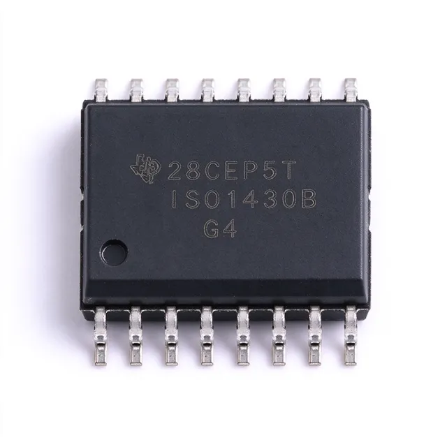
ISO1430BDW - 12Mbps Isolated RS-485/RS-422 | Texas Instruments
The Texas Instruments ISO1430BDW is an EMC-protected, galvanically isolated half-duplex RS-485 and RS-422 transceiver designed for industrial communication links. It supports signaling rates up to 12 Mbps and provides 5-kVrms reinforced isolation according to the manufacturer product-page description. The device is packaged in a 16-pin wide-body SOIC, making it suitable for high-speed half-duplex bus systems that require electrical separation between the host interface and the external communications bus. Its integrated isolation and EMC protection are intended to simplify industrial interface design, particularly when connected to remote sensors, controllers, test equipment, or process-monitoring systems. The ISO1430 family also supports RS-485 and RS-422 applications in harsh industrial environments, where bus pins may be exposed to electrostatic-discharge and electrical-fast-transient disturbances. The ISO1430BDW is a single-transceiver device, meaning one package provides one isolated half-duplex RS-485/RS-422 channel. Its 12-Mbps capability is substantially faster than the 500-kbps ISO141x family, while remaining below the 50-Mbps ISO145x family. This makes the ISO1430 a useful middle-speed choice when data throughput and EMI immunity matter more than maximum-rate signaling. Designers should confirm the exact electrical limits, isolation ratings, supply requirements, temperature range, and pin-level connection details in the Texas Instruments ISO1430 datasheet before layout. The SOIC package requires careful creepage and clearance planning around the isolation barrier, while the bus interface requires termination, protection, and grounding practices appropriate to the installed cable and system topology.
ISO1432BDW - 12Mbps Isolated RS-485/RS-422 Transceiver | TI
The Texas Instruments ISO1432BDW is an EMC-protected, galvanically isolated RS-485 and RS-422 transceiver designed for reliable full-duplex data communication. It supports data rates up to 12 Mbps and provides 5 kVrms isolation, making it suitable for industrial, communications, and equipment interfaces that require robust protection against electromagnetic interference and high-voltage ground potential differences. The device is supplied in a 16-pin SOIC package and is specified for operation from -40 °C to +125 °C. An isolated transceiver is a type of interface IC that combines a differential line driver and receiver with an internal isolation barrier. The isolation barrier separates the logic-side supply and signals from the bus-side interface, helping prevent ground loops and allowing communication between equipment located at different ground potentials. The ISO1432 belongs to the broader interface-IC and communication-transceiver hierarchy, with RS-485 and RS-422 differential signaling designed for noise-resistant data transfer over cables. The ISO1432BDW is identified as a one-channel full-duplex transceiver with EMC protection. Full-duplex operation provides separate transmit and receive paths, allowing simultaneous bidirectional communication when the system requires it. The 12 Mbps maximum signaling rate supports high-speed industrial links, while the 5 kVrms isolation rating provides a substantial barrier between the two sides of the interface. The manufacturer product information identifies the family as an RS-485 and RS-422 transceiver and describes it as EMC protected. The DW package designation identifies the 16-pin SOIC outline used by this orderable variant. The part is suitable for industrial equipment, factory automation, data acquisition, building controls, and other installations where the interface must withstand electrically noisy environments. The isolation barrier and EMC-focused design are particularly useful when long cables, switching converters, motors, relays, or grounded subsystems can introduce transients and potential differences into a communication link. Designers should verify the complete pinout, isolation requirements, bus termination, common-mode range, supply sequencing, and maximum exposed-pad or package thermal constraints against the manufacturer datasheet before production release. The 16-pin SOIC footprint should be matched exactly to the DW package drawing, and the logic-side and bus-side isolation domains must be treated as separate electrical domains. Cable shielding, chassis grounding, surge protection, and appropriate common-mode protection should be evaluated for the intended installation. This product data combines Texas Instruments family information, distributor availability references, package details, and verified comparison data for engineering selection. It is intended to help engineers identify whether the ISO1432BDW meets the required communication rate, isolation level, package, temperature range, and EMC-protection needs before comparing it with alternative isolated transceiver implementations.
ISO1432DW - 12Mbps Isolated Full-Duplex RS-485/RS-422 Transceiver | TI
The Texas Instruments ISO1432DW is an EMC-protected, 12-Mbps, full-duplex, 5-kVrms isolated RS-485 and RS-422 transceiver housed in a 16-pin SOIC (DW) package. The device integrates a galvanic isolation barrier with reinforced insulation rated at 5 kVrms, a 1/1 (one driver, one receiver) full-duplex channel, and TI's proprietary EMC hardening for industrial bus robustness. Operating from a 3 V to 5.5 V supply, it supports data rates up to 12 Mbps and replaces discrete opto-isolator plus transceiver solutions with a single IC. An isolated RS-485 transceiver is a galvanically-isolated differential line driver/receiver designed for TIA/EIA-485-A and TIA/EIA-422-A applications. Within a system hierarchy, it sits at the interface between a low-voltage controller (MCU, FPGA, DSP) and a long-distance, noise-prone industrial bus. The isolation barrier blocks high-voltage transients, ground-potential differences, and common-mode noise that would otherwise couple into sensitive digital or analog circuitry upstream. By eliminating external optocouplers and isolated DC/DC converters (when paired with an integrated power isolator companion), the ISO1432 simplifies BOM, reduces board area, and improves reliability versus discrete implementations. Key features include 5-kVrms reinforced isolation per UL 1577, 12 Mbps maximum signaling rate, 1/1 full-duplex topology with separate driver output (Y/Z) and receiver input (A/B) pins, integrated bus protection including IEC 61000-4-2 ESD (typically 8 kV contact / 15 kV air) and IEC 61000-4-4 electrical fast transient immunity, and a wide 3 V to 5.5 V supply range. The device operates across -40 °C to +125 °C, suiting outdoor, cabinet-mounted, and motor-drive environments. The 16-pin DW SOIC footprint provides a creepage/clearance distance consistent with reinforced insulation requirements, simplifying PCB layout for high-voltage spacing. Internally, the ISO1432 uses TI's silicon-oxide (SiO2) capacitive isolation barrier combined with an RS-485 transceiver die on each side. The high-speed differential driver delivers 1.5 V minimum output swing into a 54 Ω load per TIA/EIA-485, while the receiver offers 50 mV typical hysteresis and a 1/8-unit-load input impedance (allowing up to 256 nodes on the bus when used with other 1/8-load parts). The EMC hardening includes spread-spectrum OOK signaling across the barrier and integrated surge protection on the bus pins, eliminating the need for external TVS diodes in many applications. Typical applications include industrial programmable logic controllers (PLCs), factory automation and field-bus networks, motor-control inverter gate-driver communication, solar inverter H-bridge control interfaces, building-automation RS-485 trunks, and any microcontroller-to-bus interface requiring reinforced isolation. The wide temperature range also suits outdoor instrumentation and renewable-energy installations. When designing with the ISO1432, allocate at least 8 mm of creepage on the PCB beneath and between the SOIC package sides to preserve the 5 kVrms rating, and pair the part with a wide-Vin isolated DC/DC (such as the ISOW1044 or ISOW1412 companion families) when the bus side must remain powered during MCU brownouts. Decouple both VCC1 and VCC2 with 1 µF X7R ceramic capacitors placed within 2 mm of the supply pins to keep digital switching currents off the isolation barrier. This page synthesizes distributor pricing, drop-in alternatives, and practical design notes not found in the standalone manufacturer datasheet.
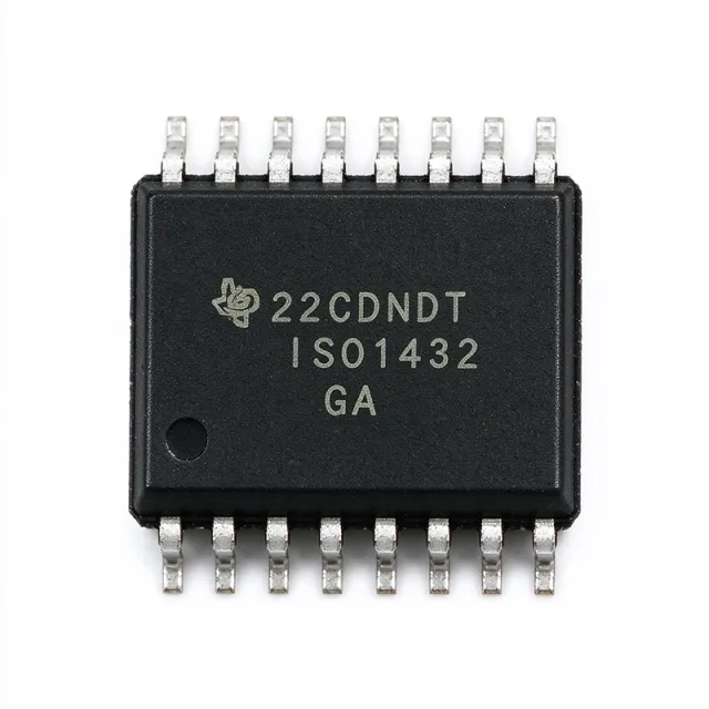
ISO1432DWR - 12Mbps Isolated Full-Duplex RS-485/RS-422 Transceiver | TI (Tape & Reel)
The Texas Instruments ISO1432DWR is an EMC-protected, 12-Mbps, full-duplex, 5-kVrms isolated RS-485 and RS-422 transceiver housed in a 16-pin SOIC (DW) package. The device integrates a galvanic isolation barrier with reinforced insulation rated at 5 kVrms, a 1/1 (one driver, one receiver) full-duplex channel, and TI's proprietary EMC hardening for industrial bus robustness. Operating from a 3 V to 5.5 V supply, it supports data rates up to 12 Mbps and replaces discrete opto-isolator plus transceiver solutions with a single IC. An isolated RS-485 transceiver is a galvanically-isolated differential line driver/receiver designed for TIA/EIA-485-A and TIA/EIA-422-A applications. Within a system hierarchy, it sits at the interface between a low-voltage controller (MCU, FPGA, DSP) and a long-distance, noise-prone industrial bus. The isolation barrier blocks high-voltage transients, ground-potential differences, and common-mode noise that would otherwise couple into sensitive digital or analog circuitry upstream. By eliminating external optocouplers and isolated DC/DC converters (when paired with an integrated power isolator companion), the ISO1432 simplifies BOM, reduces board area, and improves reliability versus discrete implementations. Key features include 5-kVrms reinforced isolation per UL 1577, 12 Mbps maximum signaling rate, 1/1 full-duplex topology with separate driver output (Y/Z) and receiver input (A/B) pins, integrated bus protection including IEC 61000-4-2 ESD (typically 8 kV contact / 15 kV air) and IEC 61000-4-4 electrical fast transient immunity, and a wide 3 V to 5.5 V supply range. The device operates across -40 °C to +125 °C, suiting outdoor, cabinet-mounted, and motor-drive environments. The 16-pin DW SOIC footprint provides a creepage/clearance distance consistent with reinforced insulation requirements, simplifying PCB layout for high-voltage spacing. Internally, the ISO1432 uses TI's silicon-oxide (SiO2) capacitive isolation barrier combined with an RS-485 transceiver die on each side. The high-speed differential driver delivers 1.5 V minimum output swing into a 54 Ω load per TIA/EIA-485, while the receiver offers 50 mV typical hysteresis and a 1/8-unit-load input impedance (allowing up to 256 nodes on the bus when used with other 1/8-load parts). The EMC hardening includes spread-spectrum OOK signaling across the barrier and integrated surge protection on the bus pins, eliminating the need for external TVS diodes in many applications. Typical applications include industrial programmable logic controllers (PLCs), factory automation and field-bus networks, motor-control inverter gate-driver communication, solar inverter H-bridge control interfaces, building-automation RS-485 trunks, and any microcontroller-to-bus interface requiring reinforced isolation. The wide temperature range also suits outdoor instrumentation and renewable-energy installations. When designing with the ISO1432, allocate at least 8 mm of creepage on the PCB beneath and between the SOIC package sides to preserve the 5 kVrms rating, and pair the part with a wide-Vin isolated DC/DC (such as the ISOW1044 or ISOW1412 companion families) when the bus side must remain powered during MCU brownouts. Decouple both VCC1 and VCC2 with 1 µF X7R ceramic capacitors placed within 2 mm of the supply pins to keep digital switching currents off the isolation barrier. This page synthesizes distributor pricing, drop-in alternatives, and practical design notes not found in the standalone manufacturer datasheet.

ISO1540D - 2.5kVrms I2C Digital Isolator | Texas Instruments
The Texas Instruments ISO1540D is a low-power, bidirectional I2C-compatible digital isolator providing galvanic isolation up to 2500Vrms. It supports data rates up to 1 Mbps from a 3V to 5.5V supply, housed in an 8-pin SOIC package (0.154in / 3.90mm width) with open-drain outputs rated 3.5mA sink current on Side 1 and 35mA on Side 2, operating from -40C to +125C. A digital isolator transfers digital signals across an isolation barrier, preventing DC and ground-loop current flow while allowing data to pass. Digital isolators are core building blocks in power management hierarchies, replacing optocouplers with higher speed, better reliability, longer life, and smaller footprint. The ISO1540D specifically addresses I2C buses, whose open-drain, bidirectional clock and data lines require specialized direction-handling logic that general-purpose digital isolators cannot provide. Key features include bidirectional SCL and SDA channels that isolate the I2C bus without external direction control, 1-MHz (fast-mode) operation, and 25kV/us common-mode transient immunity (CMTI) for robust operation in noisy power environments. The open-drain outputs integrate directly into standard I2C topologies with external pull-up resistors on both sides of the barrier. Technically, the ISO1540D uses TI capacitive isolation technology with a silicon dioxide (SiO2) barrier, delivering high isolation robustness and long-term reliability with a typical propagation delay of 67ns, preserving I2C timing margins. The wide 3V to 5.5V supply range allows 3.3V-to-5V logic domain crossing across the barrier. Typical applications include isolated I2C sensor interfaces in industrial automation, battery management systems (BMS), power supplies, motor drives, and medical monitoring equipment, where the ISO1540D separates control electronics from high-voltage or noisy power stages. Design tip: size pull-up resistors on both sides according to bus capacitance and the 1-Mbps data rate, and place 0.1uF decoupling capacitors close to both supply pins, as current pricing of roughly $2 to $4 per unit (as of 2026-08-29) makes it cost-effective to use one isolator per isolated bus segment.