انٹرفیس ICs
ذیلی زمرے
مصنوعات (2,300+)

SN65HVD10D - 3.3V RS-485 Transceiver 32Mbps | Texas Instruments
The Texas Instruments SN65HVD10D is a 3.3 V half-duplex RS-485 differential transceiver capable of 32 Mbps data rates, packaged in an 8-pin SOIC (D) package. The device combines a 3-state differential line driver with a differential input line receiver in a single monolithic IC, so a single pair of bus wires can carry data in both directions with one package footprint. An RS-485 transceiver is the physical-layer building block of balanced industrial communication. A differential bus rejects common-mode noise, supports long cable runs, and allows multiple nodes to share the same pair of wires in a multi-drop arrangement. The SN65HVD10 family operates from a single 3.3 V supply, which makes it a natural fit for 3.3 V microcontrollers, FPGAs, and industrial controllers that no longer include 5 V rails on the board. Key features include bus-pin ESD protection exceeding 16 kV HBM, compliance with the ANSI TIA/EIA-485-A and ISO 8482:1993 standards for balanced digital multipoint systems, and a 3-state driver output for bus segmentation. The half-duplex architecture uses separate driver-enable and receiver-enable inputs so transmit and receive direction can be controlled by a single GPIO direction pin. Device variants in the same family cover 1/2 and 1/8 unit-load options for denser multi-drop networks. Internally, the driver is a differential output stage with complementary A and B outputs, while the receiver is a differential comparator that produces a single-ended logic output. Because both halves share one 3.3 V rail and one ground, the ground reference between the transceiver and the cable shield must be handled carefully; a bus reference design typically adds fail-safe biasing resistors and a 120 ohm termination resistor at each physical end of the bus. Typical applications include industrial sensor and transducer buses, HVAC and building automation controllers, industrial gateways, remote I/O modules, and data-acquisition instrumentation running on 3.3 V logic. The 32 Mbps rating supports both legacy 115.2 kbps RS-485 networks and faster proprietary or Modbus RTU-over-TCP gateway links. When laying out the board, place the 0.1 uF and 1 uF decoupling capacitors directly across VCC and GND pins, keep the bus traces short and matched, and provide a chassis or surge reference path for the ESD structures on the bus pins. Avoid placing the transceiver in series with the signal path, and do not forget termination and fail-safe biasing on long or noisy segments. This page combines verified distributor pricing, package-accurate pinout data, drop-in alternatives drawn from the same TI bus-transceiver family, and practical layout notes that go beyond the manufacturer datasheet.
SN65HVD1176 - 40Mbps PROFIBUS RS-485 Transceiver | Texas Instruments
The Texas Instruments SN65HVD1176 is a half-duplex PROFIBUS RS-485 transceiver supporting signaling rates up to 40 Mbps in an 8-pin SOIC (D) package. The device meets or exceeds the requirements of ANSI TIA/EIA-485-A and is engineered for high-speed differential data transmission across twisted-pair networks. A PROFIBUS-compliant RS-485 transceiver is an interface IC that converts a single-ended TTL/CMOS logic signal from a UART, MCU, or ASIC into a balanced differential signal on a bus, and vice versa. RS-485 transceivers sit in the OSI physical layer between a microcontroller and the physical twisted-pair medium; PROFIBUS DP is a higher-level fieldbus protocol that uses the RS-485 physical layer at 12 Mbps. The SN65HVD1176 belongs to the hierarchy: RS-485 transceiver -> interface IC -> signal conditioning -> semiconductor. Compliance with EN 50170 (PROFIBUS) is a key differentiator from generic RS-485 parts. Key features include signaling rates up to 40 Mbps (well above the 12 Mbps PROFIBUS DP requirement), 1/5 unit load allowing up to 160 nodes on a single bus, low bus capacitance of 10 pF maximum for clean edges at high data rates, and a differential output voltage that exceeds 2.1 V across a 54 ohm load for robust noise margin. Driver and receiver enable pins support half-duplex operation and configurable bus states (active, driver-disabled, receiver-disabled, shutdown). The SN65HVD1176 uses a differential line driver with slew-rate-limited outputs to reduce EMI and reflections on improperly terminated buses. Internal fail-safe biasing on the receiver ensures a defined logic-high output when the bus is idle, open, or shorted - eliminating the need for external bias resistors. Wide operating supply range of 3.0V to 3.6V is compatible with 3.3V logic commonly used in industrial PLCs. Typical applications include PROFIBUS DP nodes, factory automation PLC backplanes, industrial sensor networks, motor drive communication links, and building automation gateways. The wide common-mode range (-7V to +12V) tolerates ground potential differences between nodes in large installations. A key design consideration is bus termination: PROFIBUS segments must be terminated with 220 ohm resistors at both ends (plus fail-safe bias) to suppress reflections at 12 Mbps. The device's low bus capacitance makes it well-suited to long stubs when used with proper termination. This page synthesizes drop-in alternatives, design considerations, and selection guidance not found in the manufacturer datasheet - enabling faster part selection and PCB layout reuse.
SN65HVD20D - 25 Mbps Extended Common-Mode RS-485 | TI
Texas Instruments SN65HVD20D is an extended common-mode RS-485 transceiver with a 4.5 V to 5.5 V supply, one transmitter, one receiver, and a maximum signaling rate of 25 Mbps in an 8-pin SOIC package. It combines half-duplex operation with a specified fault-protection range of -27 V to +27 V. According to the Texas Instruments SN65HVD2x family datasheet, the device exceeds typical RS-485 performance while meeting the requirements of the TIA/EIA-485-A standard. An RS-485 transceiver is a physical-layer interface IC that converts logic-level signals into a differential bus and receives differential bus signals back into CMOS-compatible data. Its hierarchy is transceiver → serial interface IC → differential line driver/receiver → communications interface. The SN65HVD20D is designed for industrial data links where long cables, grounded or unearthed systems, and differing ground potentials can place unusually large common-mode voltages on the bus. Three headline capabilities distinguish this device: its extended common-mode range, 25 Mbit/s maximum data rate, and -27 V to +27 V fault-protection window. The SN65HVD2x family also provides high ESD protection, wide receiver hysteresis, and failsafe operation. These features support reliable detection of small differential signals and recovery from excessive bus voltage, although the exact ESD rating, hysteresis voltage, and operating-temperature limits require confirmation in the manufacturer datasheet. The SN65HVD20D uses one differential driver and one differential receiver for half-duplex RS-485 communication. In a half-duplex network, transmit and receive functions share the same bus conductors, so system logic must control bus direction and avoid receiver contention. The supplied verification identifies a 5 V nominal operating range, 8-SOIC construction, one transmitter, one receiver, and a 25 Mbit/s maximum signaling rate; additional timing, supply-current, and propagation-delay values were not included in the source extract. Typical uses include factory automation, industrial instrumentation, building controls, process monitoring, and embedded serial networks. It is particularly relevant where a bus may be exposed to large common-mode offsets, electrostatic discharge events, or accidental fault voltage. The extended fault-protection feature helps the interface survive such transients, but external protection, termination, isolation, and grounding remain system-level design decisions. For a new PCB, place the transceiver near the bus connector, provide a continuous ground reference, route the differential pair as a tightly coupled pair, and use the bus protection specified by the application. Do not assume the -27 V to +27 V fault range eliminates the need for surge protection in an industrial installation, and verify decoupling requirements directly against the manufacturer datasheet. This page consolidates verified manufacturer and distributor information, a package-level replacement assessment, an eight-parameter comparison, and practical design notes. It distinguishes documented capabilities from missing electrical details so engineers can make a defensible RS-485 design decision without relying on unverified substitution assumptions.
SN65HVD21D - Extended Common-Mode RS-485 | Texas Instruments
Texas Instruments SN65HVD21D is a single-channel RS-422/RS-485 transceiver in an 8-pin SOIC package. The device combines one transmitter and one receiver in a half-duplex bus-line interface and provides extended common-mode operation for industrial, automation, instrumentation, and communications equipment. The SN65HVD21 family is designed to meet TIA/EIA-485-A requirements while adding high ESD protection, wide receiver hysteresis, and failsafe operation. Exact voltage, current, data-rate, temperature, and protection ratings are not included in the supplied verification data and therefore must be confirmed in the manufacturer datasheet before design release. An RS-485 transceiver is an interface IC that converts logic-level signals into a balanced differential bus and receives differential bus signals back into logic-level outputs. This class of device belongs to the interface IC hierarchy and ultimately supports the broader semiconductor and industrial communication ecosystem. Balanced signaling improves noise immunity by referencing the signal to differential line pairs rather than a single conductor, while extended common-mode capability helps a node remain functional when bus voltages exceed the common-mode range of a conventional transceiver. The SN65HVD21 family's verified features include high ESD protection, wide receiver hysteresis, and failsafe operation. High ESD protection is valuable in industrial environments where cables may be connected or disconnected during installation. Wide receiver hysteresis improves decision margin between logic states when a valid differential signal is present. Failsafe operation provides a defined receiver behavior for an inactive or undriven bus, helping system designers avoid ambiguous states in multi-node networks. The D-package suffix identifies an 8-pin SOIC implementation, while the P option is offered as a plastic through-hole package in the same family. This distinction matters to PCB designers: the SN65HVD21D uses a surface-mount footprint and cannot replace a through-hole SN65HVD21P without board changes. Although the SN65HVD21D and SN65HVD21DR may share the same electrical device and SOIC footprint, the latter is a packaging or orderable variant rather than a distinct engineering alternative. Typical uses include industrial RS-485 control links, factory automation equipment, remote sensor interfaces, building controls, and instrumentation networks. In a half-duplex arrangement, the transceiver's driver and receiver share the same differential pair, so system firmware and bus hardware must manage transmit and receive intervals without allowing multiple drivers to contend. Termination, biasing, grounding, and common-mode limits remain system-level constraints that cannot be selected from the limited values published in the supplied search results. Design with the manufacturer datasheet as the controlling authority for supply voltage, driver output current, receiver thresholds, propagation delay, maximum data rate, operating temperature, ESD ratings, and recommended external components. Keep bus-side traces away from sensitive signals, provide a solid ground reference, and verify that every attached node supports the same logic and baud rate. Confirm the exact pinout and exposed-pad requirements for the selected package rather than relying on generic SOIC drawings. This page consolidates the verified distributor and manufacturer information, distinguishes a true bus-interface alternative from packaging variants, and identifies missing electrical data explicitly. It provides selection and design guidance beyond a distributor listing while preserving the distinction between verified facts and parameters that require datasheet confirmation.

SN65HVD230DR - 3.3V CAN Transceiver 1Mbps 8-SOIC | Texas Instruments
The Texas Instruments SN65HVD230DR is a 3.3-V Controller Area Network (CAN) bus transceiver that supports data rates up to 1 Mbps and is compliant with the ISO 11898-2 High Speed CAN Physical Layer standard, housed in an 8-pin SOIC package with industrial -40C to +85C temperature rating. The device operates from a single 3.3-V supply (3.0 V to 3.6 V recommended) and integrates a differential driver and receiver pair with an RS pin for slew-rate control, enabling designers to balance bit rate against electromagnetic emissions. Bus pin ESD protection exceeds 16 kV HBM, and high input impedance supports up to 120 nodes on a single bus segment. A CAN transceiver is the physical-layer interface between a CAN protocol controller and the differential twisted-pair bus; it converts single-ended logic signals into the differential voltages defined by ISO 11898-2 and recovers received bits for the controller. Within the broader transceiver taxonomy (CAN transceiver -> serial interface IC -> interface IC -> signal path IC -> semiconductor), the SN65HVD230 sits alongside related interface standards like RS-485 and LIN, and is a low-power functional replacement for the legacy 5-V PCA82C250. Key features include a low-current standby mode that draws only 370 uA typical, an unpowered node that does not disturb the bus, and adjustable driver edge times via an external resistor on the RS pin. The wide common-mode receiver range of -2 V to 7 V improves immunity to ground shifts in long or noisy networks, and thermal shutdown protects the device from bus faults. Architecturally, the SN65HVD230 uses a bipolar CMOS-DMOS process that combines low quiescent current with the bus-driving strength required for 1 Mbps signaling. The RS-controlled slew rate reduces high-frequency harmonics that would otherwise couple into adjacent cables in dense industrial enclosures, which is why the part is favored in EMI-sensitive backplanes and in distributed sensor networks with cable harnesses of several meters. Typical applications include automotive body and chassis control modules, industrial automation and motor control, building automation (HVAC), telecom base-station housekeeping, and any 3.3-V microcontroller-based system that requires robust differential bus communication. The part is especially well suited to migrating legacy 5-V CAN designs down to 3.3-V rails without re-spinning the protocol layer. When designing with this device, terminate the CAN bus with a 120-ohm resistor at each end of the segment to suppress reflections and select the RS resistor appropriately: a low value (around 10 k-ohm) favors maximum bit rate, while a higher value (around 100 k-ohm) reduces slew rate and emissions. Always provide a solid ground return near the bus cable to keep common-mode noise within the receiver's -2 V to 7 V window. This page synthesizes distributor pricing, drop-in alternatives, and design guidance that complement, and in several areas go beyond, the manufacturer datasheet by capturing application experience from industrial and automotive CAN deployments.
SN65HVD231DR - 3.3V 1Mbps CAN Transceiver | Texas Instruments
Texas Instruments SN65HVD231DR is a 3.3 V controller area network transceiver with a maximum signaling rate of 1 Mbps, ISO 11898-2 compatibility, and an 8-pin SOIC package. It supports up to 120 nodes on a bus, provides bus-pin ESD protection exceeding 16 kV HBM, and includes adjustable driver transition times for improved signal quality. The SN65HVD231 variant is designed around an ultra-low-power sleep mode, making it useful in power-conscious CAN nodes. Its single-supply operation integrates a CAN controller-side interface with a physical bus-side driver and receiver. The device is intended for industrial, automotive-aftermarket, embedded control, and communications systems using CAN. Its high-input-impedance receiver helps support large networks, while controlled transition times can reduce radiated emissions and improve signal integrity. The transceiver is not a general-purpose logic device; CANH and CANL must be connected according to the bus topology and termination requirements. Design attention is required for supply decoupling, grounding, common-mode voltage, bus termination, and protection. This page combines verified manufacturer and distributor information with practical application guidance and clearly marks specifications that were not supplied.
SN65HVD232DR - 3.3V 1Mbps CAN Transceiver | Texas Instruments
The Texas Instruments SN65HVD232DR is a 3.3V single-channel CAN transceiver in an 8-pin SOIC package, supporting data rates up to 1Mbps and ISO 11898-2 high-speed CAN physical-layer compatibility. It combines a CAN transmitter, differential receiver, and 3.3V-compatible interface in a compact surface-mount package. A CAN transceiver is the physical-layer interface between a CAN controller and the differential CANH and CANL bus wires. It converts controller logic into dominant and recessive bus states, while converting differential bus voltage into a receive signal. The SN65HVD232 family is designed for systems using 3.3V DSPs or equivalent CAN controllers, with protection features intended to improve robustness in industrial and automotive-style networks. The SN65HVD232DR operates from a single 3.3V supply and supports CAN data rates up to 1Mbps. Its high receiver input impedance allows up to 120 nodes on a bus, according to the verified product and datasheet search results. The device also provides bus-pin ESD protection exceeding 16kV HBM, controlled driver output transition times for improved signal quality, and behavior suitable for unpowered nodes that do not disturb the bus. Compared with a 5V CAN transceiver, the SN65HVD232 family is intended for lower-voltage logic systems. The manufacturer search data identifies the principal 3.3V distinction as a lower dominant common-mode output voltage, by a few hundred millivolts, while the differential output voltage and recessive common-mode bias remain comparable. This makes the part suitable when the host controller, digital I/O, and system supply are designed around 3.3V. Typical applications include industrial automation equipment, motor-control systems, building automation, robotics, embedded control, vehicle electronics modules, and CAN-connected sensor or actuator networks. The transceiver is placed between a CAN controller and the CAN bus, with CANH and CANL routed as a differential pair and the logic-side interface connected to the controller. A key design consideration is confirming the complete transceiver pinout and logic levels in the manufacturer datasheet before layout release. Keep the CAN bus traces short, controlled-impedance where practical, and separated from noisy switching paths. Decoupling should follow the datasheet recommendations, and unused or unused-mode pins should be configured exactly as specified rather than inferred from generic CAN devices.
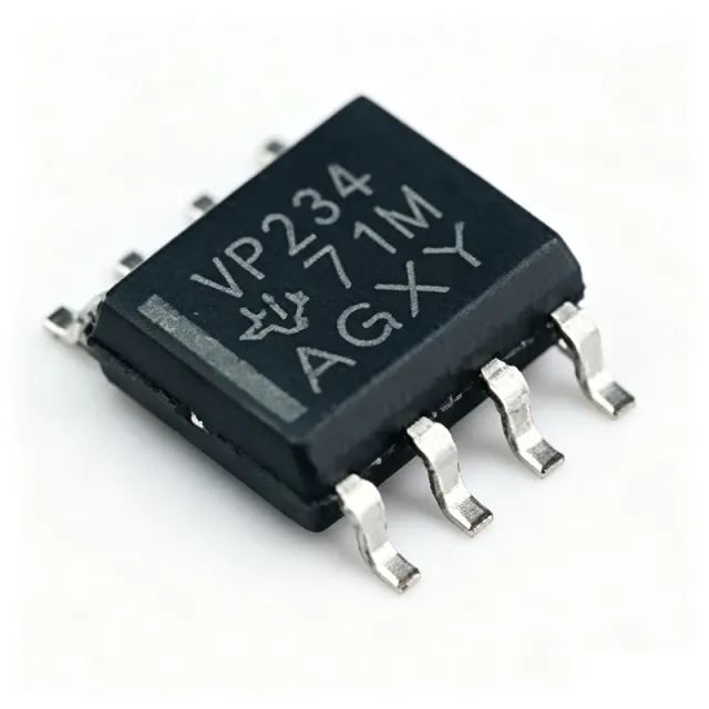
SN65HVD234DR - 3.3V CAN Transceiver 1Mbps w/ Sleep | Texas Instruments
The Texas Instruments SN65HVD234DR is a 3.3-V CAN (Controller Area Network) transceiver with sleep mode, offering data rates up to 1 Mbps compliant with ISO 11898 and packaged in an 8-pin SOIC (D) footprint rated from -40C to +125C. It supplies 3.3V logic with 5V-tolerant LVTTL I/Os, provides bus fault protection exceeding +/-36V, and withstands HBM ESD beyond 16 kV on bus pins. The device is the physical-layer interface between a CAN protocol controller and the differential CANH/CANL bus lines. A CAN transceiver is a physical-layer interface IC that bridges a digital protocol controller and a differential two-wire bus. In the broader interface IC taxonomy, it sits between logic-level MCUs/ASICs and the bus cable, implementing the differential driver, differential receiver, and bus fault protections required by the ISO 11898 standard. Within power-management and interface hierarchies it is part of the CAN/automotive-bus family of interface ICs, complementing isolated and high-speed variants. Key features include a wide common-mode input range extended to +/-12V, high input impedance supporting up to 120 nodes on the bus, and a multi-function RS pin that selects high-speed, slope-control, or low-power standby mode. Sleep-mode current is typically 0.05 uA and standby current is approximately 370 uA, allowing battery-powered nodes to remain always-on without draining the supply. Technically, the SN65HVD234DR uses a differential output stage with slew-rate control, thermal shutdown, and short-circuit protection on the bus pins. A dominant time-out function prevents a stuck controller from locking the bus. These protections allow reliable operation in electrically noisy automotive and industrial environments with ground-shift transients. Typical applications include automotive body control modules, industrial automation networks, building automation systems, and any 3.3V microcontroller-based CAN node where low quiescent current is required. Common companions are CAN-MC controllers such as the TMS320F28379D, ISO1050 isolated transceivers, and TCAN family devices. Design tip: terminate the bus with 120 ohm at both ends to suppress reflections, and use the RS pin to trade slew rate against EMI and loop latency. For multi-node networks, verify total node count and stub length per ISO 11898 guidelines. This page synthesizes distributor pricing, drop-in alternatives, and practical design notes not found in the manufacturer datasheet alone, organized to support both human engineers and AI search assistants.
SN65HVD23D - 25Mbps Extended CM RS-485 | Texas Instruments
The Texas Instruments SN65HVD23D is an extended-common-mode RS-485 transceiver rated for data rates up to 25 Mbps and supplied in an 8-pin SOIC package. It operates from a 5 V supply and supports an ambient operating-temperature range of -55°C to 125°C. The device combines one driver and one receiver, providing half-duplex communication over balanced cabling while addressing ground-potential differences commonly encountered in industrial systems. An RS-485 transceiver is an interface IC that translates between a single-ended logic signal and a differential differential-mode bus. The SN65HVD23 belongs to the broader RS-485 transceiver hierarchy, which also includes RS-422-compatible devices and provides noise immunity suitable for industrial communication, data acquisition, inverter control, and other long-cable applications. Its differential signaling, extended common-mode tolerance, and failsafe behavior help the system distinguish the intended signal despite bus noise and ground offsets. Key device characteristics include support for the TIA/EIA-485-A requirements identified in the manufacturer documentation, operation to 25 Mbps, a 5 V supply, and an extended operating-temperature range reaching 125°C. The HVD2x family also includes high ESD protection, wide receiver hysteresis, and failsafe operation. Wide receiver hysteresis reduces susceptibility to noise-induced state changes, while failsafe operation helps define the receiver output when the bus is idle or a driver is disconnected. The SN65HVD23D is a half-duplex transceiver, so the driver and receiver share the bus connection and an external mechanism is generally required to control which device transmits. Its extended common-mode range is especially useful where the transmitter and receiver grounds may be separated by ground-loop voltage or where the transceiver is used with electrical power inverters. Designers must nevertheless maintain a common reference within the limits of the device and preserve the specified termination and biasing arrangements. Typical uses include industrial inverter interfaces, factory automation equipment, building controls, data acquisition systems, and other multidrop RS-485 networks. At 25 Mbps, cable length, rise time, topology, and termination become increasingly important. Short, controlled-impedance connections are generally more suitable for maximum data rate than long unshielded cables, so the datasheet application information should guide network design. A key design consideration is the bidirectional half-duplex implementation. Because the driver is not automatically disabled when the receiver is active, incorrect control can cause bus contention and elevated power dissipation. An external transceiver-enable circuit, GPIO, or suitable bus controller should provide deterministic direction control. Decoupling should be placed close to the supply pins, while the differential pair should be routed with consistent geometry and controlled return paths. This page combines the verified manufacturer and distributor information, a conservative drop-in assessment, application guidance, and engineering-focused selection considerations. It also clearly identifies missing electrical details rather than estimating values that should be confirmed against the manufacturer datasheet before design release.

SN65HVD23P - 25 Mbps Extended CM RS-485 Transceiver | TI
The Texas Instruments SN65HVD23P is a half-duplex RS-422/RS-485 interface transceiver rated for data rates up to 25 Mbps and packaged in an 8-pin PDIP. Its extended common-mode voltage range spans -20 V to 25 V, exceeding the range required by the TIA/EIA-485-A standard, while reduced unit loading supports networks containing up to 256 nodes. An RS-485 transceiver is the physical-layer interface between a digital controller or microcontroller and a balanced, multipoint communication bus. It combines a differential line driver, a differential receiver, and driver-enable control in one package. In the hierarchy of electronic components, the SN65HVD23P is a bus transceiver within the interface IC category, bridging a logic-level UART or controller connection to a noise-resistant differential bus. Key features include a 25 Mbps maximum signaling rate, extended common-mode operation from -20 V to 25 V, receiver equalization for improved cable-length capability, and bus I/O protection exceeding 16 kV HBM. The reduced unit-load architecture allows up to 256 nodes on a bus, an important distinction from transceivers designed around one-half or one-eighth unit loads. The 8-pin PDIP package also provides through-hole mechanical compatibility for industrial and legacy control equipment. The transceiver combines a push-pull differential driver with a high-impedance differential receiver. Because it is a half-duplex device, the driver and receiver share the same bus pair, making the driver-enable function essential for preventing multiple transmitters from driving the bus simultaneously. The extended common-mode capability helps the receiver interpret differential signals correctly when bus nodes are separated by significant ground potential, although cable routing and grounding still determine practical noise immunity. Typical applications include industrial factory automation, motor controllers, building-automation equipment, remote sensor nodes, and industrial data acquisition. The part is particularly useful when a bus must tolerate ground offsets, longer cable runs, or more nodes than a standard RS-485 transceiver supports. Its 25 Mbps capability also suits high-rate point-to-point RS-422 links and short high-speed industrial bus segments. For PCB implementation, treat the differential bus as a controlled-impedance routed pair and keep the transceiver close to the connector or cable termination. Place termination resistors only at the physical ends of the bus. Verify the logic polarity of the driver-enable input in the host firmware because incorrect enable sequencing can cause contention or bus termination faults. This page combines the verified manufacturer and distributor information with engineering guidance covering common-mode range, bus loading, protection, package reuse, replacement constraints, and design trade-offs that are not presented as one consolidated decision source in the manufacturer product listing.
SN65HVD3082EDR - 200kbps Low-Power RS-485 | Texas Instruments
The Texas Instruments SN65HVD3082EDR is a half-duplex RS-485 transceiver designed for 5 V data-bus systems, supporting signaling rates up to 200 kbps in an 8-pin SOIC package. It combines one driver and one receiver with low active quiescent current of 0.3 mA and shutdown current of 1 nA, helping reduce power in distributed industrial, building-automation, and instrumentation networks. The transceiver is designed for balanced twisted-pair buses and supports up to 256 nodes at a 1/8 unit-load configuration. An RS-485 transceiver is an interface IC that combines differential line driver and receiver functions into a two-wire, half-duplex communication link. RS-485 belongs to the broader interface-IC hierarchy and is widely used where multiple distributed devices must communicate over a relatively long cable. Differential signaling improves common-mode noise rejection, while controlled transition times reduce unwanted emissions and help maintain reliable operation across industrial environments. The SN65HVD3082EDR provides one driver and one receiver, a 4.5 V to 5.5 V supply range, and TIA/EIA-485A compliance according to the retrieved manufacturer information. Its low-power architecture is especially useful when the transceiver must remain connected to a bus while minimizing standby consumption. The device also includes bus-pin ESD protection up to 15 kV, a feature important for physically exposed communication ports. Typical applications include industrial RS-485 networks, building-control equipment, factory automation, remote sensor nodes, and low-speed serial data acquisition. The half-duplex arrangement requires the design to manage transmit-enable direction control so that the driver does not contend with the receiver during reception. Bus termination, biasing, grounding, and cable routing remain essential parts of a reliable implementation. The key design consideration is ensuring that the external bus network and transceiver control logic match the application’s transmission direction. A 120-ohm termination resistor is commonly placed at each end of a properly terminated RS-485 cable, while fail-safe biasing should be designed for the system’s idle state. The SOIC-8 package simplifies assembly, but exposed bus pins require careful layout and protection planning. This product page combines verified manufacturer and distributor information, structured application guidance, and explicit data-availability markers for parameters not present in the retrieved source set. It is intended to support engineering comparison and sourcing without inferring unverified electrical values.

SN65HVD37D - 3.3V Full-Duplex RS-485 Transceiver | TI (Tape & Reel)
The Texas Instruments SN65HVD37D is a low-power, 3.3V full-duplex RS-485/RS-422 transceiver housed in a 14-pin SOIC package. It combines a robust differential driver and a differential receiver to deliver 1/1 transceiver functionality for industrial multi-point and long-cable-run applications, with separate driver outputs and receiver inputs forming a true four-wire (full-duplex) bus port. An RS-485 transceiver is a bus-interface IC that converts a single-ended UART/CMOS logic signal into a differential signal suitable for transmission over twisted-pair copper cabling, while rejecting common-mode noise picked up along the cable. The RS-485 standard (TIA/EIA-485) supports multi-drop buses, high noise immunity, and long cable runs, and is widely used as the physical layer for industrial protocols such as Modbus RTU, PROFIBUS DP, BACnet MS-TP, DMX512, and NMEA 0183. The HVD37 family belongs to the 3.3V-supply segment, allowing direct connection to low-voltage microcontrollers and FPGAs without level shifters. Key specifications include a 3.3V nominal supply (3V to 3.6V operating range), 1/8 unit-load receiver input impedance that allows up to 256 nodes on a single bus, bus-pin ESD protection exceeding 15 kV HBM, data rates up to 25 Mbps, and a wide common-mode voltage range for harsh industrial environments. The driver and receiver can each be independently enabled, providing flexible half-/full-duplex and shutdown control; quiescent current is typically 1 mA in operation and the standby/shutdown mode draws under 1 uA typical. High receiver hysteresis (typ. 60 mV) delivers robust noise immunity on long cables. Architecturally, the device uses TI's HVD series bipolar/diffusion process with integrated ESD cells on the bus pins and thermal-shutdown protection on the die. Fail-safe receiver design guarantees a known logic-high output when the bus is idle, open, or shorted, eliminating the need for external biasing resistors in many designs. The combination of 3.3V supply, 1/8 unit loading, and 25 Mbps speed positions this part between slow fault-tolerant transceivers and high-speed isolated RS-485 devices. Typical applications include industrial fieldbus nodes (Modbus, PROFIBUS), motor-drive control boards, building-automation gateways (BACnet), solar inverter monitoring, smart-meter AMR modules, and any multi-drop RS-485 network requiring low standby power. Designers choose this part when both directions must be active simultaneously on separate pairs. Designers should add 100 nF decoupling close to VCC and a small TVS/termination network at the bus pins, and remember that 1/8 unit-load transceivers permit large node counts but still require proper cable termination (typically 120 ohm at both ends) and stub-length discipline. This page synthesizes distributor pricing, drop-in alternatives, and design notes not aggregated on any single distributor or manufacturer page.
SN65HVD37DR - 3.3V Full-Duplex RS-485 Transceiver | TI
The Texas Instruments SN65HVD37DR is a low-power, 3.3V full-duplex RS-485/RS-422 transceiver housed in a 14-pin SOIC package. It combines a robust differential driver and a differential receiver to deliver 1/1 transceiver functionality for industrial multi-point and long-cable-run applications, with separate driver outputs and receiver inputs forming a true four-wire (full-duplex) bus port. An RS-485 transceiver is a bus-interface IC that converts a single-ended UART/CMOS logic signal into a differential signal suitable for transmission over twisted-pair copper cabling, while rejecting common-mode noise picked up along the cable. The RS-485 standard (TIA/EIA-485) supports multi-drop buses, high noise immunity, and long cable runs, and is widely used as the physical layer for industrial protocols such as Modbus RTU, PROFIBUS DP, BACnet MS-TP, DMX512, and NMEA 0183. The HVD37 family belongs to the 3.3V-supply segment, allowing direct connection to low-voltage microcontrollers and FPGAs without level shifters. Key specifications include a 3.3V nominal supply (3V to 3.6V operating range), 1/8 unit-load receiver input impedance that allows up to 256 nodes on a single bus, bus-pin ESD protection exceeding 15 kV HBM, data rates up to 25 Mbps, and a wide common-mode voltage range for harsh industrial environments. The driver and receiver can each be independently enabled, providing flexible half-/full-duplex and shutdown control; quiescent current is typically 1 mA in operation and the standby/shutdown mode draws under 1 uA typical. High receiver hysteresis (typ. 60 mV) delivers robust noise immunity on long cables. Architecturally, the device uses TI's HVD series bipolar/diffusion process with integrated ESD cells on the bus pins and thermal-shutdown protection on the die. Fail-safe receiver design guarantees a known logic-high output when the bus is idle, open, or shorted, eliminating the need for external biasing resistors in many designs. The combination of 3.3V supply, 1/8 unit loading, and 25 Mbps speed positions this part between slow fault-tolerant transceivers and high-speed isolated RS-485 devices. Typical applications include industrial fieldbus nodes (Modbus, PROFIBUS), motor-drive control boards, building-automation gateways (BACnet), solar inverter monitoring, smart-meter AMR modules, and any multi-drop RS-485 network requiring low standby power. Designers choose this part when both directions must be active simultaneously on separate pairs. Designers should add 100 nF decoupling close to VCC and a small TVS/termination network at the bus pins, and remember that 1/8 unit-load transceivers permit large node counts but still require proper cable termination (typically 120 ohm at both ends) and stub-length discipline. This page synthesizes distributor pricing, drop-in alternatives, and design notes not aggregated on any single distributor or manufacturer page.
SN65HVD50D - 25Mbps RS-485/RS-422 Transceiver | Texas Instruments
The Texas Instruments SN65HVD50D is a high-output, full-duplex RS-485 and RS-422 interface transceiver designed for reliable point-to-point and multipoint communications. It operates from a 4.5 V to 5.5 V supply, supports signaling rates up to 25 Mbps, and combines one driver with one receiver in an 8-pin SOIC package. The device includes selectable driver transition-time options for 1 Mbps, 5 Mbps, and 25 Mbps signaling, allowing designers to balance transmission distance, signal integrity, and electromagnetic compatibility requirements. An RS-485 transceiver is an interface IC that converts logic-level signals into differential bus voltages and receives differential bus signals back into logic-level outputs. This product belongs to the broader RS-485 transceiver family, which is part of the interface IC category and supports industrial, telecommunications, building automation, instrumentation, and data-communication equipment. The SN65HVD50D is appropriate where a system requires a dedicated full-duplex RS-485 or RS-422 interface rather than a half-duplex transceiver. Key features include 1/8 unit-load operation for networks containing as many as 256 nodes, bus-pin ESD protection exceeding 15 kV HBM, and a low-current standby mode with 1 µA typical standby current. The receiver provides 50 mV hysteresis, which helps improve noise immunity during differential signaling. The 25 Mbps maximum data rate makes the device suitable for high-speed data links where cable length and topology must be considered carefully. The SN65HVD50D is a single-channel transceiver with separate transmit and receive paths, allowing full-duplex communication. Its high-output driver is intended for driving differential cables and interconnects while maintaining robust signal margins. The manufacturer product page identifies the device as a High Output Full-Duplex RS 485 Driver and Receiver, while distributor listings identify the package as 8-SOIC and describe it as an RS-422/RS-485 interface IC. Typical applications include industrial control networks, factory automation equipment, instrumentation systems, building-control networks, and high-speed industrial data links. When selecting it, engineers should verify cable length, node count, termination, common-mode range, grounding, and connector requirements against the complete manufacturer datasheet before layout release. A practical design consideration is that the driver transition-time setting affects edge rate and therefore can influence EMI behavior. Keep the differential pair routed with controlled geometry, provide the required bus protection and termination, and validate the complete board-level signal integrity at the selected data rate. This page combines manufacturer and distributor information with application guidance, comparison criteria, and drop-in replacement findings to support faster engineering evaluation.
SN65HVD51D - 5Mbps Full-Duplex RS-485 Transceiver | Texas Instruments
Texas Instruments SN65HVD51D is a high-output, full-duplex RS-422/RS-485 interface transceiver with one driver and one receiver, a maximum signaling rate of 5 Mbps, a 4.5 V to 5.5 V supply range, and an 8-pin SOIC package. The device provides separate driver and receiver paths for balanced industrial communications. An RS-485 transceiver is an interface IC that converts logic-level signals into differential bus signals and converts received differential signals back into logic levels. It belongs to the communication-interface hierarchy: RS-422/RS-485 transceiver, differential line driver and receiver, interface IC, and semiconductor. This signal conversion allows equipment to communicate reliably over longer cable runs, especially in industrial environments where common-mode noise and ground-potential differences can disrupt single-ended signaling. Key features include a one-eighth unit-load option supporting as many as 256 nodes on a bus, bus-pin electrostatic-discharge protection exceeding 15 kV HBM, and optional driver output transition times for 1 Mbps, 5 Mbps, and 25 Mbps signaling. The SN65HVD51D also supports a low-current standby mode below 1 µA and provides glitch-free operation. Its high-output design is intended for industrial communication and data-transmission systems using balanced transmission lines. The SN65HVD51 family operates from a 5 V supply and is offered in an 8-pin SOIC package. The D ordering option is specified for operation from -40 °C to 85 °C. According to the Texas Instruments product information, the SN65HVD51, SN65HVD50, and SN65HVD52 are fully enabled and have no external enable pins, allowing continuous operation without external driver or receiver control. The D suffix identifies the 8-pin SOIC package rather than a different transceiver function. Typical applications include industrial automation controllers, factory data-acquisition equipment, remote sensor interfaces, building-control systems, and communications equipment operating in electrically noisy environments. Full-duplex operation permits simultaneous transmission and reception on separate differential pairs, while the one-eighth unit-load capability helps designers connect more nodes than a conventional one-unit-load receiver would support. When laying out a board, use a controlled-impedance differential pair for each bus direction, provide a continuous ground reference, and place termination, protection, and common-mode components at the physical bus interface. Supply decoupling should be placed close to the device. Because RS-485 communication quality also depends on cable characteristics, grounding, topology, and termination—not only the transceiver—validate the complete channel in the target environment. This page combines verified Texas Instruments product information, distributor availability references, cross-reference results, and practical engineering guidance. It also distinguishes the confirmed pin-compatible THVD1451 replacement from same-family Texas Instruments alternatives whose enable and electrical characteristics require board-level verification before substitution.
SN65HVD54D - 5 Mbps Full-Duplex RS-485 | Texas Instruments
The Texas Instruments SN65HVD54D is a high-output, full-duplex RS-485 driver and receiver with separate driver and receiver enables, operating from a single 5 V supply in a 14-pin SOIC (D) package. It supports signaling rates up to 5 Mbps, provides a 1/8-unit-load option for as many as 256 nodes on a bus, and includes bus-pin ESD protection exceeding 15 kV HBM. The device also offers a low-current standby mode with 1 µA typical standby current and selectable driver transition times optimized for 1 Mbps, 5 Mbps, and 25 Mbps signaling environments. An RS-485 transceiver is an interface integrated circuit that combines a differential line driver and differential receiver for balanced digital communications. It belongs to the RS-422/RS-485 transceiver hierarchy within interface ICs, where the driver translates logic-level signals into differential bus voltage and the receiver converts differential bus voltage back into a logic-level signal. Full-duplex operation provides separate paths for transmission and reception, making the SN65HVD54D suitable for systems that cannot share the same bus conductors in both directions. The SN65HVD54D provides one driver and one receiver, with independent enables that allow the system to place either side into a low-power state. Its high-output architecture is intended for demanding balanced-line links, while the selectable driver edge rates let engineers optimize signaling behavior for 1 Mbps, 5 Mbps, or faster communication links. The 1/8-unit-load receiver option can support up to 256 nodes, reducing the loading burden in large multi-node industrial systems. Bus-pin ESD protection exceeding 15 kV HBM adds an important ruggedness margin where cables and external connectors are exposed to electrostatic discharge. The device operates across the -40 °C to +85 °C temperature range in the SN65HVD54D ordering option. Its separate full-duplex driver and receiver structure is particularly useful when the transmitting and receiving nodes must remain active simultaneously. Typical uses include industrial factory automation, building-control networks, industrial instrumentation, motor-control systems, process monitoring, and other full-duplex RS-485 links. The 5 Mbps capability supports factory-floor communication, while the standby function can reduce consumption when a node is not communicating. Component placement and termination remain important because the transceiver does not eliminate the need for a balanced cable, appropriate bus topology, and correctly engineered termination. Designers should verify enable polarity in the host logic, place the device close to the bus connector, and provide protection appropriate to the installation environment. The internal high-impedance state supports controlled bus participation, but software and fault-management circuitry must still prevent multiple transmitters from driving the same bus at the same time. This page consolidates verified manufacturer and distributor information, package details, lifecycle attributes, replacement guidance, and application-oriented engineering context. It also distinguishes documented drop-in family options from alternatives that may require different packages or interface behavior, helping engineers shorten component-selection and PCB-validation work.
SN65HVD55D - 1Mbps Full-Duplex RS-485 | Texas Instruments
The Texas Instruments SN65HVD55D is a high-output, full-duplex RS-485 driver and receiver with enables, supporting data rates up to 1 Mbps and operation from -40°C to +85°C in a 14-pin SOIC package. It provides a 1/8-unit-load option for networks containing as many as 256 nodes, 50 mV receiver hysteresis for improved noise immunity, and bus-pin ESD protection exceeding 15 kV HBM. An RS-485 transceiver is a bidirectional communications interface that combines a differential line driver, a differential receiver, and associated enable controls. It belongs to the interface-IC hierarchy and enables robust communication over long, noisy cables by representing digital data as a differential voltage across a balanced pair of conductors. The SN65HVD55D uses separate driver and receiver paths, allowing full-duplex operation on a four-wire bus. Key features include a maximum data rate of 1 Mbps, 1/8-unit-load operation, and optional driver transition times intended for signaling rates of 1 Mbps, 5 Mbps, and 25 Mbps. The low-current standby mode consumes 1 µA, making the enables useful for power-conscious systems. Bus-pin ESD protection exceeding 15 kV HBM helps improve robustness where cables connect the transceiver to external equipment. The high-output architecture increases the amount of signal energy available on the bus, while the receiver's 50 mV hysteresis rejects noise within the transition region between differential output states. The device is suitable for RS-422 and RS-485 equipment where point-to-point or multipoint differential signaling is required. Its independent enable controls permit the driver and receiver to be switched according to the operating state of the connected system. Typical applications include industrial automation equipment, factory-floor controllers, building-control systems, data-acquisition equipment, communications modules, and external bus interfaces. In a full-duplex installation, the driver connects to one differential pair and the receiver connects to another pair, allowing simultaneous transmission and reception without sharing the same bus conductors. Designers should account for cable length, topology, termination, grounding, and the slew-rate option when selecting the device. The bus must remain within the transceiver's specified electrical limits, and unused inputs should be handled according to the manufacturer guidance. Enable sequencing should also prevent simultaneous bus contention where multiple nodes share a conductor pair. This product page combines the verified manufacturer description, distributor availability, package information, RS-485 operating characteristics, and documented family differences. It also provides application guidance and a structured comparison for engineers evaluating drop-in interface choices without adding unverified electrical claims.
SN65HVD61D - Single-Channel ControlNet Transceiver | Texas Instruments
Texas Instruments SN65HVD61D is a single-channel ControlNet physical-layer transceiver with one driver and one receiver, supplied in a 14-pin SOIC package. Designed for single-node operation and distributed stand-alone applications, it provides the circuitry required by ControlNet coaxial-based physical layers. Its pull-or-pull transmitter sinks current from a center-tapped transformer, supporting galvanic isolation between the transceiver circuitry and the external network interface. The combination of one integrated transceiver channel, transformer-compatible drive topology, and a compact 14-SOIC package makes the device applicable to industrial automation, controller, sensor, and factory-control networks. A ControlNet transceiver is a specialized interface IC that converts digital logic signals into a balanced physical-layer network connection and converts received network signals back into logic-level data. Within the product hierarchy, it belongs to the interface transceiver class, with ControlNet operation representing its defining protocol and physical-layer function. Its isolation-oriented transmitter arrangement is particularly useful where system designers require a transformer-based link between the transceiver and a coaxial cable network. The SN65HVD61D integrates one driver and one receiver into a single channel. The manufacturer describes the transmitter as a pull-or-pull arrangement that sinks current from a center-tapped transformer rather than driving the cable directly. This architecture allows the external transformer to establish the physical signal coupling and galvanic isolation. The 14-SOIC package supports conventional surface-mount assembly while providing a practical pin count for a complete single-channel interface. The primary system benefit is functional consolidation: one device contains both sides of the ControlNet physical-layer connection. This can reduce the number of separate interface components required for a single-node or stand-alone node. The galvanic-isolation capability provided by the center-tapped transformer arrangement is also important in industrial environments where isolation between the electronic circuitry and external cabling is a system requirement. Actual isolation voltage, data rate, supply range, and timing limits must be confirmed in the manufacturer datasheet before final qualification. Typical use cases include ControlNet-compatible programmable logic controllers, industrial automation controllers, remote I/O nodes, factory sensor interfaces, motor-control supervisory nodes, and distributed process-monitoring equipment. In each case, the SN65HVD61D handles the local logical transceiver function while a suitable center-tapped transformer connects the device to the ControlNet physical layer. The primary design consideration is transformer and network compatibility. The external center-tapped transformer must match the device's electrical and timing requirements, and its wiring must preserve the intended isolation boundary. PCB signal integrity, return paths, bypass-capacitor placement, and connector or cable characteristics also require careful implementation because the transceiver communicates through a coupled physical layer rather than a direct point-to-point logic interface. This page consolidates the verified manufacturer description, distributor identification, package information, sourcing links, and practical engineering guidance. It also distinguishes the SN65HVD61D from family ordering variants and identifies where additional electrical, timing, compliance, or lifecycle data must be obtained from the authoritative manufacturer documentation.

SN65HVD70DGSR - 3.3V Full-Duplex RS-485 400kbps Transceiver, 10-VSSOP | Texas Instruments
The Texas Instruments SN65HVD70DGSR is a 3.3 V, full-duplex RS-485 transceiver rated for data rates up to 400 kbps, integrating ±12 kV IEC 61000-4-2 contact discharge ESD protection, in a 10-pin VSSOP (DGS) PowerPAD package. The device pairs one differential driver with one differential receiver, each with dedicated input/output pins, enabling simultaneous transmit and receive on a four-wire bus typical of RS-422 and full-duplex RS-485 networks. The driver includes active-high enable control and the receiver includes active-low enable control, allowing a sub-5 µA standby current when both functions are disabled. A transceiver of this class is the physical-layer interface between a UART/MCU and a differential twisted-pair cable in industrial multipoint networks. The SN65HVD70 extends TI's RS-485 portfolio as a low-power, robust 3.3 V member of the SN65HVD7x family, suitable for half- and full-duplex links across factory floors, building automation, and motor-drive backplanes. As a line transceiver it sits hierarchically below the protocol layer (Modbus, PROFIBUS, DMX512) and above the cable plant, converting CMOS/TTL logic levels into the differential A/B signaling defined by TIA/EIA-485-A and TIA/EIA-422-B. Key features include ±30 kV HBM ESD on the bus pins, a wide 3.0 V to 3.6 V supply range, a 1.8 V to 5 V logic interface (no level shifter needed in 1.8 V systems), open-circuit, short-circuit, and bus-idle fail-safe receiver inputs, and a thermal-shutdown protected driver. The 10-pin VSSOP package with thermal pad keeps the footprint compact while supporting industrial -40 °C to +125 °C operation. The device uses a precision differential architecture with large receiver hysteresis (typically 50 mV) to reject common-mode noise on long cable runs. The wide common-mode range of -7 V to +12 V tolerates ground potential differences between nodes, and the 1/8 unit-load option permits up to 256 nodes on a single bus. Slew-rate limiting reduces EMI reflections on unterminated stubs. Typical applications include industrial multi-drop RS-485 networks, building-automation backbones, motor-control command links, point-of-sale peripherals, and full-duplex RS-422 point-to-point data links. The device is well matched to long cable runs with proper 120 Ω termination at both ends. When designing with this part, place 100 nF decoupling capacitors within 2 mm of VCC and use a 120 Ω termination resistor at each end of the bus. Do not leave unused driver outputs floating - tie them to GND through a resistor. Maintain a 1/8 unit-load budget when scaling beyond 32 nodes. This page synthesizes distributor pricing, drop-in alternatives, and practical design notes not found in the manufacturer datasheet, including cross-vendor equivalents and full intent coverage in the FAQ for engineers planning second-source qualification.
SN65HVD72D - 3.3V 250kbps Half-Duplex RS-485 | Texas Instruments
The Texas Instruments SN65HVD72D is a 3.3 V half-duplex RS-485 transceiver with IEC ESD protection and a maximum signaling rate of 250 kbps, packaged in an 8-pin SOIC (D) package. It combines one RS-485 driver and one RS-485 receiver in a single integrated circuit, making it suitable for bidirectional industrial communication links using differential bus wiring. The part is identified by Texas Instruments as an active product with an operating temperature range of -40 °C to 125 °C and RoHS-compliant construction. An RS-485 transceiver is an interface IC that translates between a logic-level UART or digital signal and a differential RS-485 bus. The differential architecture supports noise-resistant communication over longer cable runs than single-ended signaling, while the half-duplex arrangement allows the same pair of bus conductors to support both transmission and reception. In this device, the 3.3 V supply and 250 kbps data rate suit embedded systems, industrial controllers, sensors, and equipment using low-speed field-bus links. Key verified characteristics include a 3.3 V supply, 250 kbps maximum signaling rate, half-duplex operation, RS-422/RS-485 transceiver functionality, and IEC ESD protection. The SOIC-8 package provides a compact surface-mount footprint for industrial control boards and communication modules. The device is marketed for demanding industrial applications where robust bus interfacing and protection are important. The SN65HVD72D integrates the physical-layer functions needed to connect a microcontroller or programmable logic controller to a differential RS-485 network. Designers should pay attention to bus biasing, termination, grounding, cable length, and the exact logic-control requirements of the selected family variant. The manufacturer product page and part-details page are the authoritative sources for ordering information, electrical characteristics, and package details. Typical uses include industrial automation equipment, remote sensor interfaces, building-control systems, instrumentation, and embedded serial networks. Compared with lower-speed or more highly integrated interface solutions, the SN65HVD72D provides a focused 250 kbps half-duplex RS-485 solution with ESD protection in a standard 8-pin SOIC package. This page combines verified manufacturer and distributor information with practical selection guidance, pricing context, and application notes for engineers evaluating the SN65HVD72D.
SN65HVD73D - 20Mbps Full-Duplex RS-485 | TI
The Texas Instruments SN65HVD73D is a 3.3 V full-duplex RS-485/RS-422 transceiver with a 20 Mbps maximum data rate, ±12 kV IEC ESD protection, and individual driver and receiver enables in a 14-pin SOIC (D) package. The device integrates one driver and one receiver, supports a 3 V to 3.6 V supply range, operates across -40°C to +125°C, and provides 70 mV receiver hysteresis. An RS-485 transceiver is a physical-layer interface IC that converts low-voltage digital logic signals into differential bus signals and reconstructs logic-level data from a differential bus. It belongs to the transceiver hierarchy within interface ICs and enables robust, point-to-point or multidrop communication over longer distances than single-ended logic interfaces. Full duplex means the driver and receiver can operate simultaneously on separate differential pairs. The SN65HVD73D's principal features include a 20 Mbps data rate, 70 mV receiver hysteresis, separate active-high driver enable and active-low receiver enable controls, and ±12 kV IEC-rated ESD protection. Its 3 V to 3.6 V operating range is appropriate for 3.3 V systems. The broad -40°C to +125°C temperature range supports industrial and extended-temperature equipment when the complete system qualification permits it. The integrated driver and receiver provide one RS-485/RS-422 communication channel in full-duplex configuration. Separate enables allow the transmitter and receiver to be disabled independently, and the manufacturer product page states that standby current can be reduced below 5 µA when both functions are disabled. A common ground reference and carefully terminated differential wiring remain necessary for reliable operation. Typical applications include industrial control networks, factory automation equipment, data acquisition systems, building-automation controllers, and communications between a host controller and a peripheral transceiver. The 20 Mbps capability supports high-speed point-to-point links, while the ±12 kV IEC ESD rating helps protect external bus connectors in electrically noisy environments. Designers should follow the manufacturer datasheet for transceiver pinout, termination, fail-safe biasing, and differential routing. Keep the RS-485 differential pair routed as a controlled-impedance pair, minimize stub lengths, place termination only where required by the bus topology, and verify grounding and surge-protection requirements for the installed environment. This product summary consolidates verified manufacturer and distributor information, supply parameters, design guidance, and replacement constraints into one engineering-focused reference. It also clearly distinguishes verified specifications from electrical values that require confirmation from the complete datasheet before schematic release.
SN65HVD73DGS - 3.3V Full-Duplex RS-485 20Mbps | Texas Instruments
The Texas Instruments SN65HVD73DGS is a 3.3 V full-duplex RS-485 transceiver with integrated active-high driver enable and active-low receiver enable pins, supporting data rates up to 20 Mbps in a 10-pin VSSOP (DGS) package. It integrates a differential driver, a differential receiver, and 12 kV IEC ESD protection on bus pins, operating from a single 3.3 V supply across the industrial -40°C to +125°C temperature range. The device is designed for high-speed, half-duplex-to-full-duplex RS-485 networks in industrial automation, motor control, and point-to-point data links. A RS-485 transceiver is a balanced differential line driver/receiver IC that converts a single-ended TTL/CMOS logic signal into a differential signal conforming to the TIA/EIA-485-A standard, enabling robust multi-drop communication over twisted-pair cable with common-mode voltage tolerance up to ±25 V and cable lengths up to 1200 m at reduced data rates. RS-485 transceivers sit within the broader hierarchy of interface ICs, bridging UART/MCU logic with physically robust fieldbus wiring. The SN65HVD73DGS belongs to the 3.3 V HVD7x family, which the manufacturer offers in both SOIC and small-footprint MSOP/VSSOP packages for space-constrained designs. Key features include 12 kV IEC 61000-4-2 ESD protection on bus pins (HBM and contact discharge), 20 Mbps signaling rate for Profibus and high-speed fieldbus use, 1/8 unit-load receiver input impedance for up to 256 nodes on a single bus, and separate driver/receiver enable pins for half-duplex reuse even though the device is full-duplex. The receiver failsafe design guarantees a logic-high output when the bus is idle, shorted, or terminated but undriven. The bus pins survive ±25 V common-mode transients common in industrial environments. Architecturally, the SN65HVD73DGS uses a 3.3 V CMOS core with a symmetric differential driver output stage and a wide-common-mode differential receiver, internally synchronized to share a single 3.3 V supply rail. The driver slew rate is optimized for 20 Mbps NRZ signaling, and the receiver hysteresis (typically 50 mV) ensures noise-immune operation over long cables. Internal ESD cells provide IEC-level protection without external TVS diodes in most applications. Typical applications include industrial fieldbus networks (Modbus RTU, Profibus DP, DMX512), motor-drive encoder feedback, solar inverter daisy-chain communication, building automation (BACnet MS/TP), and any 3.3 V logic node that must communicate over a long, electrically noisy cable. Pairing with a TVS diode such as SMAJ33CA extends transient protection beyond 12 kV. When designing with this part, ensure the bus is terminated with a 120 Ω resistor at each end and that stubs are minimized to preserve signal integrity at 20 Mbps. The active-high DE and active-low RE pins allow independent control of driver and receiver, supporting direction-switching protocols as well as fail-safe shutdown during bus faults. Decouple VCC with a 0.1 µF ceramic capacitor placed within 5 mm of the supply pin.
SN65HVD73DGSR - 3.3V Full-Duplex RS-485, 20Mbps, 12kV ESD | TI
The Texas Instruments SN65HVD73DGSR is a 3.3-V full-duplex RS-485 transceiver with separate driver and receiver pins, 20 Mbps signaling rate, and ±12-kV IEC 61000-4-2 contact ESD protection, housed in a 10-pin MSOP/VSSOP (DGS) package. The wide common-mode voltage range makes the device suitable for multi-point RS-485 / RS-422 bus applications over long cable runs in industrial, building automation, and motor-control networks. A RS-485 transceiver is a physical-layer interface IC that converts between a low-voltage UART/logic-level signal on the controller side and a balanced differential signal on the bus side. Full-duplex (a.k.a. 4-wire RS-485) uses separate differential pairs for transmit and receive, allowing simultaneous two-way communication. The SN65HVD73 belongs to the broader family of half- and full-duplex RS-485 transceivers -> differential line transceivers -> interface ICs -> integrated circuits in the data-communication hierarchy defined by TIA-485 / EIA-422 standards. Key features include 3.3-V single-supply operation (compatible with modern low-power MCUs and FPGAs), 20 Mbps maximum data rate, ±30-kV HBM and ±12-kV IEC 61000-4-2 contact-discharge ESD on bus pins, large receiver hysteresis for noise immunity in harsh industrial environments, 1/8 unit-load support that lets up to 256 nodes share one bus, and separate driver-enable (DE) and receiver-enable (RE) pins for direction control and half-duplex reuse. Operating temperature spans -40 °C to +125 °C. The architecture uses a differential line driver and differential line receiver with a wide common-mode range (typically -7 V to +12 V), allowing reliable communication in installations with large ground-potential differences. Internal slew-rate control and low bus-current loading support PROFIBUS, DMX512, and similar multi-drop protocols at 20 Mbps without external components. Typical applications include industrial field-bus nodes, motor encoder feedback links, building-automation gateways, solar inverter monitoring, and point-to-point backplane links between 3.3-V controllers. The wide common-mode range and IEC-grade ESD simplify compliance with industrial EMC requirements without external TVS arrays. When designing with this device, place the 100 nF VCC bypass capacitor as close to pin 10 as possible and use 120 Ω termination only at the two physical ends of the bus. Leave the middle of the bus unterminated to avoid loading reflections. The DE and RE pins let the host power-gate the part in sleep-mode designs by de-asserting both enables. This page synthesizes distributor pricing, drop-in alternatives from the TI SN65HVD7x family and cross-brand RS-485 ICs in the VSSOP-10 footprint, and practical design notes not found in the manufacturer datasheet alone.
SN65HVD75D - 3.3V 20Mbps RS-485 Transceiver | Texas Instruments
Texas Instruments SN65HVD75D is a 3.3 V half-duplex RS-485 transceiver with IEC ESD protection and a maximum signaling rate of 20 Mbps, housed in an 8-pin SOIC package. It supports operation from -40°C to 125°C and accepts 5 V-tolerant logic inputs compatible with 3.3 V or 5 V controllers. An RS-485 transceiver is an interface IC that combines a differential line driver and differential receiver, allowing digital data to be transmitted reliably over balanced, multipoint communication buses. The SN65HVD75 belongs to the transceiver hierarchy of interface ICs, differential line-driver and receiver circuits, and industrial communication semiconductors. Its half-duplex configuration permits a shared pair of conductors to carry data in either direction, but only one direction at a time. The SN65HVD75D operates from a 3.3 V supply, reaches 20 Mbps, and provides IEC ESD protection on the bus pins. Its logic interface supports 3.3 V and 5 V controllers, which simplifies connection to mixed-voltage digital systems. The wide -40°C to 125°C temperature range also makes the device suitable for industrial environments where commercial-temperature interface ICs may be inadequate. Exact ESD ratings, receiver thresholds, and electrical limits must be confirmed in the manufacturer datasheet. Each device combines a differential driver and differential receiver operating from one 3.3 V power supply. The bus pins are designed for robust ESD-event handling, including Human Body Model and IEC Contact Discharge protection. The manufacturer datasheet also identifies 250 kbps, 20 Mbps, and 50 Mbps signaling-rate options across the SN65HVD7x family, with 20 Mbps specifically associated with the SN65HVD75. Typical uses include industrial automation controllers, factory data buses, industrial instrumentation, building automation, and communications equipment operating on RS-485 networks. Its 20 Mbps capability supports high-speed half-duplex links, while 5 V-tolerant logic inputs ease interfacing with both 3.3 V and 5 V controllers. The half-duplex arrangement also requires careful direction-control design because the driver and receiver share the same bus pair. When designing the circuit, place a 100 nF ceramic bypass capacitor close to the supply pins and use a 3.3 V source capable of supporting the transceiver's operating current. The manufacturer recommends the TPS76333 for a suitable 3.3 V supply and the SN6501 for isolated power-supply designs. Bus routing should minimize stubs and maintain controlled differential impedance. This page combines verified manufacturer and distributor information, transparent pricing-status notes, same-family replacement analysis, and practical RS-485 design guidance. It also distinguishes verified electrical facts from parameters that still require confirmation against the complete SN65HVD7x manufacturer datasheet.