مصنوعات (19,000+)

AM6528BACDXEA - Dual Cortex-A53 1.1GHz Sitara MPU | TI
AM6528BACDXEA

AM6528BACDXEA - Dual Cortex-A53 1.1GHz Sitara MPU | TI

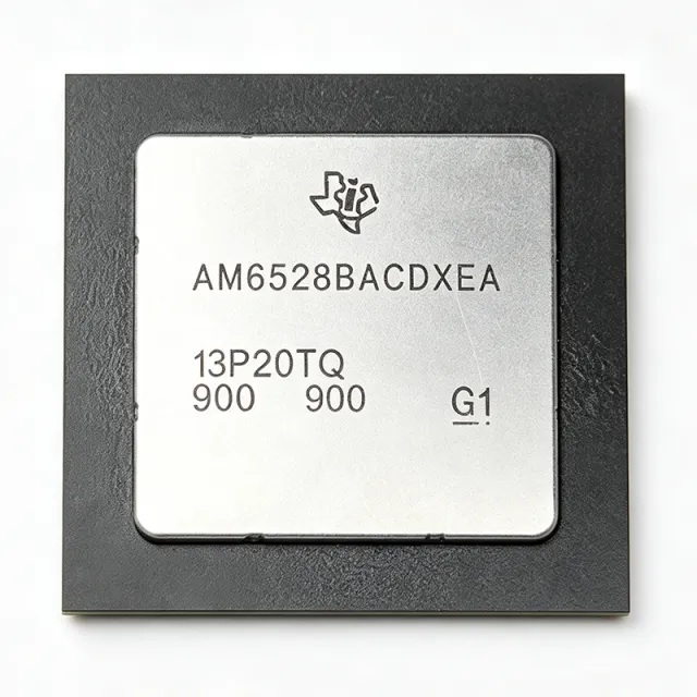
The Texas Instruments AM6528BACDXEA is a Sitara microprocessor (MPU) integrating dual Arm Cortex-A53 cores running at 1.1 GHz, a dual Arm Cortex-R5F MCU subsystem at 400 MHz, and Gigabit-class PRU-ICSS industrial communication subsystems, housed in a 784-pin FCCSP (ACD) package measuring 23x23 mm and rated for -40C to +105C operation. A microprocessor unit (MPU) is the central computation engine of an embedded system, sitting above microcontrollers (MCU) in the processing hierarchy but below application processors in complexity. Modern industrial MPUs like the AM6528 combine an applications-class Arm Cortex-A53 cluster for Linux-based software with a real-time Cortex-R5F lockstep-capable MCU subsystem, enabling a single chip to run both a high-level OS and deterministic real-time control tasks - a partitioning that previously required two separate devices. Key differentiating features include the PRU-ICSSG (Programmable Real-time Unit Industrial Communication Subsystem) with three Gigabit instances, supporting industrial Ethernet protocols such as EtherCAT, PROFINET, and EtherNet/IP in hardware with deterministic latency. A 3D graphics acceleration engine (SGX544 class) enables HMI and visualization workloads. The Cortex-R5F subsystem includes features intended to support functional-safety goals per the TI datasheet for the AM654x/AM652x family (Silicon Revision 2.1 documentation). Architecturally, the AM6528 belongs to the Sitara AM65x generation, built on TI's proven Cortex-A53/R5F heterogeneous multicore approach. The A53 cluster executes Linux or RTOS software, while the R5F cores handle time-critical control loops and safety monitoring, communicating through shared on-chip interconnect and memory subsystems. Typical applications include industrial PLCs and motor drive control heads, factory automation gateways with multi-protocol industrial Ethernet, HMI panels with 3D graphics, and building/energy automation controllers where -40C to +105C operation is required. When designing with this part, plan power sequencing for the multiple core rails and allocate DDR memory bandwidth carefully between the A53 and R5F subsystems; TI provides reference designs and power estimation tools in the AM65x documentation set. This page synthesizes distributor pricing, same-family drop-in alternatives, and practical design notes not found in the manufacturer datasheet.

RFQ رابطہ
AT32F403ARGT7 - 240MHz Cortex-M4F MCU 1MB Flash | Artery
AT32F403ARGT7

AT32F403ARGT7 - 240MHz Cortex-M4F MCU 1MB Flash | Artery

The Artery Technology AT32F403ARGT7 is a 32-bit ARM Cortex-M4F microcontroller with FPU running at up to 240 MHz, featuring 1 MB embedded Flash and 224 KB SRAM, housed in a 64-pin LQFP (10x10 mm) surface-mount package. A microcontroller unit (MCU) is a single-chip embedded processor that integrates a CPU core, memory, and peripherals such as timers, ADCs, and communication interfaces onto one die. Within the embedded systems hierarchy, the MCU sits below application processors (MPU/SoC) and above simple logic ICs, and this part belongs to the general-purpose high-performance MCU family built on the ARM Cortex-M architecture. Key differentiating specifications include the 240 MHz maximum core clock (well above the 72-168 MHz class of typical STM32F1/F4 counterparts), 1 MB of embedded Flash with sLib secure library protection, 17 timers, and 51 GPIO pins. Operating voltage spans 2.6 V to 3.6 V and the junction temperature range is -40C to +105C, covering industrial and automotive-adjacent environments. Technically, the AT32F403A series combines a single-precision floating-point unit (FPU) and DSP instructions with an advanced process node that Artery leverages to reach 200-240 MHz computing speeds. Peripherals include 3 x 12-bit ADCs, 20 communication interfaces including USBFS, multiple USART/SPI/I2C/CAN blocks, and a flexible clock control mechanism that supports both built-in and external Flash execution. Typical applications include FPV drone flight controllers, industrial motor control, communication modules and gateways, and consumer electronics where STM32F103-class pinouts are required at higher performance and lower cost. The AT32 family emerged as a proven STM32 alternative during the chip shortage and is widely used as a pin-to-pin upgrade path. Design consideration: because the 240 MHz core draws more dynamic current than 72 MHz Cortex-M3 parts, budget decoupling capacitance and PCB power-plane copper accordingly, and verify that your flash accelerator/wait-state settings match the higher clock in firmware. This page synthesizes distributor pricing, drop-in alternatives, pinout data, and practical design notes not found together in the manufacturer datasheet.

RFQ رابطہ
AT32F407VGT7 - 240MHz Cortex-M4 MCU 1MB Flash | Artery
AT32F407VGT7

AT32F407VGT7 - 240MHz Cortex-M4 MCU 1MB Flash | Artery

The Artery AT32F407VGT7 is an ARM 32-bit Cortex-M4 microcontroller with FPU and DSP instructions, operating up to 240 MHz, integrating up to 1 MB dual-bank Flash and 224 KB SRAM in a 100-pin LQFP package (14x14 mm, 0.5 mm pitch). A microcontroller (MCU) is a single-chip computer containing a processor core, program memory (Flash), data memory (SRAM), and a rich set of on-chip peripherals. The Cortex-M4 family targets high-performance embedded applications that require deterministic real-time control, DSP for audio/signal processing, and a single-precision Floating Point Unit (FPU) for efficient math. Within the power-management and embedded hierarchy, this part sits as: Cortex-M4 -> ARMv7-M architecture -> 32-bit MCU -> embedded processor -> semiconductor. The AT32F407 line is engineered by Artery as a cost-effective alternative to mainstream M4 families, with faster core clocks and dual-bank Flash for safer firmware updates. Key features include 240 MHz core speed, single-precision FPU, DSP extensions, 1 MB Flash (dual-bank option with sLib security library), 224 KB SRAM, three 12-bit ADCs (3 MSPS), two 12-bit DACs, USB 2.0 FS host/device/OTG, 10/100 Ethernet MAC, two CAN 2.0B interfaces, SDIO, FSMC, and up to 17 timers. Communication peripherals include I2C, SPI, I2S, USART and UART, totalling up to 21 communication interfaces. Operating voltage is 2.6 V to 3.6 V with an industrial -40C to +105C junction temperature range. The architecture combines an M4 core with tightly-coupled SRAM, multi-layer AHB/APB buses, and a DMA controller for low-CPU-overhead data movement. The dual-bank Flash supports in-application programming (IAP) without halting execution, and the sLib security region protects intellectual property. The 240 MHz clock enables deterministic control loops and DSP workloads that are typically out of reach for lower-end MCUs. Typical applications include industrial motor control (BLDC, FOC drives), USB/Ethernet connected gateways, USB Type-C power-delivery controllers, consumer audio with DSP effects, human-machine interface (HMI) panels with LCD via FSMC, drones/flight controllers, and IoT edge nodes. The combination of CAN, Ethernet and USB makes it well-suited to automotive aftermarket and industrial automation products. When designing with this MCU, ensure the external quartz or resonator load capacitors match the AT32 reference design (typically 8-20 pF), and place the on-board 1uF/100nF decoupling network within 3 mm of every VDD/VDDA pin. Always configure the option-byte write protection for production units to lock the bootloader region from accidental erase during field updates. This page synthesises distributor pricing, drop-in alternatives, and practical design notes that complement the manufacturer datasheet DS_AT32F407_V2.04_EN.pdf and the LCSC stock snapshot.

RFQ رابطہ
AT32UC3A0512-ALUT - 32-bit AVR32 MCU 66MHz 512KB Flash LQFP-144
AT32UC3A0512-ALUT

AT32UC3A0512-ALUT - 32-bit AVR32 MCU 66MHz 512KB Flash LQFP-144

The Microchip Technology AT32UC3A0512-ALUT is a high-performance, low-power 32-bit AVR32 RISC microcontroller based on the UC3 A0 system-on-chip architecture, operating at frequencies up to 66 MHz and packaged in a 144-pin LQFP (20x20 mm). The device integrates 512 KB of Flash and 64 KB of SRAM, combined with a rich set of peripherals including a 10/100 Ethernet MAC, full-speed USB 2.0 with embedded host capability, I2S audio interface, and a stereo audio D/A converter. An MCU (Microcontroller Unit) is a single-chip computer that combines a processor, memory, and programmable I/O. The 32-bit AVR32 UC3 family belongs to the broader category of embedded microcontrollers -> RISC processors -> semiconductors -> integrated circuits, designed for cost-sensitive embedded applications with particular emphasis on low power consumption, high code density, and high computational throughput. The AVR32 core implements a compact single-cycle RISC instruction set including DSP extensions, with the AT32UC3A0512 reaching approximately 1.38 DMIPS/MHz. Key specifications include 1.65 V to 3.6 V supply voltage operation, 66 MHz maximum CPU clock, 512 KB on-chip Flash program memory, 64 KB SRAM, integrated 10/100 Mbps Ethernet MAC, USB 2.0 full-speed On-The-Go controller, multi-layer AHB bus architecture, and a built-in audio DAC with I2S interface. The device supports external memory bus interfaces and provides extensive connectivity for embedded networking, audio, and human-machine-interface designs. The AVR32 UC3 core uses a Harvard-style architecture with separate instruction and data paths to the Flash and SRAM subsystems, enabling single-cycle instruction fetch and high deterministic interrupt latency. The integrated audio DAC and I2S make the part particularly well-suited for consumer audio applications, while the Ethernet MAC and USB OTG target industrial connectivity and embedded host stacks. The architecture includes read-modify-write atomic bit manipulation and DSP instruction extensions for signal-processing workloads. Typical applications include industrial Ethernet gateways, USB audio peripherals, point-of-sale terminals, smart energy metering, motor control front-ends, and embedded HMI panels. The combination of high-performance 32-bit compute with on-chip audio and networking peripherals enables the application to consolidate multiple discrete ICs into a single chip, reducing BOM cost and PCB footprint. Design considerations for this device include thermal management of the 20x20 mm LQFP-144 footprint, careful PCB layout for USB and Ethernet differential pairs, and adequate decoupling near the multiple VDD pins. Engineers should consult the AVR32 UC3 Technical Reference Manual for detailed peripheral programming guidance and the datasheet's electrical characteristics section before committing to a layout. This page synthesizes distributor pricing, an Octopart inventory view, Microchip cross-reference guidance, and practical design notes not found in the manufacturer datasheet, supporting both initial component evaluation and long-term re-purchase decisions.

RFQ رابطہ
AT32UC3C0512C - 32-bit AVR MCU 512KB Flash 66MHz | Microchip
AT32UC3C0512C

AT32UC3C0512C - 32-bit AVR MCU 512KB Flash 66MHz | Microchip

The Microchip (formerly Atmel) AT32UC3C0512C is a 32-bit AVR32 UC3 microcontroller delivering 66 MHz CPU performance with 512 KB Flash and 64-68 KB SRAM, housed in a 144-pin LQFP (20x20 mm) industrial-grade package. The device is engineered for industrial and automotive-grade control applications, with hardware dedicated to fast communication, motor control, and deterministic real-time response. A built-in single-precision floating-point unit (FPU) and DSP instruction extensions accelerate math-heavy control loops without burdening the core. An MCU (microcontroller unit) is a compact, self-contained computer on a single IC that integrates a CPU core, non-volatile program memory, working RAM, and a rich set of peripherals. The AT32UC3C0512C belongs to the 32-bit MCU category within the broader hierarchy of microcontrollers, embedded processors, and finally semiconductors. It targets motor-control and industrial-automation designs where deterministic latency and high analog integration matter more than raw clock speed. Key features include 512 KB Flash program storage, on-chip SRAM, full-speed USB 2.0 with OTG, 10/100 Ethernet MAC with MII/RMII, multiple USART (SPI/LIN mode capable), an Inter-IC Sound (I2S) controller, up to 16-bit ADC, and FlashVault code protection for IP security. A peripheral event system and 4-channel DMA offload the CPU, while an interrupt controller with autovector handling keeps latency predictable under heavy event load. The architecture pairs the AVR32 RISC core (including DSP and SIMD-friendly instructions) with hardware dedicated to power-conversion feedback loops: high-resolution PWM, motor-control timers, and synchronized analog comparators. This combination enables field-oriented control (FOC) algorithms and tight torque/velocity loops on a single chip, eliminating the need for external DSPs. Typical applications include industrial motor drives (BLDC, PMSM, stepper), automotive body and chassis ECUs, factory-automation PLCs, smart-grid metering, USB-to-Ethernet gateways, and embedded audio interfaces. The wide operating temperature range and FlashVault protection also make it suitable for secure connected nodes and industrial IoT edge controllers. Designers should size external decoupling carefully (1 µF + 100 nF near each supply pin), keep analog and digital ground returns separated, and use the on-chip DMA to keep ISR latency bounded. For motor-control firmware, the Atmel AVR32 framework and ASF provide production-ready FOC and PFC reference implementations. This page synthesizes Microchip product-page information, datasheet doc9166, distributor stock data, drop-in alternatives, and practical design notes not found in the manufacturer datasheet alone.

RFQ رابطہ
AT32UC3C0512C-ALUT - 32-bit AVR UC3 512KB Flash MCU | Microchip
AT32UC3C0512C-ALUT

AT32UC3C0512C-ALUT - 32-bit AVR UC3 512KB Flash MCU | Microchip

The Microchip Technology AT32UC3C0512C-ALUT is a 32-bit AVR UC3 C-series microcontroller featuring a 66 MHz AVR32 RISC core, 512 KB of in-system programmable Flash and 64 KB SRAM, housed in a 144-pin LQFP (20x20 mm, industrial -40C to +85C) package supplied in tray. The device targets industrial and automotive control applications with a focus on fast communication interfaces and motor control peripherals. An MCU (Microcontroller Unit) is a single-chip computer that integrates a CPU core, program and data memory, peripherals, and I/O. The AT32UC3 family belongs to the broader taxonomy of embedded microcontrollers within the semiconductor category, designed for deterministic, real-time control tasks. The 'AVR32 UC3 C' label specifies the 32-bit AVR32 RISC architecture (32-bit -> microcontroller -> embedded processor -> semiconductor), making it suitable for code-density-critical and signal-processing workloads. Key features include a 1.5 Msps 12-bit ADC (8 channels with dual sample-and-hold for simultaneous current/voltage sensing), single or dual CAN interfaces, Full-Speed USB 2.0 with On-The-Go host capability, NAND Flash and SDRAM external memory controllers, PWM channels with dead-time insertion for motor drive, and an MII/RMII 10/100 Ethernet MAC. The integrated media-independent interface (MII) and reduced MII (RMII) provide direct PHY connectivity without external glue logic. The architecture pairs a high-performance AVR32UC core with a Peripheral DMA Controller (PDCA) and a multi-layer High-Speed Bus Matrix, enabling parallel data movement between ADC, PWM, communication peripherals and memory without CPU intervention. This is essential for high-bandwidth motor control and audio streaming loops. The Nanotrace debug interface supports both JTAG and single-pin aWire debug through the RESET pin. Typical applications include industrial motor drives (BLDC/PMSM FOC), automotive body and chassis controllers, USB audio peripherals, CAN-connected sensor nodes, and Ethernet-enabled industrial gateways. The AT32UC3C0512CAU-ALUT variant is the Audio licensed-firmware IP version of the same silicon. When designing with this MCU, plan Pinout 144-LQFP PCB escape carefully because of the high pin count and 0.5 mm pitch; allocate at least four PCB layers with dedicated power and ground planes. Ensure the brown-out detector and watchdog timer are enabled for automotive-grade reliability. This page synthesizes Microchip datasheet extracts, same-package UC3C family variants, and design considerations not consolidated in the datasheet alone.

RFQ رابطہ
AT32UC3C0512C-ALZR - 32-bit AVR MCU 512KB Flash Automotive LQFP-144 | Microchip
AT32UC3C0512C-ALZR

AT32UC3C0512C-ALZR - 32-bit AVR MCU 512KB Flash Automotive LQFP-144 | Microchip

The Microchip Technology (formerly Atmel) AT32UC3C0512C-ALZR is an AVR32 UC3 C-series 32-bit RISC flash microcontroller integrating 512KB of Flash, 68KB of SRAM, and a hardware floating-point unit, housed in a 144-pin LQFP package (20x20 mm) and qualified to AEC-Q100 grade 1 for automotive control applications. It runs at 66 MHz core clock, supports 3.3V and 5V operating voltages, and is optimised for fast serial interfaces and field-oriented motor control. A microcontroller (MCU) is a single-chip computer that combines a CPU core, program memory (Flash), volatile memory (SRAM), and a rich set of on-chip peripherals (timers, communication, ADC, PWM, GPIOs). Within the broader system hierarchy, this part belongs to embedded microcontroller → 32-bit MCU → RISC MCU → automotive-grade MCU → semiconductor IC. The UC3 C-series specifically targets motor-control and industrial-control subsystems requiring deterministic PWM generation, fast ADC sampling, and CAN/LIN connectivity. Key features of the AT32UC3C0512C-ALZR include a 7-channel peripheral event controller, a 4-channel 12-bit ADC capable of simultaneous dual-sample conversion, programmable analog comparators with window detection, a Multi-purpose Timer Counter (TC) module with quadrature decoding, full-speed USB 2.0 device, two CAN controllers, four USARTs, and FlashVault code-protection for secure firmware IP. The hardware FPU accelerates single-precision math used in field-oriented control (FOC) algorithms. The device uses a Harvard-cache architecture with separate code and data memories to maximise throughput, and integrates dedicated motor-control peripherals such as the Pulse Width Modulation Controller (PWMC) and Quadrature Decoder (QDEC). AEC-Q100 grade 1 qualification ensures operation across -40C to +125C and resilience to automotive EMC profiles, making the part suitable for under-hood applications. Typical applications include industrial servo drives, automotive HVAC blower and pump controllers, BLDC and PMSM motor control, power-tool inverter control, field-oriented control of three-phase motors, and CAN/LIN node ECUs. The combination of FPU and motor-control peripherals removes the need for an external DSP in low-power-control designs. When designing with this MCU, budget Flash and SRAM carefully because the part does not include external memory bus, so all firmware must fit in the on-chip 512KB Flash and 68KB SRAM. Use the on-chip QTouch library for capacitive touch acquisition, and add CAN bus transceivers (e.g., MCP2551) and 12V-tolerant ESD diodes on automotive harnesses. This page synthesises distributor pricing from DigiKey, Mouser and Octopart, identifies same-brand and cross-brand drop-in alternatives, and adds practical design notes not found in the manufacturer datasheet, giving engineers a one-stop engineering summary.

RFQ رابطہ
AT80C32X2-RLTUM - 8-Bit 8051 ROMless MCU, 40/20MHz, 44-VQFP | Microchip
AT80C32X2-RLTUM

AT80C32X2-RLTUM - 8-Bit 8051 ROMless MCU, 40/20MHz, 44-VQFP | Microchip

The Microchip (formerly Atmel) AT80C32X2-RLTUM is an 8-bit ROMless 80C51/80C52-compatible microcontroller IC operating at 40 MHz (or 20 MHz in the lower-voltage range) in a 44-pin VQFP (10x10 mm) package. It features four 8-bit I/O ports (32 I/O lines), three 16-bit timer/counters, a full-duplex UART, and 256 bytes of on-chip scratchpad RAM. As a ROMless derivative of the AT89C family, external program memory is required, making this part ideal for memory-intensive or field-upgradeable firmware designs. A microcontroller (MCU) is a single-chip computer containing a CPU, memory, and peripherals. The 8051 architecture is a foundational 8-bit ISA widely used in industrial control, automotive body electronics, and consumer appliances. Within the taxonomy: 8051 -> 8-bit MCU -> microcontroller -> embedded IC -> semiconductor. The AT80C32X2 belongs to the ROMless segment of this family, where code is fetched from external EPROM/Flash rather than internal non-volatile memory, simplifying code development during prototyping. Key features include dual clock domain support (0 to 40 MHz at 5 V, 0 to 20 MHz at 3 V), six interrupt sources with two priority levels, on-chip analog watchdog, power-saving idle and power-down modes, and an extended 16-bit program counter supporting up to 64 KB of external code space. The -RLTUM suffix designates the 44-pin VQFP industrial-temperature (-40C to +85C) operating range, lead-free RoHS-compliant package. Architecturally, the AT80C32X2 uses CMOS technology with static design, allowing the clock to be stopped without losing internal state. The four-port parallel I/O structure provides 32 flexible bidirectional lines, and the on-chip oscillator supports external crystal, ceramic resonator, or external clock source. The non-volatile code execution model (external ROM) suits designs where code must be updated in the field without re-spinning silicon. Typical applications include industrial control systems, motor drive interfaces, sensor data acquisition nodes, building automation controllers, and legacy 8051 firmware migration designs where code density or revision history exceeds internal Flash capacity. It is also well-suited as a drop-in replacement for legacy Atmel 80C32 systems requiring an RoHS-compliant upgrade path. When designing with this device, ensure the EA pin is tied low to force external code fetch (ROMless), and provide proper bus-cycles timing accounting for any external memory wait states. The VQFP-44 footprint requires standard surface-mount assembly with the exposed-pad thermal pad soldered to a copper pour for thermal dissipation in enclosed industrial enclosures. This page synthesizes verified distributor stock data, same-brand drop-in VQFP-44 alternatives, and practical 8051 design notes not consolidated in any single source.

RFQ رابطہ
AT89C51AC3-S3SUM - 8-Bit 80C51 MCU, 64KB Flash, 60MHz | Microchip
AT89C51AC3-S3SUM

AT89C51AC3-S3SUM - 8-Bit 80C51 MCU, 64KB Flash, 60MHz | Microchip

The Microchip Technology (formerly Atmel) AT89C51AC3-S3SUM is a high-performance 8-bit 8051-family microcontroller with 64KB of in-system programmable flash, 2KB boot flash, 2KB EEPROM, and 2048 bytes of ERAM, offered in a 52-pin PLCC package rated for the industrial temperature range. A microcontroller (MCU) is a single-chip computer that integrates a CPU core, program memory, working RAM, and a rich set of programmable peripherals on one die. The 8051 architecture, originally introduced by Intel in 1980 and now widely licensed through Microchip/Atmel, sits in the broader product hierarchy: microcontroller -> embedded MCU -> 8-bit MCU -> CISC processor -> semiconductor. The AT89C51AC3 belongs to the 89C family (flash-based 8051), which is itself a derivative of the original 80C51, an industry standard for decades of legacy embedded designs. Key features include a 60 MHz maximum core clock (or 20 MHz in X2 mode), full MCS-51 instruction-set compatibility, three-level program memory lock, ISP/IAP (in-system and in-application programming), a 10-bit ADC, dual hardware PWM channels, a hardware watchdog, and a CAN 2.0B controller that distinguishes this part from the older AT89C51/C52. The 52-pin PLCC (plastic leaded chip carrier) gives designers 36 programmable I/O lines plus dedicated analog, PWM, and CAN pins, with a JEDEC-standard J-lead footprint that supports both socketed and surface-mount assembly. Typical applications include industrial automation controllers, motor drives (via the hardware PWM and 10-bit ADC), automotive body and chassis ECUs (CAN bus), smart metering, building automation, and any brownfield 8051 design that needs to retain legacy code while adding modern flash memory and on-chip peripherals. The 5V industrial-grade supply simplifies integration into legacy 5V rails, and the AEC-Q100-style temperature range suits outdoor and automotive environments. When designing with the AT89C51AC3, ensure that the SST89E516RD-style bootstrap loader pins are connected to a UART for ISP, and observe the 5V supply range. Because the part uses the 8051 CISC core, throughput-sensitive paths should leverage the X2 mode or migrate code to the faster SFR access patterns available in the AC3 silicon revision.

RFQ رابطہ
AT89C51CC01UA-SLSUM - 8-bit CAN MCU, 32KB Flash, 40MHz, PLCC-44 | Microchip
AT89C51CC01UA-SLSUM

AT89C51CC01UA-SLSUM - 8-bit CAN MCU, 32KB Flash, 40MHz, PLCC-44 | Microchip

The Microchip Technology AT89C51CC01UA-SLSUM is an enhanced 8-bit 80C51 AT89C CAN microcontroller with 32 KB of in-system programmable Flash, 2 KB of boot Flash, 2 KB of EEPROM, and 1.2 KB of internal RAM, operating up to 40 MHz (20 MHz) in X2 mode) and supplied in a 44-pin PLCC (16.6 x 16.6 mm) package. It is the first member of the Microchip/Atmel CAN family of 8-bit MCUs designed specifically for CAN network nodes. A CAN microcontroller is a microcontroller that integrates a hardware Controller Area Network (CAN) peripheral on-chip, allowing the device to communicate directly on CAN bus segments used in automotive, industrial, and building-automation networks. The AT89C51CC01UA belongs to the broader 8051 (MCS-51) family, which is one of the longest-lived 8-bit MCU architectures; devices in this hierarchy range from bare 8051 cores through 8051 derivatives, embedded microcontrollers, and on to system-on-chip devices that integrate peripherals such as CAN, ADC, and PWM. Key features include a fully static 8051 core, 32 programmable I/O lines, three-level program memory lock for code protection, an endurance rating of 1,000 write/erase cycles per Flash sector, hardware CAN 2.0B controller, ISP/IAP via bootloader, and an industrial operating temperature range of -40 C to +85 C. The PLCC-44 package provides a robust through-hole-style surface-mount footprint that is easy to prototype with standard PLCC sockets. Typical applications include automotive body and chassis ECUs, industrial CAN-based sensor/actuator nodes, HVAC control modules, building-automation gateways, and CAN-to-UART bridges. The integrated CAN peripheral is one of the three most differentiated capabilities of this device, making it attractive in designs that need a single-chip CAN node without an external CAN controller. When designing with the AT89C51CC01UA, ensure the oscillator circuit follows the manufacturer reference design and that adequate decoupling (typically 100 nF ceramic per VCC pair plus bulk 10 uF) is placed close to the supply pins. The PLCC-44 socket should be of the proper polarization type to avoid pin reversal damage during field service. This page synthesizes verified distributor data, drop-in compatible parametric and behavioral notes, and engineering design considerations not found in the manufacturer datasheet. Pricing is shown as of 2026-10-07 and reflects real-time inventory from authorized distributors.

RFQ رابطہ
AT89C51CC03CA-RDTUM - 8-bit CAN MCU, 64KB Flash, 40MHz | Microchip
AT89C51CC03CA-RDTUM

AT89C51CC03CA-RDTUM - 8-bit CAN MCU, 64KB Flash, 40MHz | Microchip

The Microchip Technology AT89C51CC03CA-RDTUM is an 8-bit 80C51-core microcontroller with an integrated full CAN (Controller Area Network) controller, 64KB of in-system programmable Flash, 2KB of boot Flash, 2KB of SRAM, and a 40MHz maximum CPU clock (6.66 MIPS), housed in a 64-pin VQFP (10x10) tray-packaged package. The integrated CAN 2.0A/B controller, large Flash complement, and automotive-friendly 3.0V to 5.5V supply range make it a drop-in workhorse for industrial CAN nodes, automotive body and chassis ECUs, and embedded networking appliances where MCS-51 firmware migration matters. An 8-bit CAN MCU is a microcontroller that combines the deterministic, low-overhead 8051 instruction set with an on-chip CAN protocol engine for in-vehicle and industrial networks. It sits in the embedded hierarchy between classic 8051 microcontrollers (no networking) and 32-bit CAN microcontrollers (more performance, more power, more code complexity). The AT89C51CC03CA belongs to Microchip's AT89C51CC03 family, which extends the legacy AT89C51 line by adding CAN, ISP/IAP, and a hardware bootloader for field-upgradeable nodes. Key features include 64KB of in-system programmable Flash with 1000 write/erase cycles, 2KB SRAM for stack and frame buffers, 2KB boot Flash with dedicated bootloader, 2048 bytes of EEPROM for non-volatile parameters (CAN node ID, calibration), 32 programmable I/O lines, three 16-bit timer/counters, a programmable hardware watchdog, full CAN 2.0A/B controller, hardware SPI, UART with enhanced framing, and X2 mode for up to 40MHz equivalent throughput from a 20MHz crystal. The wide 3.0V to 5.5V operating range supports both 3.3V and 5V CAN transceivers and bus rails. Architecturally the device uses the standard 12-clock-per-instruction MCS-51 core and adds dual Flash banks plus a true hardware CAN state-machine rather than a bit-banged software stack. In X2 mode, every peripheral cycle is divided by two, allowing the CPU to perform one instruction per external clock cycle and reach 300ns instruction timing at 20MHz external crystal, doubling effective throughput without redesigning firmware. Typical applications include CAN nodes in industrial fieldbus and DeviceNet systems, automotive body controllers, HVAC and instrument-cluster slaves, sensor and actuator modules with CAN connectivity, building-automation gateways, and any embedded 8051 firmware base that needs an in-place migration path to CAN. The 64-pin VQFP (10x10) footprint is the same land pattern as the rest of the AT89C51CC03 family, which simplifies PCB reuse. When designing with this device, ensure that the unused I/O pins are configured as outputs or pulled up to reduce supply current; ground the unused CAN RX input when CAN is not used. Verify that the CAN baud-rate prescaler, oscillator accuracy, and bit-timing configuration support the chosen bus length, because these directly affect sample point and EMC robustness. This page synthesizes distributor pricing, same-family drop-in alternatives, and practical design considerations for the AT89C51CC03CA-RDTUM not found in the manufacturer datasheet alone.

RFQ رابطہ
AT89C51CC03CA-RLTUM - 8-bit 8051 MCU 64KB Flash CAN VQFP-44 | Microchip
AT89C51CC03CA-RLTUM

AT89C51CC03CA-RLTUM - 8-bit 8051 MCU 64KB Flash CAN VQFP-44 | Microchip

The Microchip AT89C51CC03CA-RLTUM is an 8-bit 8051-family microcontroller with an integrated full CAN (Controller Area Network) controller, 64 KB of in-system programmable Flash, 2.25 KB of RAM, and 2 KB of EEPROM, housed in a 44-pin VQFP package. It executes the standard 80C51 instruction set at up to 40 MHz (X1 mode), and in X2 mode a 20 MHz external crystal reaches a 300 ns machine cycle, doubling effective throughput for compute-bound nodes. An 8051 microcontroller is a CISC 8-bit MCU architecture originally introduced by Intel in 1980 and now widely produced as a license-free core by several vendors. The 8051 sits within the broader hierarchy of microcontrollers -> embedded controllers -> semiconductor ICs and is widely deployed in industrial, automotive, and consumer nodes where deterministic behavior, low cost, and a mature toolchain outweigh the need for high-performance 32-bit cores. Devices with on-chip CAN are specifically positioned for automotive body and chassis networks, industrial fieldbus, and building-automation backbones where a CAN 2.0B controller simplifies bus arbitration. The AT89C51CC03CA integrates a full CAN 2.0B controller (15 message objects, programmable bit timing up to 1 Mbit/s), three 16-bit timer/counters, a hardware watchdog, dual UARTs, SPI, and a 10-bit ADC. With 1,000 write/erase cycle endurance on Flash, three-level program memory lock, and 4 KB of boot Flash for in-application re-programmability over UART or CAN, the device targets field-upgradable nodes and CAN bootloader implementations. The 32 programmable I/O lines on the 44-pin VQFP expose most of the 8051 peripheral set without external glue logic. Typical applications include CAN nodes in automotive body ECUs (door modules, seat controllers, lighting), industrial CANopen / DeviceNet slave nodes, HVAC controllers, building automation gateways, and sensor hubs that must communicate over an ISO 11898 bus. The combination of 64 KB Flash, 2 KB EEPROM for parameter storage, and an on-chip CAN controller lets engineers build a complete CAN node with no external protocol IC. The wide 3.0 V to 5.5 V supply range also supports both 3.3 V and legacy 5 V CAN transceivers without level shifting. When designing with this MCU, ensure the CAN bus termination, slew-rate, and common-mode voltage ratings of the external transceiver (such as MCP2551 or ATA6560) match the target network. The VQFP-44 thermal resistance is modest; at 40 MHz the core is well within junction limits, but a ground plane and decoupling close to VCC/AVCC pins are required to keep the ADC reference stable. This page synthesizes distributor pricing, drop-in VQFP-44 alternatives within the AT89 family, and practical design notes that go beyond the manufacturer datasheet.

RFQ رابطہ
AT89C51CC03CA-SLRUM - 8-bit 8051 CAN MCU 64KB Flash 40MHz | Microchip
AT89C51CC03CA-SLRUM

AT89C51CC03CA-SLRUM - 8-bit 8051 CAN MCU 64KB Flash 40MHz | Microchip

The Microchip (formerly Atmel) AT89C51CC03CA-SLRUM is an 8-bit 8051-compatible microcontroller featuring an integrated full CAN 2.0B controller, 64KB of in-system programmable Flash program memory (including 2KB boot Flash), 2KB EEPROM data Flash, and 2KB of internal SRAM, packaged in a 44-pin PLCC (16.6x16.6 mm). It runs at up to 40MHz in standard mode (6.66 MIPS) and supports the X2 clock-prescaler mode where 20MHz external crystal achieves 300ns instruction cycles. What is an 8051 CAN microcontroller? The 8051 is a CISC 8-bit microcontroller architecture originally introduced by Intel in 1980 and now maintained by NXP/Microchip/Atmel. A CAN-enabled variant integrates the Bosch CAN 2.0B controller on-chip, allowing the MCU to communicate on Controller Area Network bus lines without an external transceiver, while a small external CAN transceiver provides physical-layer signaling. Within the broader hierarchy, this part is a microcontroller > embedded controller > semiconductor IC. The 'CA' suffix denotes the 5V industrial variant; the 'SLRUM' suffix denotes the 44-PLCC package with industrial-grade operating temperature. Key features include 36 programmable I/O lines, full-duplex enhanced UART, SPI, dual 16-bit timers, three-level program memory lock, 1000 write/erase cycle endurance, hardware watchdog timer, dual data pointers for faster XRAM access, and 8-channel 10-bit ADC. The integrated CAN controller with 15 message objects eliminates the need for a separate CAN peripheral. Power-on reset and brown-out detection are built in. Architecturally, the device is built on a standard 8051 core enhanced with peripherals mapped into the SFR space. The 64KB code space is linear (no banking) and the 2KB EEPROM (HEF) is mapped into a dedicated data region with a small page buffer for write operations, allowing byte-level non-volatile storage without external EEPROM chips. Typical applications include industrial CAN-bus nodes (sensor interfacing, HVAC controls), automotive body controllers (comfort modules, lighting controllers), motor control via CANopen or DeviceNet, building automation nodes, and embedded instrumentation. The integrated CAN and EEPROM make it particularly attractive for distributed industrial nodes that must store calibration data locally. When designing with this part, allocate PCB area carefully: the PLCC-44 footprint is 16.6 mm square with J-leads, larger than QFP-44 alternatives. Decouple VCC with 100 nF + 10 µF close to the pins, and route the CANINT stack on a twisted pair with 120 Ω termination at each bus end. The boot-loader UART pins (RXD/TXD) must be accessible for ISP firmware updates. This page synthesizes current distributor stock and pricing, parametric drop-in alternatives from the same 8051/CAN family, and practical design notes (PLCC-44 footprint, CAN bus termination, EEPROM endurance) not found in the standalone datasheet.

RFQ رابطہ
AT89C51RD2-SLSUM - 8-bit 80C51 Flash MCU, 64KB, 60MHz, 44-PLCC | Microchip
AT89C51RD2-SLSUM

AT89C51RD2-SLSUM - 8-bit 80C51 Flash MCU, 64KB, 60MHz, 44-PLCC | Microchip

The Microchip AT89C51RD2-SLSUM is an 8-bit CMOS flash microcontroller from the 80C51 family, delivering 60 MHz CPU performance with 64 KB of on-chip flash memory and 2048 bytes of RAM in a 44-pin PLCC (16.6x16.6 mm) package. It operates from 2.7 V to 5.5 V across the industrial temperature range and integrates peripherals including three 16-bit timers, a programmable counter array, UART, SPI, hardware multiplier, dual data pointers, and a four-level interrupt priority controller. The flash memory supports both parallel and serial In-System Programming (ISP) with boot loader support and 100K erase/write cycle endurance. What is an 8051 microcontroller? The 8051 is a classic Harvard-architecture 8-bit CISC microcontroller originally introduced by Intel in 1980. It belongs to the broader category of microcontrollers -> single-chip microcomputers -> embedded processors -> semiconductor devices. Modern 8051 cores are widely used because they combine deterministic interrupt response, low power consumption, abundant code memory, and a simple instruction set, making them ideal for industrial control, consumer appliances, and legacy equipment migration. Key features of the AT89C51RD2-SLSUM include 64 KB single-voltage flash program memory, 2 KB SRAM with XRAM expansion to 1024 bytes, an 8-bit clock prescaler with two power-saving modes (Idle and Power-down), and a built-in hardware multiplier/divider. The flash endurance reaches 100 K erase/write cycles with 10-year data retention, and the chip supports 6-clock or 12-clock selectable operation modes. The architecture uses a 6-clock machine cycle per instruction (configurable to legacy 12-clock mode), giving it 1.8-2x performance advantage over the original 80C51. ACPI-based Idle and Power-down modes reduce current to under 50µA in Power-down with external interrupts or watchdog wake-up, suiting battery-backed designs. The hardware multiply/divide unit executes MUL AB in 4µs and DIV AB in 8µs at maximum frequency. Typical applications for the AT89C51RD2-SLSUM include industrial PLCs, motor control interfaces, smart metering, vending machines, HVAC thermostats, security alarm panels, and embedded white-goods controllers. The wide voltage range and ISP capability make it a strong choice for upgrading AT89S52 designs without PCB rework. Designers choose this part for its deterministic interrupt latency (six-way vectored interrupts) and proven toolchain (Keil C51, SDCC) compatibility. When designing with this device, ensure the ISP UART pins are not latched during reset to enable in-circuit firmware updates. The boot loader uses the PSEN pin to enter boot mode at reset - tie this pin high through a 10K resistor for normal application operation. Reference Microchip application note for ISP boot loader timing constraints. This page synthesizes distributor pricing, drop-in replacement candidates, and practical design notes for the AT89C51RD2-SLSUM not found in any single manufacturer document.

RFQ رابطہ
AT89S52-24PU - 8-bit 8051 MCU, 24MHz, 8KB Flash, 40-PDIP | Microchip
AT89S52-24PU

AT89S52-24PU - 8-bit 8051 MCU, 24MHz, 8KB Flash, 40-PDIP | Microchip

The Microchip (originally Atmel) AT89S52-24PU is a low-power, high-performance CMOS 8-bit microcontroller based on the industry-standard 8051 instruction set, housed in a 40-pin PDIP through-hole package. It integrates 8KB of In-System Programmable (ISP) flash memory, 256 bytes of RAM, four 8-bit I/O ports (32 I/O lines), three 16-bit timer/counters, a full-duplex UART, and a hardware watchdog timer, all operating from a 24MHz internal clock and a 4.0V to 5.5V supply. The "-24PU" suffix denotes the 24MHz speed grade and the PDIP-40 industrial-grade (-40C to +85C) package option. An 8051 microcontroller is a single-chip computer whose instruction set, register layout, and pinout are inherited from Intel's original 1970s-era MCS-51 family. In modern designs, the 8051 core sits at the entry level of the microcontroller hierarchy, occupying a lower tier of raw performance than 32-bit ARM Cortex-M parts but offering unmatched ecosystem maturity, deterministic timing, and a vast installed base of legacy code. The AT89S52 builds on this legacy by replacing the original 8051's mask ROM with 8KB of flash, allowing ISP field updates via the UART bootloader instead of an external EPROM programmer. Key differentiating features include 1000 write/erase flash endurance cycles, fully static operation (clock can be stopped for power saving), dual data pointers for fast XRAM block moves, and a programmable hardware watchdog for unattended fault recovery. The on-chip flash relieves designers of the cost and PCB area of an external boot ROM, and the ISP interface can re-flash the device in-circuit through the serial port without removing it from the board, which simplifies field firmware updates and reduces assembly-line rework. Architecturally, the AT89S52 uses a Harvard-style internal bus with separate program and data paths (the standard 8051 layout) and a 12-clock-per-machine-cycle core that yields one instruction every 500ns at 24MHz. The 8KB flash is mapped to the bottom of the 64KB code space, the 256-byte internal RAM occupies the lowest 256 bytes of the data space (with the upper 128-byte SFR region), and three interrupt sources are prioritized by the standard 8051 scheme. The robust 4.0V to 5.5V supply tolerance and 1000-cycle flash endurance make the device well suited to industrial-control, appliance, and hobby-embedded environments where software updates are infrequent and reliability outweighs throughput. Typical applications include industrial motor-control boards, HVAC thermostat controllers, security-panel keypads, low-cost consumer appliances, and educational breadboard projects that benefit from the 8051's instruction-set familiarity. The through-hole PDIP-40 form factor also makes it well suited to legacy retrofits and through-hole prototyping, where a QFP package would be impractical for hand assembly or rework. A key design consideration is the 8051 core's 12-clock-per-machine-cycle timing: at 24MHz, each instruction cycle is 500ns, which translates to roughly 1 MIPS throughput. When migrating code from higher-end 8051 derivatives (such as the AT89LP52 with 4-clock cycles), engineers must verify timing-critical ISRs, UART baud-rate tables, and timer reload values. Designers should also size the decoupling capacitor network (typically 100nF + 10uF bulk on VCC and AVCC) and configure the EA pin high for internal flash or low for external ROM. This page synthesizes current distributor pricing, drop-in pin-compatible 8051 alternatives, and practical design notes that go beyond the manufacturer datasheet, including which AT89S52 variants retain the original AT89S52 pinout and how the AT89LP52 migration differs electrically even though the package matches.

RFQ رابطہ
AT90CAN128-16MU - 16MHz 8-bit AVR MCU with CAN 128KB Flash | Microchip
AT90CAN128-16MU

AT90CAN128-16MU - 16MHz 8-bit AVR MCU with CAN 128KB Flash | Microchip

The Microchip AT90CAN128-16MU is a high-performance, low-power 8-bit AVR RISC-based microcontroller combining 128 KB In-System Programmable flash memory, 4 KB EEPROM, 4 KB SRAM, 53 general-purpose I/O lines, and an on-chip CAN 2.0A/2.0B controller. It executes 133 powerful instructions, mostly in a single clock cycle, and runs at up to 16 MHz from a 4.5 V to 5.5 V supply, packaged in a 64-pin QFN (9 mm x 9 mm) outline. A microcontroller (MCU) is a single-chip computer that integrates a CPU core, non-volatile program memory (Flash), working RAM, and a rich set of peripherals (timers, communication controllers, ADC, GPIO). The AT90CAN128 belongs to the AVR 8-bit RISC family, where RISC (Reduced Instruction Set Computer) emphasizes one-cycle execution to deliver high throughput per MHz. In a system hierarchy, this part sits at the edge node: it acquires sensor signals, runs control firmware, and bridges to higher-level networks (here, a CAN bus) for distributed real-time communication. Key features include four flexible Timer/Counters with compare and PWM modes, two USARTs, a byte-oriented Two-Wire Serial Interface (TWI/I²C-compatible), an 8-channel 10-bit ADC, a JTAG debug interface, and a Real-Time Counter with separate oscillator. The on-chip CAN controller supports both standard (11-bit) and extended (29-bit) identifiers, making the device ideal for in-vehicle networking and industrial fieldbus nodes. The 53 GPIO pins are organized into seven ports (PA–PG), and most pins offer programmable internal pull-ups. Typical applications include automotive body and chassis ECUs, industrial CAN-based sensor networks, building automation gateways, and any embedded design requiring deterministic on-board communication plus generous Flash headroom for protocol stacks such as CANopen or DeviceNet. Its 128 KB of Flash also accommodates bootloader-based field upgrades. A practical design consideration is the 4.5 V to 5.5 V supply window: the part is not natively 3.3 V-tolerant, so level shifting is required when interfacing with 3.3 V peripherals. Designers should also follow the datasheet reference decoupling scheme (100 nF per VCC pin plus bulk capacitance) and respect the exposed-pad thermal pad connection on the QFN to minimize junction temperature. This page synthesizes distributor pricing, drop-in alternatives, and practical design notes not found in the manufacturer datasheet, giving you a one-stop engineering reference for the AT90CAN128-16MU.

RFQ رابطہ
AT90CAN32-15AZ - 8-bit AVR MCU, 16MHz, 32KB Flash, CAN, 64-Pin TQFP | Microchip Technology
AT90CAN32-15AZ

AT90CAN32-15AZ - 8-bit AVR MCU, 16MHz, 32KB Flash, CAN, 64-Pin TQFP | Microchip Technology

The Microchip Technology AT90CAN32-15AZ is an 8-bit AVR RISC-based CMOS microcontroller, automotive-grade, integrating 32KB of in-system programmable Flash, 1KB EEPROM, and 2KB SRAM in a 64-pin TQFP package. It supports clock speeds up to 16MHz (15MHz speed grade suffix) and operates over a 2.7V to 5.5V supply range, with an automotive temperature grade of -40C to +125C. An 8-bit AVR microcontroller is a Harvard-architecture, single-cycle RISC processor optimized for deterministic embedded control. AVR MCUs belong to the broader category of microcontrollers (MCU) -> embedded processors -> semiconductors. The AT90CAN32-15AZ specifically belongs to the AT90CAN family, distinguished by an integrated CAN 2.0A/V2.0B (V2.0B compliant) controller that differentiates it from general-purpose AVR chips such as the ATmega series. Key features of the AT90CAN32-15AZ include: 53 general-purpose I/O lines, 32 general-purpose working registers, an 8-channel 10-bit ADC, advanced communication peripherals (CAN, I2C, SPI, UART/USART), and standard AVR on-chip peripherals including Brown-out Detect/Reset, Power-on Reset, PWM, and a Watchdog Timer. The CAN controller provides hardware frame handling, reducing host CPU overhead in distributed control networks. The AVR enhanced RISC architecture executes most instructions in a single clock cycle, delivering throughput approaching 1 MIPS per MHz. The automotive-grade designation (-AZ suffix) reflects qualification to AEC-Q100 standards, enabling deployment in powertrain, body, and chassis electronic control units. The wide supply voltage range allows direct operation from both 3.3V and 5V rails commonly found in automotive ECUs. Typical applications include automotive body control modules, CAN-based sensor networks, industrial CAN nodes, vehicle lighting controllers, and HVAC actuators. The integrated CAN peripheral eliminates the need for an external CAN controller, reducing BOM cost and PCB area in space-constrained modules. When designing with this device, ensure proper decoupling (100nF + 10uF) near the AVCC/AVSS analog supply pins, follow Microchip AN2461 for CAN bus termination, and verify the JTAG/debug pin assignments before laying out the PCB to avoid conflicts with general-purpose I/O. This page synthesizes distributor pricing, verified drop-in alternatives, and practical design guidance not consolidated in the manufacturer datasheet. Cross-references against AT90CAN64-15AZ, AT90CAN32-15AT, and AT90CAN128-15AZ confirm the same 64-pin TQFP footprint across the AT90CAN32/64/128 family.

RFQ رابطہ
AT90CAN32-15MZ - 16MHz 32KB Flash CAN MCU | Microchip
AT90CAN32-15MZ

AT90CAN32-15MZ - 16MHz 32KB Flash CAN MCU | Microchip

The Microchip AT90CAN32-15MZ is an 8-bit AVR RISC automotive microcontroller with a 15 MHz maximum clock, 32 KB of ISP flash memory, an integrated CAN controller, and a 64-QFN 9 x 9 mm package. The device provides 53 general-purpose I/O lines and supports operation from a 4.5 V to 5.5 V supply, making it suitable for 5 V automotive and industrial CAN nodes that require compact packaging and CAN connectivity. An 8-bit AVR microcontroller is a microcontroller built around the enhanced AVR RISC architecture. It combines program flash, data EEPROM, SRAM, general-purpose I/O, timers, serial interfaces, and embedded CAN control in one integrated circuit. In the broader semiconductor hierarchy, the AT90CAN32 belongs to the microcontroller and embedded-controller category, where deterministic peripheral integration reduces the component count required for a CAN node. The AT90CAN32-15MZ provides 32 KB of flash, 1 KB of EEPROM, 2 KB of SRAM, 32 general-purpose working registers, and 53 I/O lines according to the Microchip product information. Its integrated CAN controller supports CAN versions 2.0A and 2.0B, while the 4.5 V to 5.5 V operating range places it in the conventional 5 V MCU category rather than low-voltage 3.3 V-only designs. Its automotive-grade ordering designation supports AEC-Q100-oriented qualification workflows. The AVR architecture uses a modified Harvard architecture and executes most instructions in one clock cycle, supporting efficient control-loop and protocol-handling workloads. The integrated CAN peripheral reduces the need for an external controller, while the 64-QFN package limits board area. The 15 MHz suffix denotes the maximum clock grade, and the 32 KB flash grade is intended for firmware volumes that do not require the larger memory configurations available in the related AT90CAN64 and AT90CAN128 families. Typical uses include automotive body and comfort modules, industrial CAN gateways, diagnostic adapters, sensor nodes, actuator controllers, and CAN-connected instrumentation. In these systems, the MCU can manage local I/O and protocol traffic while the integrated CAN controller handles frame transmission, reception, filtering, and error management according to the supported CAN controller versions. Designers should verify the exact 64-QFN land pattern, exposed-pad connection, pin multiplexing, and automotive qualification requirements against the manufacturer datasheet before layout release. The 5 V supply requirement must also be met throughout the vehicle or industrial system, and the PCB should provide suitable decoupling, ground-return continuity, and CAN-transceiver protection even though the transceiver is external to the MCU. This product page consolidates the verified manufacturer specifications, current distributor pricing, same-package AVR alternatives, and application-oriented engineering guidance. It also distinguishes verified attributes from parameters that require confirmation from the complete Microchip datasheet, supporting faster sourcing without presenting unverified electrical or package data as fact.

RFQ رابطہ
AT90CAN64-ESAZ - 16MHz AVR CAN MCU | Microchip Technology
AT90CAN64-ESAZ

AT90CAN64-ESAZ - 16MHz AVR CAN MCU | Microchip Technology

Microchip Technology AT90CAN64-ESAZ is an 8-bit AVR RISC microcontroller with a CAN controller, 64KB of In-System Programmable Flash, 4KB SRAM, 2KB EEPROM, and 53 general-purpose I/O lines, supplied in a 64-pin TQFP package. It operates from 2.7V to 5.5V and is based on the low-power CMOS AVR enhanced RISC architecture. The integrated CAN controller makes this device suitable for industrial, automotive, and embedded systems that exchange data over a robust two-wire CAN network. An 8-bit AVR microcontroller is a compact embedded-control platform that executes instructions from nonvolatile Flash while using SRAM for working data and EEPROM for parameters that must survive power loss. Within the product hierarchy, the AT90CAN64 belongs to the AVR family of RISC microcontrollers and combines general-purpose embedded processing with a dedicated CAN protocol controller. Its 32 general-purpose working registers support an efficient register-based programming model. Key features include 64KB of read-while-write ISP Flash, 4KB of SRAM, 2KB of EEPROM, 53 general-purpose I/O lines, and a maximum clock frequency of 16MHz. Four flexible timer/counter blocks provide compare and PWM functions, while two USARTs and a byte-oriented Two-wire Serial interface support multiple serial communication channels. These peripherals reduce the need for external interface ICs in CAN-connected control nodes. The AT90CAN64 architecture provides 133 powerful instructions, with most instructions executing in a single clock cycle. Read-while-write Flash allows the application to remain operational while nonvolatile code or data is updated through the ISP interface. A separate CAN controller handles message objects, filtering, and bus protocol processing, while the AVR core manages application logic and general-purpose I/O. Typical uses include CAN-based industrial control modules, vehicle or transportation subsystems, building automation equipment, sensor gateways, motor controllers, and diagnostic interfaces. The combination of 53 I/O lines and two USARTs is particularly useful for nodes that must monitor several discrete inputs while communicating over both CAN and RS-232 or RS-485 equipment. Designers should verify the exact pin functions, clock source, reset requirements, and transceiver interface against the manufacturer datasheet. A CAN bus still requires an external CAN transceiver; the AT90CAN64 provides the digital controller but not the physical bus driver. Decoupling, grounding, and PCB layout should preserve CAN signal integrity and minimize noise coupling into sensitive measurements. This product page consolidates verified manufacturer specifications, distributor availability, same-family drop-in candidates, and practical selection guidance. It also distinguishes documented electrical and memory characteristics from parameters that still require confirmation for a production design.

RFQ رابطہ
AT90CAN64-ESMZ - 64KB AVR CAN MCU | Microchip Technology
AT90CAN64-ESMZ

AT90CAN64-ESMZ - 64KB AVR CAN MCU | Microchip Technology

The Microchip Technology AT90CAN64-ESMZ is an 8-bit AVR RISC microcontroller with 64KB of in-system programmable flash, 2KB of EEPROM, 4KB of SRAM, and an integrated CAN controller in a 64-QFN package. It operates from a 2.7V to 5.5V supply and provides 53 general-purpose I/O lines plus 32 general-purpose working registers. An 8-bit microcontroller is a programmable semiconductor that executes instructions from embedded flash memory and uses peripherals to control electronic systems. The AVR enhanced RISC architecture combines a compact instruction set with low-power CMOS operation. In the wider product hierarchy, the AT90CAN64 is an 8-bit microcontroller, an embedded processing IC, and a member of Microchip's AVR 90CAN family. Its integrated CAN controller makes it suitable for distributed industrial, automotive, and control systems that require robust communication between nodes. The AT90CAN64-ESMZ combines 64KB of ISP flash with read-while-write capability, allowing firmware to remain available while embedded code is updated. Its 2KB EEPROM supports nonvolatile configuration and calibration data, while 4KB of SRAM provides working memory for protocol stacks and real-time control. The device also offers two USARTs, a byte-oriented two-wire serial interface, four flexible timer/counter blocks, and a real-time counter according to the AT90CAN32/64/128 family datasheet. The 53 general-purpose I/O lines make the device useful in designs that need both control signals and communications in one package. The CAN controller handles frame-based network communication, while the USARTs support independent serial links to sensors, programmers, or other controllers. The 2.7V to 5.5V operating range accommodates both 3.3V and 5V equipment while supporting designs that need a transition between the two voltage domains. Typical uses include CAN-connected industrial controls, automotive body and subsystem controllers, building automation nodes, motor-control equipment, instrument panels, and embedded data loggers. A network node can place the AT90CAN64-ESMZ beside a CAN transceiver, use its timers for periodic control tasks, and retain configuration in EEPROM. This integration reduces the need for separate memory, serial-interface, and real-time timer components in a compact control board. Designers should preserve the required input, output, programming, reset, and clock circuitry from the manufacturer datasheet and confirm the exact exposed-pad and thermal-layout requirements before release. Firmware should include CAN termination, fault handling, watchdog discipline, and brownout behavior appropriate to the installed CAN network. Software compatibility must be validated because a footprint-compatible component does not automatically guarantee identical peripheral behavior. This product record combines verified manufacturer specifications, distributor availability, price information, same-family alternatives, and practical CAN-system design guidance. It also distinguishes package and temperature-grade differences that are essential when evaluating a true drop-in replacement rather than merely a functionally similar microcontroller.

RFQ رابطہ
AT90USB1287-AU - 16MHz 128KB USB AVR MCU | Microchip
AT90USB1287-AU

AT90USB1287-AU - 16MHz 128KB USB AVR MCU | Microchip

Microchip Technology AT90USB1287-AU is an 8-bit AVR RISC microcontroller with a 16 MHz clock, 128 KB of ISP flash memory, 4 KB of EEPROM, 8 KB of SRAM, and integrated USB 2.0 low-speed and full-speed On-The-Go support in a 64-TQFP 14 x 14 mm package. It combines 48 general-purpose I/O lines, 32 working registers, four timer/counter blocks with PWM, USART, two-wire serial interface, an eight-channel 10-bit ADC, and a real-time counter. The architecture supports throughput approaching 16 MIPS at 16 MHz, while the read-while-write ISP flash allows applications to be updated through the device’s programming interface without interrupting operation in the same manner as a conventional flash-memory restriction. An AVR microcontroller is an 8-bit RISC semiconductor that combines a processor core, program memory, data memory, and peripherals on one integrated circuit. The AT90USB1287 belongs to the 90USB hierarchy of Microchip AVR devices designed for USB-connected embedded control. Unlike a discrete USB interface solution, its integrated USB controller, general-purpose I/O, serial interfaces, timers, and ADC allow a compact design to manage data exchange, analog measurement, timing, and control functions using one microcontroller. The principal feature of the AT90USB1287-AU is native USB 2.0 connectivity operating at low speed and full speed. According to the Microchip product-page data, the device also supports USB On-The-Go operation, while the 48 GPIO pins provide extensive connectivity for sensors, indicators, controls, and external interface devices. Four flexible timer/counter blocks with compare modes and PWM support precise periodic generation, while the real-time counter, USART, byte-oriented two-wire serial interface, and eight-channel 10-bit ADC broaden its embedded-control capabilities. The 128 KB flash and 8 KB SRAM provide substantially more code and working-memory capacity than smaller AVR USB controllers. Read-while-write ISP flash supports firmware maintenance in systems where code execution can continue from another program-memory region during a suitable update operation. The AVR enhanced RISC core executes instructions in a single clock cycle for many common operations, giving the device a stated throughput approaching 1 MIPS per MHz, or approximately 16 MIPS at its 16 MHz operating frequency. Typical uses include USB human-interface interface controllers, USB-to-serial equipment, bootloaders and firmware update systems, USB-connected instrumentation, industrial control panels, data acquisition modules, and embedded accessories. Its integrated ADC makes it appropriate for monitoring eight analog channels, while its timer/counter PWM resources can drive indicators, motor-control signaling, or other periodic outputs. The integrated USB controller is especially useful when a design requires a compact interface without a separate USB transceiver or host controller. Designers should budget 64 package pins, confirm the exact pin assignments and alternate functions in the manufacturer datasheet, and provide the required USB transceiver, crystal or clock components, bypass capacitors, and programming access. USB bus routing should follow the applicable layout guidance, and analog inputs require suitable filtering and grounding. The 2.7 V to 5.5 V operating range supports both 3.3 V and 5 V systems, but peripheral and USB requirements must be evaluated together before selecting the system supply voltage. This product record consolidates verified manufacturer, distributor, and cross-reference information into a selection-focused comparison with same-package alternatives, commercial data, and practical design guidance. It distinguishes documented capabilities from unavailable details instead of estimating missing electrical, timing, compliance, or lifecycle information.

RFQ رابطہ
AT90USB646-AU - 16MHz 64KB USB AVR MCU | Microchip
AT90USB646-AU

AT90USB646-AU - 16MHz 64KB USB AVR MCU | Microchip

The Microchip Technology AT90USB646-AU is an 8-bit AVR RISC microcontroller with a 16 MHz clock, 64 KB of ISP flash memory, 2 KB of EEPROM, 4 KB of SRAM, and USB 2.0 low-speed and full-speed device support in a 64-pin TQFP package. It provides 48 general-purpose I/O lines, 32 general-purpose working registers, four flexible timer/counters with compare modes and PWM, a USART, and a byte-oriented two-wire serial interface. A microcontroller is a compact programmable controller that integrates a processor core, memory, and peripherals on one semiconductor device. The AT90USB646 belongs to the hierarchy of 8-bit MCU -> AVR RISC microcontroller -> embedded controller -> semiconductor. Its built-in USB controller allows a board to enumerate as a USB peripheral and exchange data with a host without a separate USB interface IC, while the AVR core supports typical embedded control, communication, and human-interface-device workloads. Key features include read-while-write ISP flash, 64 KB of program memory, 2 KB of EEPROM, 4 KB of SRAM, and a USB 2.0 controller supporting low-speed and full-speed operation. The four timer/counter blocks provide compare and PWM functions, while the USART and two-wire serial interface add communication options beyond USB. The 48 I/O lines provide substantial external connectivity for buttons, indicators, sensors, and peripheral control signals. The AT90USB646-AU combines an 8-bit AVR enhanced RISC processor with dedicated USB and communications peripherals in one device. Its 64 KB flash allocation supports embedded USB firmware, boot code, and application logic in a single controller. Read-while-write operation can improve firmware-update flexibility by allowing supported memory operations during programming, subject to the detailed restrictions in the manufacturer datasheet. The device also includes an 8-channel, 10-bit ADC according to the available product information. Typical uses include USB-connected human-interface devices, HID peripherals, USB-to-serial bridges, bootloaders, data-acquisition controllers, and embedded systems that need both USB connectivity and general-purpose I/O. Its integrated USB controller reduces board complexity in devices that communicate directly with a USB host. The 16 MHz operating clock supports deterministic embedded control, and the timer/counter PWM resources can drive indicator LEDs, motor-control signals, or periodic tasks. The primary design consideration is package and firmware compatibility. The -AU ordering uses a 64-pin TQFP package, so board layout, exposed-pad handling, and pin assignment must follow the manufacturer package drawing rather than a generic 64-pin footprint. USB routing also requires careful placement of the transceiver connection, protection components, and grounding. Firmware should be validated against the USB enumeration, suspend, resume, and bus-power requirements specified by Microchip. This page consolidates the verified distributor listing, manufacturer product information, and cross-reference results into an engineering-focused view of memory, connectivity, package, and replacement options. It also distinguishes true same-footprint choices from functional equivalents that require PCB or firmware changes.

RFQ رابطہ
AT90USB646-AUR - 16MHz 64KB USB AVR MCU | Microchip (Tape & Reel)
AT90USB646-AUR

AT90USB646-AUR - 16MHz 64KB USB AVR MCU | Microchip (Tape & Reel)

The Microchip Technology AT90USB646-AUR is an 8-bit AVR RISC microcontroller with a 16 MHz clock, 64 KB of ISP flash memory, 2 KB of EEPROM, 4 KB of SRAM, and USB 2.0 low-speed and full-speed device support in a 64-pin TQFP package. It provides 48 general-purpose I/O lines, 32 general-purpose working registers, four flexible timer/counters with compare modes and PWM, a USART, and a byte-oriented two-wire serial interface. A microcontroller is a compact programmable controller that integrates a processor core, memory, and peripherals on one semiconductor device. The AT90USB646 belongs to the hierarchy of 8-bit MCU -> AVR RISC microcontroller -> embedded controller -> semiconductor. Its built-in USB controller allows a board to enumerate as a USB peripheral and exchange data with a host without a separate USB interface IC, while the AVR core supports typical embedded control, communication, and human-interface-device workloads. Key features include read-while-write ISP flash, 64 KB of program memory, 2 KB of EEPROM, 4 KB of SRAM, and a USB 2.0 controller supporting low-speed and full-speed operation. The four timer/counter blocks provide compare and PWM functions, while the USART and two-wire serial interface add communication options beyond USB. The 48 I/O lines provide substantial external connectivity for buttons, indicators, sensors, and peripheral control signals. The AT90USB646-AUR combines an 8-bit AVR enhanced RISC processor with dedicated USB and communications peripherals in one device. Its 64 KB flash allocation supports embedded USB firmware, boot code, and application logic in a single controller. Read-while-write operation can improve firmware-update flexibility by allowing supported memory operations during programming, subject to the detailed restrictions in the manufacturer datasheet. The device also includes an 8-channel, 10-bit ADC according to the available product information. Typical uses include USB-connected human-interface devices, HID peripherals, USB-to-serial bridges, bootloaders, data-acquisition controllers, and embedded systems that need both USB connectivity and general-purpose I/O. Its integrated USB controller reduces board complexity in devices that communicate directly with a USB host. The 16 MHz operating clock supports deterministic embedded control, and the timer/counter PWM resources can drive indicator LEDs, motor-control signals, or periodic tasks. The primary design consideration is package and firmware compatibility. The -AU ordering uses a 64-pin TQFP package, so board layout, exposed-pad handling, and pin assignment must follow the manufacturer package drawing rather than a generic 64-pin footprint. USB routing also requires careful placement of the transceiver connection, protection components, and grounding. Firmware should be validated against the USB enumeration, suspend, resume, and bus-power requirements specified by Microchip. This page consolidates the verified distributor listing, manufacturer product information, and cross-reference results into an engineering-focused view of memory, connectivity, package, and replacement options. It also distinguishes true same-footprint choices from functional equivalents that require PCB or firmware changes.

RFQ رابطہ
AT90USB646-MU - 16MHz USB AVR MCU 64-QFN | Microchip
AT90USB646-MU

AT90USB646-MU - 16MHz USB AVR MCU 64-QFN | Microchip

The Microchip Technology AT90USB646-MU is an 8-bit AVR RISC microcontroller with a 16 MHz clock, 64 KB of ISP flash memory, 2 KB EEPROM, 4 KB SRAM, and integrated USB 2.0 low-speed and full-speed device support, all housed in a 64-QFN 9 x 9 mm package. The device combines 48 general-purpose I/O lines, 32 working registers, four timer/counter resources with compare and PWM modes, a USART, and a byte-oriented two-wire serial interface. A microcontroller is a programmable semiconductor that integrates a processor core, nonvolatile program memory, data memory, and peripherals into one compact device. The AVR family belongs to the embedded-controller hierarchy: general-purpose MCU, embedded controller, processor, and semiconductor. AT90USB646-MU targets systems that need local control logic combined directly with USB connectivity, avoiding a separate USB interface controller when the firmware and host software support the AVR platform. Verified product information identifies read-while-write ISP flash, 2 KB EEPROM, 4 KB SRAM, 48 I/O lines, 32 general-purpose working registers, a real-time counter, four flexible timer/counters, PWM, USART, and a byte-oriented two-wire serial interface. Its integrated USB controller supports low-speed and full-speed USB 2.0 operation. These resources make the MCU suitable for compact USB-connected control, data-acquisition, human-interface, bootloader, and embedded peripheral products. The 16 MHz operating frequency provides the timing basis for the AVR core, while the 64 KB flash region stores firmware and 4 KB SRAM supports runtime data. Compared with a larger AVR controller, the AT90USB646 remains resource-focused, yet its 48 I/O lines and USB integration offer substantial peripheral connectivity. Designers must also account for the exposed-pad package, USB signal routing, decoupling, clock stability, and programming requirements. Typical implementations include USB HID controllers, DFU-capable embedded products, USB-to-serial equipment, data loggers, keyboard and control-panel firmware, and small industrial or instrumentation modules. It is particularly useful when a compact, single-chip design needs both deterministic embedded processing and USB device connectivity. PCB implementation requires a 64-QFN land pattern, adequate thermal copper, and short USB differential routing. The supplied data does not provide detailed operating-voltage limits, pin names, or thermal limits, so those values must be checked against the official manufacturer documentation before release to production. This page consolidates the verified manufacturer and distributor information, clarifies the controller's core resources, and identifies practical selection considerations. Pricing and stock are intentionally not inferred because exact commercial values were not supplied; compare authorized distributor quotations and the official product page before procurement.

RFQ رابطہ
