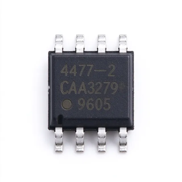
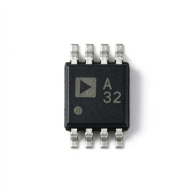
AD9873JS
AD9873JS - 232 MHz Mixed-Signal AFE | Analog Devices
The Analog Devices AD9873JS is a mixed-signal analog front-end converter with a complete 232 MHz quadrature digital transmitter, a 12-bit ADC, a 10-bit ADC, two 8-bit ADCs, and two sigma-delta control DACs, supplied in a 100-lead MQFP package. The device is designed for broadband communications, including cable set-top boxes, cable modems, and related video and digital-data systems.
A mixed-signal analog front-end, or AFE, combines analog signal acquisition and conversion functions with digital processing and interface functions on one integrated circuit. In the AD9873JS, this integration includes multiple ADC channels and a quadrature digital up-converter, allowing a system to receive and transmit broadband signals while limiting external component count. Its architecture is positioned for cost-sensitive broadband equipment where size, power dissipation, and dynamic performance are important.
The verified manufacturer material identifies a 232 MHz quadrature digital transmitter, output bandwidth up to 65 MHz, and a 12-bit TxDAC+ direct IF digital-to-analog converter. The receive section includes four ADCs with different resolutions: one 12-bit ADC, one 10-bit ADC, and two 8-bit ADCs. Two sigma-delta control DACs support control functions within the mixed-signal signal chain. The AD9873JS is identified as a 3.3 V CMOS analog front-end converter for MCNS-DOCSIS, DVB, and DAVIC-compliant set-top-box and cable-modem applications.
The AD9873JS combines a transmit path and multichannel receive path in one device, reducing the number of separate conversion and modulation blocks required by a broadband front end. The 232 MHz transmitter section is intended for quadrature digital signal generation, while the multichannel ADC section supports video and digital-data reception. This makes the device relevant to cable-modem headends, set-top-box receiver designs, DVB systems, and other broadband communication equipment requiring multiple conversion functions.
Typical implementation requires careful attention to analog input conditioning, clocking, digital data timing, power distribution, and PCB layout. Because the device integrates several high-speed and precision functions, decoupling and controlled return paths are essential for minimizing noise and crosstalk. The external interface and pin arrangement should be verified against the complete Analog Devices datasheet before PCB release, especially when matching the AD9873JS variant and its 100-lead MQFP footprint.
This page consolidates the verified AD9873JS product description, package identification, conversion features, application positioning, sourcing references, and design-oriented guidance. It also records where detailed electrical limits, timing values, pricing, pin assignments, and lifecycle information were not present in the supplied verified data, rather than inferring them.
詢價
聯絡我們