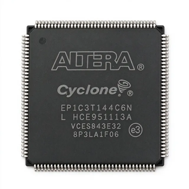
EP1C6F256I8N
EP1C6F256I8N - Cyclone FPGA, 6K LE, 256-BGA | Intel (Altera)
The Intel (formerly Altera) EP1C6F256I8N is a member of the first-generation Cyclone FPGA family, delivering 5,980 logic elements, 92,160 RAM bits, and 185 user I/O pins in a 256-ball FineLine BGA package, with an industrial temperature grade (I8N suffix denoting -40C to +100C operating range). Built on a 0.13-um SRAM-based process, the Cyclone EP1C6 is a low-cost programmable logic device that targets high-volume, cost-sensitive designs where ASIC-class integration is not economical.
A field programmable gate array (FPGA) is a semiconductor integrated circuit composed of configurable logic blocks (CLBs), programmable interconnect, and dedicated I/O elements that an engineer can program after manufacture to implement arbitrary digital logic. Within the broader integrated circuit hierarchy, FPGAs sit between fixed-function ASICs (high NRE, low unit cost at scale) and discrete logic/microcontrollers (flexible software, but limited by fixed hardware). The Cyclone family specifically occupies the low-density, low-cost tier of Altera/Intel's FPGA portfolio, designed for glue logic, bus bridging, DSP pre/post-processing, and parallel I/O expansion.
The EP1C6F256I8N integrates 5,980 logic elements (LEs), 92,160 bits of embedded RAM (M4K blocks), two PLLs, and supports up to 185 LVTTL/LVCMOS/LVDS/SSTL user I/Os. Configuration is via passive serial (PS), active serial (AS), or JTAG modes, supporting Altera EPCS1/EPCS4/EPCS16 serial configuration devices. The 256-ball FineLine BGA provides high pin density at manageable PCB routing complexity, making it suitable for space-constrained industrial, communications, and consumer designs.
Architecturally, the Cyclone EP1C6 employs a 4-input look-up-table (LUT) based LE with dedicated carry chain for arithmetic, distributed and block RAM for memory, and per-pin tri-state buffers for bus-oriented interfacing. The device supports LVDS signaling at up to 640 Mbps, DDR SDRAM interfaces with dedicated DQS strobe circuitry, and integrated multipliers for DSP operations. Two PLLs provide clock multiplication, division, phase shifting, and duty-cycle correction for system clock management.
Typical applications include industrial control and factory automation backplanes, telecommunications line cards and protocol bridging, video processing front-ends, motor control and drive interfaces, and consumer electronics requiring parallel DSP pipelines. Designers also choose the EP1C6 for legacy design maintenance, cost-sensitive retrofits, and as a flexible replacement for multiple discrete logic ICs on a single board.
When designing with the EP1C6F256I8N, careful attention must be paid to power sequencing (VCCINT before VCCIO), JTAG chain integrity for in-system programming, and thermal management in enclosed housings. For new designs, designers should evaluate the Cyclone IV E family as the modern, low-power successor; the EP1C6 remains in service for legacy platforms and long-life industrial deployments.
詢價
聯絡我們