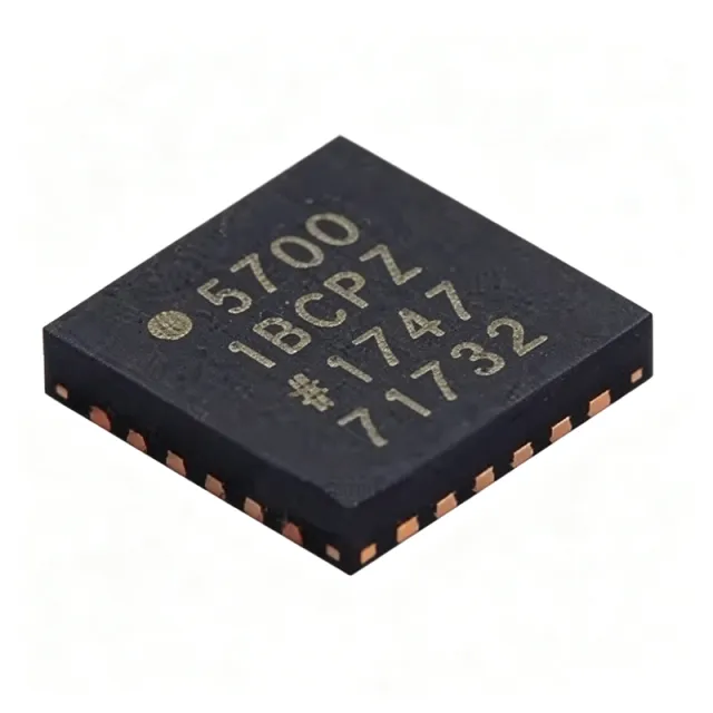
AD571KD/+
AD571KD/+ - 10-Bit SAR ADC in 18-Pin DIP | Analog Devices
Analog Devices AD571KD/+ is a 10-bit successive-approximation analog-to-digital converter housed in an 18-pin ceramic dual in-line package. The converter integrates a digital-to-analog converter, voltage reference, clock, comparator, successive-approximation register, and output buffers on one monolithic chip. Its primary characteristics are 10-bit resolution, commercial temperature grade, through-hole construction, and an 18-terminal rectangular DIP package.
An ADC is an interface component that converts an analog voltage into a digital number for processing, measurement, display, or control. The AD571 belongs to the successive-approximation, or SAR, ADC family. In this architecture, an internal DAC generates successive trial voltages, the comparator evaluates each trial against the input, and the successive-approximation register records the conversion result. The AD571 integrates the supporting conversion elements on one chip, reducing the number of external components required for a complete conversion channel.
The AD571's 10-bit conversion resolution provides 1,024 distinguishable digital codes across the converter's analog input range. This resolution is suitable for instrumentation and control systems that need moderate rather than high-resolution digital measurement. Its integrated reference, clock, comparator, DAC, register, and output buffers establish a self-contained conversion architecture, while the parallel output interface provides direct access to the converted code.
The AD571KD/+ is identified as a commercial-grade, through-hole device in an 18-pin SBCDIP package. The ceramic DIP construction and through-hole lead format suit legacy industrial, instrumentation, test, and control equipment where plated-through-hole assembly and direct socket or PCB mounting are preferred. The package also provides a straightforward mechanical format for repair and replacement of older embedded analog-measurement systems.
Typical applications include process-control instrumentation, digital panel meters, laboratory measurement equipment, sensor-interface circuits, industrial data-acquisition systems, and embedded control systems. In these systems, the AD571 can digitize a conditioned analog sensor signal while its integrated reference and conversion clock reduce the external support circuitry needed. System designers should still provide input conditioning, suitable bypassing, acquisition timing, and output-interface buffering.
For a new design, verify the required analog input range, conversion timing, output logic levels, reference behavior, and acquisition architecture against the manufacturer datasheet before allocating the PCB footprint. When upgrading an existing board, confirm that the 18-pin pinout and signal functions match, and account for the DIP package's larger footprint compared with modern surface-mount ADC packages.
This product page combines the AD571KD/+ device identity, package and converter architecture with replacement guidance, application-focused design guidance, and a parameter-by-parameter comparison. It is intended to help engineers identify the correct legacy-compatible ADC without confusing package variants, temperature grades, or functional alternatives with exact drop-in replacements.
詢價
聯絡我們