產品(46,000+)

M30624FGPFP#U5C - M16C/62P 16-bit MCU, 256KB Flash, 100-QFP | Renesas
M30624FGPFP#U5C

M30624FGPFP#U5C - M16C/62P 16-bit MCU, 256KB Flash, 100-QFP | Renesas

The Renesas Electronics M30624FGPFP#U5C is a single-chip 16-bit CMOS microcomputer from the M16C/60 Series M16C/62P Group, integrating 256 KB of flash memory and 24 MHz of CPU performance in a 100-pin QFP (14x20 mm) package. It combines the high-performance M16C/60 CPU core with the silicon-gate CMOS process, delivering 16-bit processing at low power consumption for embedded control applications. A microcontroller (MCU) is an integrated circuit that combines a CPU, memory (RAM/ROM/Flash), and programmable I/O peripherals on a single silicon die. The M16C family sits within the 16-bit microcontroller taxonomy, between 8-bit MCUs (e.g., 8051) and 32-bit ARM Cortex-M devices, offering a balance of code density, deterministic interrupt latency, and peripheral integration well suited to real-time control. The M16C/62P Group sits under the M16C/60 Series umbrella of Renesas's mid-range MCU portfolio. Key features include 256 KB of on-chip flash (256K x 8), 4 KB of on-chip RAM, a 24 MHz maximum CPU clock, a 10-bit A/D converter, a wide operating voltage range of 2.7V to 5.5V, and an operating temperature range of -20C to +85C. The 100-QFP package provides ample I/O for motor control, automotive body electronics, and industrial automation. Multiple timers, serial interfaces (UART, I2C, SPI), and interrupt controllers are integrated, eliminating the need for external peripherals. The M16C/60 CPU core uses a register-based architecture with 24-bit linear addressing, supporting high-level language efficiency and rich addressing modes. Built-in flash allows in-application reprogramming via serial or background programming modes, simplifying field firmware updates. The silicon-gate CMOS process yields low quiescent current and supports 3V and 5V system designs with a single part number. Typical applications include industrial motor control, HVAC control boards, automotive body ECUs, home appliance controllers (washing machines, microwave ovens), and metering/pump controllers. The wide 2.7V-5.5V supply range makes it suitable for both 3.3V and 5V logic designs. When designing with this MCU, ensure the 100-pin QFP footprint matches your PCB land pattern and provide adequate decoupling (100 nF + 10 uF) near each power pin. Use the on-chip debug/flash programming interface for production firmware loading rather than relying on external programmers. Note that Renesas recommends the newer M3062LFGPFP for new designs. This page consolidates distributor pricing, drop-in alternative analysis, and practical design notes beyond what the manufacturer datasheet alone provides.

詢價 聯絡我們
M30626FHPFP - 16-Bit 24MHz M16C/62P MCU, 384KB Flash | Renesas
M30626FHPFP

M30626FHPFP - 16-Bit 24MHz M16C/62P MCU, 384KB Flash | Renesas

The Renesas M30626FHPFP is a 16-bit single-chip CMOS microcontroller from the M16C/62P family, built around the high-performance M16C/60 Series CPU core with 384KB of on-chip flash memory and 24MHz maximum operating frequency, housed in a 100-pin QFP (14x20 mm) package. It supports 5V operation with a wide 2.7V to 5.5V supply range, integrates 31KB of RAM, and provides rich on-chip peripherals including multi-channel 10-bit A/D converter, DMA controller, three UART/SIO channels, and timers. An M16C/62P microcontroller is a 16-bit CISC MCU from the M16C family of single-chip microcomputers, engineered using high-performance silicon-gate CMOS process technology. It sits within the broader taxonomy of microcontroller -> embedded processor -> semiconductor IC, and is designed for industrial-grade control applications requiring deterministic real-time response, low EMI, and a robust instruction set optimized for C compiler code density. Key differentiating features include 384KB flash program memory (384K x 8 organization), 31KB RAM, 87 I/O pins, four DMA channels, three serial I/O blocks, 8-bit and 16-bit timers, a 10-bit A/D converter with up to 26 input channels, and a watchdog timer. It supports both 3V and 5V operation (industrial temperature range -40C to +85C) and is Pb-free, RoHS-compliant. The device implements the M16C/60 CPU core with 16-bit fixed instruction width, register-based architecture with 32KB address space, and efficient C-language support. Its integrated peripherals include CRC calculation hardware, intelligent I/O ports capable of key input wake-up, and a power-saving mode with multiple clock gearing options. The architecture enables deterministic interrupt latency for real-time control. Typical applications include industrial automation controllers, motor control inverters, factory automation PLCs, building HVAC controls, security system panels, vending machine controllers, and white goods control boards. The wide operating voltage (2.7V-5.5V) and industrial temperature range (-40C to +85C) make it suited to harsh environments. Design consideration: when migrating from earlier M16C/62 to M16C/62P, verify the watchdog timer and A/D converter channel mapping. Place a 0.1uF decoupling capacitor adjacent to each VCC/AVCC pin pair and keep the analog reference traces short to minimize digital switching noise on ADC sampling accuracy. This page synthesizes distributor pricing from DigiKey/Mouser, drop-in alternatives in the same 100-QFP package, and practical design notes that complement the manufacturer datasheet with field-application guidance.

詢價 聯絡我們
M30855FJGP#U3 - 16/32-Bit M32C/85 MCU, 512KB Flash, 144-LQFP | Renesas
M30855FJGP#U3

M30855FJGP#U3 - 16/32-Bit M32C/85 MCU, 512KB Flash, 144-LQFP | Renesas

The Renesas M30855FJGP#U3 is a 16/32-bit single-chip CMOS microcontroller from the M32C/80 series (M32C/85 group) operating at up to 32 MHz, integrating 512 KB of on-chip flash program memory and 24 KB of RAM in a 144-pin LFQFP (20x20 mm) package. The part is specified over an industrial temperature range of -40C to +85C and operates from a 3 V to 5.5 V supply, making it compatible with both 3.3 V and 5 V system designs. The M30855FJGP#U3 offers 121 general-purpose I/O pins, multiple on-chip peripherals including timers, serial interfaces (UART/SIO/I2C), an A/D converter, and DMA channels for high-throughput embedded control. A microcontroller (MCU) is a self-contained computing subsystem that integrates a CPU core, program and data memory, peripherals, and I/O on a single silicon die. Within the broader semiconductor taxonomy, MCUs belong to the integrated circuits family, specifically the microcontroller subcategory, and sit below microprocessors in complexity while providing complete embedded-control functionality. The M32C/80 platform is Renesas' legacy 16-bit CISC architecture with 32-bit internal registers, popular in industrial automation, automotive body controllers, and consumer appliances. Key features of the M30855FJGP#U3 include 512 KB flash program memory (512K x 8), 24 KB of RAM (24K x 8), a maximum operating frequency of 32 MHz, an internal oscillator, and 121 user I/O pins routed through the 144-LFQFP package. The wide 3 V to 5.5 V supply range simplifies integration into both legacy 5 V designs and modern 3.3 V subsystems without level shifters, while the industrial temperature grade enables deployment in factory, automotive cabin, and outdoor equipment. The M32C/85 core architecture uses a CISC instruction set optimized for compact code density, with hardware multipliers, multiple register banks, and a rich interrupt controller that supports real-time control loops. The integrated DMA reduces CPU load for high-speed peripheral transactions such as serial communication and A/D conversion. Typical applications for the M30855FJGP#U3 include industrial factory automation systems, automotive body electronics, consumer appliance control boards, and general-purpose 16-bit embedded platforms. Engineers select this part for designs that require a mature, well-supported Renesas M16C/M32C software ecosystem. When designing with the M30855FJGP#U3, ensure that the chosen emulator/debugger (such as the E8a or E10A-USB) matches the device group, and follow the M32C/85 hardware manual pin-function assignment tables to avoid peripheral conflicts on the 121 I/O pins. This page synthesizes verified distributor pricing, drop-in alternative MPNs from the Renesas M16C/M32C family, and practical design notes not consolidated on any single manufacturer page.

詢價 聯絡我們
M321R4GA0PB2-CCP - 32GB DDR5-6400 ECC RDIMM | Samsung
M321R4GA0PB2-CCP

M321R4GA0PB2-CCP - 32GB DDR5-6400 ECC RDIMM | Samsung

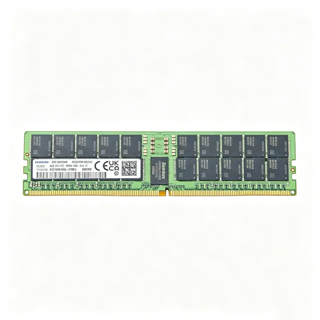
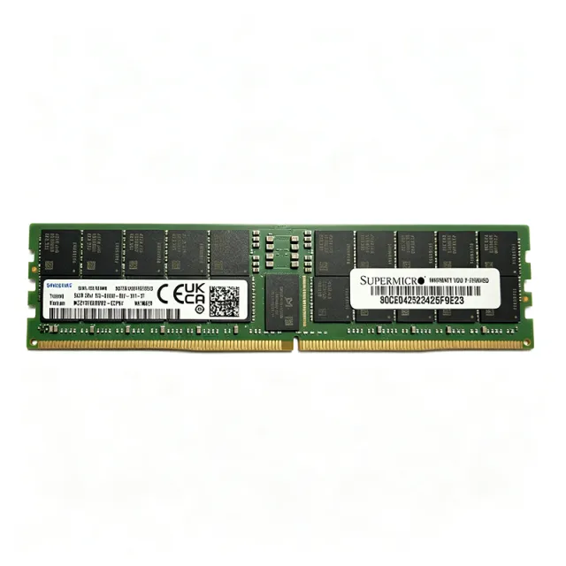
The Samsung M321R4GA0PB2-CCP is a 32GB DDR5-6400 ECC registered DIMM (RDIMM) operating at 6400 MT/s (PC5-51200) on a 1.1V supply, packaged as a 288-pin DIMM in a 1Rx4 single-rank x4 configuration. A registered DIMM (RDIMM) is a server memory module that buffers the address and command signals through a register chip before they reach the DRAM devices. This buffering reduces the electrical load on the memory controller, enabling higher module counts per channel and greater total capacity in servers and workstations. RDIMMs sit within the DDR5 SDRAM module hierarchy: DRAM device -> FBGA-packaged die -> registered DIMM -> memory subsystem, and they differ from LRDIMMs (which buffer data as well) and UDIMMs (which have no buffering). Key features of the M321R4GA0PB2-CCP include 32GB capacity organized as 4G x 72 (including 8 bits of ECC per 64-bit word), DDR5-6400 operation at CL52 latency, on-die ECC plus side-band ECC checking, and 1.1V operation aligned with the JEDEC DDR5 standard for reduced power per bit versus DDR4. The module uses twenty 4G x 4 DDR5 DRAM devices in FBGA packages, giving a single-rank x4 topology that the memory controller addresses as one rank. Technically, DDR5 moves the power management from the motherboard to an on-module PMIC (12V to 1.1V conversion), improving signal integrity and power efficiency. Dual 32-bit sub-channels per module improve effective bandwidth and reduce contention. The -CCP speed bin denotes the 6400 MT/s grade, delivering 51.2 GB/s peak bandwidth per channel pair. Typical applications include enterprise servers, edge compute nodes, low virtual-machine-density hosts, workstations, and general-purpose data center platforms from Dell PowerEdge, HPE ProLiant, Lenovo ThinkSystem, and Supermicro using Intel Xeon or AMD EPYC processors with DDR5 memory controllers. A key design consideration: RDIMMs must only be mixed with other RDIMMs of the same generation on a channel; they cannot be combined with UDIMMs or LRDIMMs, and maximum supported speed depends on the CPU memory controller and populated channel configuration. This page synthesizes distributor pricing and availability data, JEDEC-compliant drop-in alternatives from multiple vendors, and practical deployment notes not consolidated in the manufacturer documentation.

詢價 聯絡我們
M321R4GA3EB0-CWM - 32GB DDR5-5600 ECC RDIMM | Samsung
M321R4GA3EB0-CWM

M321R4GA3EB0-CWM - 32GB DDR5-5600 ECC RDIMM | Samsung

The Samsung M321R4GA3EB0-CWM is a 32GB DDR5-5600 ECC Registered DIMM (RDIMM) operating at 1.1V with CL46 latency, housed in a 288-pin DIMM form factor. This dual-rank x8 (2Rx8) module delivers PC5-44800 bandwidth and is organized as 4Gx72 with twenty FBGA-packaged 2Gx8 DDR5 DRAM devices plus a registering clock driver for server-grade reliability. A Registered DIMM (RDIMM) is a server memory module that buffers address and command signals through a registering clock driver (RCD), reducing electrical load on the memory controller and enabling higher capacities and densities than unbuffered UDIMMs. RDIMMs sit within the DDR5 SDRAM family, which itself belongs to the broader category of volatile DRAM memory used in servers, workstations, and enterprise storage. ECC (Error Correcting Code) functionality detects and corrects single-bit memory errors, which is essential for data integrity in 24/7 datacenter operation. Key features include DDR5-5600 data rate (PC5-44800), 32GB capacity in a dual-rank configuration that balances density and signal integrity, 1.1V operation that lowers power draw versus DDR4's 1.2V, and on-module ECC registered architecture. DDR5's on-die ECC, bank grouping, and dual 32-bit subchannels per DIMM improve effective bandwidth and reliability at speed. Technically, the module uses 20 pieces of 2Gx8 FBGA DDR5 DRAM across two ranks, with a registering clock driver managing command/address traffic. The x72-wide data path (64-bit data plus 8 bits of ECC-style check bandwidth) supports the RDIMM error-handling architecture. Typical applications include Dell PowerEdge C6620, MX760c, R660, and R660xs servers (OEM cross-reference Dell P8XPW), edge compute nodes, low-VM-density hosts, and general-purpose virtualization platforms that list DDR5-5600 RDIMMs on their qualified vendor list. Design consideration: always verify module presence against the server platform's Qualified Vendor List (QVL), since RDIMM speed may train down if the platform only supports lower DDR5 rates. This page synthesizes distributor pricing, drop-in alternatives, and platform compatibility data not consolidated in the manufacturer datasheet.

詢價 聯絡我們
M321R8GA0EB2-CWM - 64GB DDR5-5600 ECC RDIMM | Samsung
M321R8GA0EB2-CWM

M321R8GA0EB2-CWM - 64GB DDR5-5600 ECC RDIMM | Samsung

The Samsung M321R8GA0EB2-CWM is a 64GB DDR5-5600 ECC registered DIMM (RDIMM) with dual-rank x4 (2Rx4) organization, operating at 1.1V on a 288-pin DIMM module built with Samsung D-die DRAM devices in a (4G x 4) x 40 composition. Registered (buffered) DIMMs are a class of server memory modules in which address, command, and control signals pass through a register chip before reaching the DRAM devices. This buffering reduces the electrical load on the memory controller, allowing servers and workstations to populate more DIMM slots per channel than is possible with unbuffered (UDIMM) memory. RDIMMs sit within the memory module hierarchy: DDR5 SDRAM device -> registered DIMM -> server memory -> enterprise datacenter memory subsystem. On-die ECC plus registered operation makes them mandatory in most multi-socket x86 server platforms. Key features of the M321R8GA0EB2-CWM include 5600 MT/s data rate (2800 MHz clock, PC5-44800 bandwidth class), CAS latency of CL46 at the rated speed, dual-rank x4 organization that improves server memory capacity scaling, and 1.1V operation that lowers power draw versus DDR4 RDIMMs running at 1.2V. The DDR5 architecture also moves the power management IC (PMIC) onto the module and introduces two independent 32-bit subchannels per module, improving memory bandwidth efficiency for multi-core CPUs. Technically, the module uses Samsung D-die 4G x 4 DDR5 DRAM components, 40 of which compose the 64GB (8G x 72 including ECC bits) registered module. The x4 device width combined with registered operation supports strong RAS (reliability, availability, serviceability) characteristics demanded in virtualization and database environments. On-die ECC detects and corrects single-bit errors internal to each DRAM die, while the registered interface maintains signal integrity at high slot counts. Typical applications include Dell PowerEdge, HPE ProLiant, Lenovo ThinkSystem, and Supermicro server platforms, as well as virtualization hosts, in-memory databases, and AI inference servers requiring high-capacity registered memory. Multiple identical modules should be installed in matched sets for optimal multi-channel bandwidth. When designing or upgrading, confirm platform BIOS support for DDR5-5600 RDIMMs, as many platforms default to lower speeds such as 4800 MT/s or 5200 MT/s depending on populated DIMMs per channel. Mixing module speeds causes all modules to run at the slowest common speed. This page synthesizes verified distributor specifications, drop-in alternatives, pricing context, and practical deployment notes not consolidated in the manufacturer datasheet.

USD $2,826.92 聯絡我們
M321RYGA0PB2-CCP - 96GB DDR5-6400 ECC RDIMM | Samsung
M321RYGA0PB2-CCP

M321RYGA0PB2-CCP - 96GB DDR5-6400 ECC RDIMM | Samsung

The Samsung M321RYGA0PB2-CCP is a 96 GB DDR5-6400 ECC Registered DIMM (RDIMM) server memory module rated at 6400 MT/s (PC5-51200) with 1.1 V nominal operation, organized as 2Rx4 (dual-rank, x4 DRAM) in a 288-pin RDIMM form factor. It is built from 40 FBGA 6Gx4 DDR5 DRAM devices and delivers a 72-bit ECC data path (12GX72 organization) for enterprise servers and workstations. A Registered DIMM (RDIMM) is a server memory module that places a register (RCD) and data buffers between the DRAM devices and the memory controller, reducing electrical load on the command/address bus and enabling higher module densities and higher speeds than unbuffered DIMMs. Within the memory hierarchy, an RDIMM sits above UDIMM and SODIMM in capacity and reliability, and below LRDIMM in load reduction; it is the mainstream choice for two-socket and four-socket x86 servers. DDR5 adds on-module PMIC power management, on-die ECC, and two 32-bit subchannels per module. Key features of the M321RYGA0PB2-CCP include 96 GB capacity in a single module, 6400 MT/s transfer rate, 2Rx4 organization for maximum rank-level interleaving, ECC Registered operation for data integrity, and 1.1 V DDR5 standard voltage. The 96 GB density is achieved with non-binary 24 Gb DDR5 DRAM dies, allowing high capacity without the cost of 3DS stacking. Technically, the module uses 40 FBGA 6Gx4 DRAM packages arranged in two ranks of twenty devices each, with a 288-pin edge connector and a 72-bit ECC data path. The on-module PMIC and SPD hub are part of the JEDEC DDR5 RDIMM architecture, and the module is 100% JEDEC compliant per distributor documentation. Typical applications include enterprise rack servers, virtualization hosts, in-memory databases, and high-performance workstations where 96 GB per DIMM enables dense configurations. The 2Rx4 organization and ECC RDIMM design suit memory-bandwidth-bound workloads such as AI inference, analytics, and VDI. When designing or upgrading, verify that the server platform supports 24 Gb non-binary DDR5 DRAM and 96 GB RDIMM densities, and populate DIMMs per the vendor's population rules to maintain rated 6400 MT/s speed. This page synthesizes distributor pricing, drop-in alternatives, and practical design notes not found in the manufacturer datasheet.

USD $3,445.31 有庫存
M41T65Q6F - Serial RTC with Alarm, I2C, 1.3V-3.6V | STMicroelectronics
M41T65Q6F

M41T65Q6F - Serial RTC with Alarm, I2C, 1.3V-3.6V | STMicroelectronics

The STMicroelectronics M41T65Q6F is a serial access real-time clock (RTC) integrated circuit with alarm functions, providing a complete Clock/Calendar function plus 32.768 kHz output in a 16-pin VQFN exposed-pad package. The device communicates through a 400 kHz I2C (2-wire serial) interface, operates from 1.3 V to 3.6 V supply, and integrates memory-mapped registers for seconds, minutes, hours, day, date, month, year, and century tracking with automatic leap-year compensation through the year 2100. A Real-Time Clock (RTC) is a category of low-power timing IC that maintains accurate wall-clock time and date information independent of the system microcontroller. RTCs are essential components in any battery-backed system that must preserve time-of-day across power cycles. The M41T65 belongs to the RTC IC > Clock/Calendar > I2C RTC sub-family, and within ST's product hierarchy it sits under Timekeeping ICs > Serial RTC > RTC with Alarms. RTCs bridge the gap between digital logic and physical time by using a 32.768 kHz crystal oscillator as the time-base reference and counting oscillator cycles to derive seconds, minutes, hours, and calendar days. Key features of the M41T65Q6F include a wide operating voltage range of 1.3 V to 3.6 V (suitable for direct battery backup operation), integrated alarm and interrupt functions, a programmable square-wave output derived from the 32.768 kHz crystal, low power consumption typically below 1 microamp in battery backup mode, and an automatic backup switchover when VCC falls below a defined threshold. The 16-pin VQFN-EP (QFN-16) exposed-pad package provides low thermal resistance for stable operation across the -40 °C to +85 °C industrial temperature range and supports automated PCB assembly. Architecturally, the M41T65Q6F combines a 32.768 kHz crystal oscillator, frequency divider chain, BCD-coded time/date registers, I2C interface logic, alarm comparators, and a trickle charger circuit. The internal oscillator drives a divider that produces 1-second resolution. Time and date are stored in Binary-Coded Decimal (BCD) format for direct display compatibility. The integrated trickle charger allows the device to recharge an external backup supercapacitor or rechargeable battery when main power is present, then automatically switch over to backup supply on VCC failure. Typical applications include metering and data-logging systems, industrial controllers requiring time-stamped events, point-of-sale (POS) terminals, medical devices needing scheduled dosing or data recording, consumer electronics with calendar/alarm functions, and any battery-backed embedded system that needs to wake the host MCU at scheduled times. The low 1.3 V minimum supply also makes the M41T65Q6F well-suited for single-cell battery systems. When designing with the M41T65Q6F, ensure the 32.768 kHz crystal load capacitance matches the datasheet specification (typically 12.5 pF) and place the crystal traces as short and symmetric as possible to minimize parasitic capacitance. A decoupling capacitor of 0.1 microfarad should be placed within 2 mm of the VCC pin. The exposed pad (EP) must be soldered to the ground plane for mechanical and thermal reliability. This page synthesizes distributor pricing, package-equivalent alternatives in the same ST M41Txx RTC family, and practical design notes not aggregated on the manufacturer datasheet PDF.

詢價 聯絡我們
M41T81SM6F - Serial RTC 2.7-5.5V I2C 8-SOIC | STMicroelectronics
M41T81SM6F

M41T81SM6F - Serial RTC 2.7-5.5V I2C 8-SOIC | STMicroelectronics

The STMicroelectronics M41T81SM6F is a low-power serial real-time clock (RTC) with a built-in 32.768 kHz external-crystal-controlled oscillator, supplied in an 8-pin SOIC (SO-8) surface-mount package. It operates from 2.7 V to 5.5 V, communicates over a 400 kHz I2C (2-wire) serial interface, and provides a 64-byte BCD-formatted clock/calendar register map covering tenths/hundredths of seconds through century. A Real-Time Clock (RTC) is a dedicated integrated circuit that keeps track of wall-clock time even when the main system is powered down. RTCs sit at the bottom of the timekeeping hierarchy: RTC -> clock/calendar IC -> clock and timing -> semiconductor. They are essential wherever a system must maintain accurate time/date stamping across power cycles, such as data loggers, metering equipment, and industrial controllers. The M41T81S is one of the few RTCs that integrates both the 32.768 kHz crystal interface and the compensation circuitry in a single 8-pin package, reducing BOM and board area. Key features include 2.7 V to 5.5 V single-supply operation, low typical current consumption for battery-backed operation, programmable alarm and watchdog functions, automatic leap-year compensation through year 2099, and a software clock calibration function that can compensate crystal aging in 5 ppm steps. The I2C slave address is fixed at 0x68 with the A0 pin grounded. Internally, the M41T81S combines an external 32.768 kHz crystal oscillator circuit with a binary-coded decimal (BCD) counter chain. Eight bytes of on-chip SRAM back the clock/calendar registers and are accessed via the standard I2C protocol. The device supports both 100 kHz Standard-mode and 400 kHz Fast-mode I2C, making it compatible with most microcontroller families. The byte-wide register map follows the ST M41Txx family convention for drop-in software portability. Typical applications include industrial automation controllers, point-of-sale terminals, metering (electricity/water/gas), data loggers, medical devices requiring timestamped events, automotive telematics and infotainment subsystems, security and access-control panels, and any battery-backed embedded system needing persistent wall-clock time. When designing with the M41T81SM6F, place the 32.768 kHz crystal within 5 mm of the OSCIN/OSCOUT pins and guard those traces with a ground ring to minimize stray capacitance. Provide a backup battery (typically a 3 V coin cell) on VCC with a series Schottky or Schottky-plus-resistor OR-ing network so the RTC domain remains powered during main-rail outages. Use 100 nF decoupling close to VCC and observe the I2C pull-up sizing rules for the chosen bus speed. This page consolidates distributor pricing, parametric drop-in alternatives, and practical layout notes that complement the manufacturer datasheet, giving engineers a single reference for sourcing and designing in the M41T81SM6F.

詢價 聯絡我們
M41T82RM6F - Low-Power I2C RTC with 32.768 kHz | STMicroelectronics
M41T82RM6F

M41T82RM6F - Low-Power I2C RTC with 32.768 kHz | STMicroelectronics

The STMicroelectronics M41T82RM6F is a low-power serial I2C real-time clock and calendar with a built-in 32.768 kHz oscillator, a 7-bit register address format, and an 8-pin SOIC package measuring 3.90 mm wide. It operates from a 2.0 V to 5.5 V clock supply range and provides battery-backed timekeeping with an ultra-low battery supply current of 365 nA. The device is designed for systems that require accurate calendar time, programmable alarms, periodic events, and low standby power. A real-time clock is a specialized timekeeping integrated circuit that maintains seconds, minutes, hours, date, day, month, and year information even when the main system is unpowered. The RTC category sits within clock and timing semiconductors, where crystal-based oscillators, dividers, registers, and digital interfaces work together to provide a stable time reference. Unlike a software timer, an RTC can continue counting through power loss and can be read again when the host processor restarts. The M41T82RM6F combines an external-crystal-controlled oscillator architecture with low-power serial communication. Its programmable alarm and timer functions can wake a connected microcontroller or signal that a scheduled interval has elapsed. The I2C interface reduces wiring requirements in compact embedded systems, while the 2.0 V to 5.5 V operating range supports both low-voltage and conventional supply environments. The 365 nA battery supply current is especially relevant for battery-backed meters, industrial recorders, and portable instruments. The STMicroelectronics M41T82 family description identifies the SO8 version as using an external 32.768 kHz crystal. Accurate timekeeping therefore depends not only on the RTC electronics but also on crystal selection, load-capacitance matching, layout quality, and temperature behavior. The M41T82RM6F is suited to data loggers, access-control terminals, metering equipment, industrial controllers, and consumer products requiring persistent timestamps. Its low standby consumption helps reduce energy use when the main supply is absent. For a robust design, place the RTC and its crystal close together on the PCB, keep high-current switching paths away from the oscillator network, and provide the required bypass capacitance. Confirm the exact pin functions, register behavior, alarm polarity, and electrical limits against the manufacturer datasheet before layout release. The verified source data supports the component identity, package, interface, oscillator, supply range, and low-current claims; additional operating details remain subject to the full STMicroelectronics datasheet. This page combines verified manufacturer and distributor information with application guidance, comparison fields, and design notes. It is intended to help engineers identify whether the M41T82RM6F fits a low-power battery-backed timekeeping design while distinguishing verified facts from parameters requiring confirmation from the latest datasheet.

詢價 聯絡我們
M41T94MQ6F - Serial RTC 44B NVRAM SPI 16-SOIC | STMicroelectronics
M41T94MQ6F

M41T94MQ6F - Serial RTC 44B NVRAM SPI 16-SOIC | STMicroelectronics

The STMicroelectronics M41T94MQ6F is a serial real-time clock (RTC) with 44 bytes of NVRAM and a RESET output, packaged in a 16-pin SOIC (0.154", 3.90 mm width). It provides a complete clock/calendar function with tenths/hundredths of seconds, seconds, minutes, hours, day, date, month, year, and century counters, and communicates with the host MCU through a 4-wire SPI bus at clock rates up to 2 MHz. The internal 32,768 Hz oscillator integrates 12.5 pF of load capacitance, allowing direct connection of an external tuning fork crystal without external load capacitors while still tolerating high crystal series resistance (up to 80 kΩ typical). A real-time clock (RTC) is a low-power integrated circuit that maintains accurate wall-clock time using a quartz crystal reference, even when the main system is powered down. RTCs sit within the broader hierarchy of clock-and-timing ICs, which include general-purpose timers, oscillators, and PLL/clock generators. Unlike MCU-internal time counters, dedicated RTC ICs add battery backup switchover, calendar logic, and non-volatile user memory that survives both system reset and loss of main supply. Key features of the M41T94MQ6F include SPI serial interface, 44 bytes of battery-backed NVRAM (16 bytes general-purpose plus 8 bytes used by the clock/calendar), a RESET output pin that asserts a fixed-duration low pulse for system brown-out management, and an integrated 32 kHz oscillator with on-chip load capacitance. The device operates from 2.7 V to 5.5 V main supply and is specified for the industrial -40 °C to +85 °C temperature range. Typical applications include metering (electricity/water/gas), point-of-sale terminals, data loggers, industrial controllers, and any embedded system that needs a tamper-resistant, battery-backed time stamp separate from the application MCU. Designers should add a lithium backup cell (or supercapacitor) to the VBAT pin and follow the crystal-layout guidance in the ST datasheet for long-term timekeeping accuracy.

詢價 聯絡我們
M471A2G43AB2-CWE - 16GB DDR4-3200 SO-DIMM | Samsung
M471A2G43AB2-CWE

M471A2G43AB2-CWE - 16GB DDR4-3200 SO-DIMM | Samsung

The Samsung M471A2G43AB2-CWE is a 16 GB unbuffered non-ECC DDR4 SO-DIMM module rated at 3200 MT/s (PC4-25600), organised as a single 1x16 GB rank in the industry-standard 260-pin SO-DIMM form factor used in laptops, mini-PCs, and small-form-factor systems. A SO-DIMM (Small Outline Dual In-Memory Module) is a compact JEDEC-standard memory module derived from the full-size DIMM but roughly half the height. DDR4 SDRAM is the fourth generation of double data rate synchronous DRAM; it operates at lower voltage (1.2 V) than DDR3 (1.5 V), reaches higher per-pin data rates up to 3200 MT/s at launch, and uses a 288/260-pin edge connector with point-to-point topology. The SO-DIMM variant mounts vertically in laptop sockets and supports up to 2 ranks per module (2DPC in some platforms). Key features include 16 GB density in a 1Rx8 organisation (built from sixteen 1 Gx8 FBGA-78 die), 3200 MT/s transfer rate (PC4-25600), CAS Latency 22 (CL22), 1.2 V typical operating voltage (1.14-1.26 V per JEDEC DDR4 spec), and JEDEC-compliant 260-pin SO-DIMM edge finger geometry. The module is unbuffered, non-ECC, and supports standard SPD timings for plug-and-play compatibility with Intel and AMD mobile platforms. Technically, the module follows the JEDEC DDR4 standard JESD79-4, supporting on-die termination (ODT), command/address parity on qualified platforms, and write CRC for signal-integrity robustness. The 1Rx8 organisation routes a single 64-bit data word through eight x8 DRAM devices per rank, balancing density and signal loading for mobile workloads. Typical applications include laptop memory upgrades, ultrabook and thin-client RAM expansion, mini-PC and small-form-factor workstations, and embedded industrial PCs that require JEDEC-standard SO-DIMM compatibility. The 3200 MT/s rating aligns with mainstream 11th/12th-generation Intel Core and AMD Ryzen mobile platforms. Design consideration: when populating two SO-DIMM sockets, mixing 1Rx8 and 2Rx8 modules downgrades the channel to the slower rank's timings on some chipsets - use matched modules for dual-channel performance. This page synthesises distributor pricing, JEDEC-aligned specifications, drop-in alternatives, and practical upgrade notes not always shown on a single distributor listing.

詢價 聯絡我們
M48T02-70PC1 - 5V 16Kbit TimeKeeper SRAM RTC | STMicroelectronics
M48T02-70PC1

M48T02-70PC1 - 5V 16Kbit TimeKeeper SRAM RTC | STMicroelectronics

The STMicroelectronics M48T02-70PC1 is a 5.0 V, 16 Kbit (2 Kb x 8) non-volatile TimeKeeper SRAM that integrates an ultra-low-power SRAM, a real-time clock (RTC), and a power-fail control circuit in a single 24-pin DIP Module package (0.600 inch / 15.24 mm). The device is pin and function compatible with the JEDEC-standard 2 Kb x 8 SRAM footprint, allowing direct replacement of a parallel SRAM while adding battery-backed timekeeping. Access time is 70 ns, matching common asynchronous SRAM timing requirements. The on-board lithium coin cell provides a minimum of 10 years of data and clock retention in the absence of external power across the operating temperature range. A real-time clock (RTC) is a dedicated integrated circuit that tracks seconds, minutes, hours, days, dates, months, and years with automatic leap-year compensation. The M48T02 family combines RTC functionality with a non-volatile static RAM, forming a TIMEKEEPER (utility) hybrid module that retains data and time without external backup hardware. Such modules sit in the system hierarchy as Memory ICs > Non-volatile SRAM > RTC + SRAM combination modules, and are widely used when a host MCU needs both configuration storage and wall-clock time across power cycles. Key features include a parallel address/data bus interface (multiplexed to match a standard 2K x 8 SRAM pinout), BCD-formatted clock registers, automatic leap-year correction through 2099, programmable square-wave output, and built-in power-fail write protection that locks the SRAM when VCC drops below the lithium backup threshold. The TIMEKEEPER (utility) architecture means the user simply reads and writes the SRAM address space - clock information is mapped into the upper RAM addresses - so existing SRAM software drivers work with no modification. Typical applications include industrial controllers, point-of-sale terminals, data loggers, metering equipment, security and access-control systems, and any embedded design that needs both battery-backed parameter memory and a calendar-clock. Designers should observe the VCC power-up ramp specifications in the datasheet to ensure the battery switchover circuit latches correctly, and avoid applying external bias to the backup cell. The through-hole DIP-24 module remains popular for legacy boards, prototypes, and field-replaceable designs where socketed parts are desirable.

詢價 聯絡我們
M48T58-70PC1 - 64Kbit Timekeeper SRAM RTC 70ns | STMicroelectronics
M48T58-70PC1

M48T58-70PC1 - 64Kbit Timekeeper SRAM RTC 70ns | STMicroelectronics

The STMicroelectronics M48T58-70PC1 is a 5.0 V, 64 Kbit (8 Kb x 8) non-volatile Timekeeper SRAM that integrates an 8 Kb x 8 static RAM, a real-time clock, a power-fail control circuit, and a lithium battery in a single 28-pin DIP Module package. It provides 70 ns access time and operates over a 4.75 V to 5.5 V supply range, delivering a battery-backed-up memory and real-time clock solution in one footprint. A Timekeeper SRAM is a hybrid non-volatile memory device that combines the byte-wide random access of a standard SRAM with on-chip battery backup and an integrated real-time clock. It belongs to the broader family of non-volatile RAM (NVRAM) products, sitting between conventional SRAM and serial NVSRAM/FRAM in the memory hierarchy. Compared to standard SRAM, a Timekeeper eliminates external battery-management circuitry and supports BCD-coded year/month/day/date/hour/minute/second read-out. Key features include 70 ns read/write access time, integrated lithium battery with typical 10-year data retention, automatic power-fail/write-protection circuitry, bytewide RAM-like clock access, BCD-coded year/month/day/date/hour/minute/seconds registers, frequency test output for real-time clock, and JEDEC-standard 8 K x 8 SRAM pin/function equivalence. The monolithic chip ships in a special 28-pin DIP Module (CAPHAT) that accommodates the embedded battery cell. The architecture centers on a low-power 8K x 8 SRAM array, a 32 kHz crystal-controlled oscillator for the RTC, and a power-fail comparator that latches the CS/WE/OE write-protect signals when VCC drops below a defined threshold. The internal lithium cell then holds both the SRAM contents and the RTC registers, allowing the device to drop into any JEDEC-standard 8K x 8 SRAM socket without any WRITE-timing constraints. Typical applications include industrial data logging, point-of-sale terminals, metering equipment, factory automation controllers, medical instruments, and any embedded system that requires both non-volatile variables and a wall-clock/calendar without an external backup battery or RTC chip. Designers use it as a one-chip substitute for SRAM + discrete RTC + supercapacitor/cell combinations. When designing with this device, observe the standard 8K x 8 SRAM timing (address setup, CS-to-OE, write-pulse width) and route the VCC decoupling close to the supply pin. Because the lithium cell is non-replaceable in the CAPHAT package, treat the module as a sealed unit; planned end-of-life data retention after VCC removal is on the order of 10 years per the manufacturer. This page synthesizes distributor pricing, verified drop-in alternatives, and practical design notes that go beyond the manufacturer's datasheet, supporting faster component evaluation.

詢價 聯絡我們
M4A5-64/32-7JI - ispMACH 4A 64-Macrocell 5V CPLD | Lattice
M4A5-64/32-7JI

M4A5-64/32-7JI - ispMACH 4A 64-Macrocell 5V CPLD | Lattice

The Lattice Semiconductor M4A5-64/32-7JI is a 64-macrocell, 32-user-I/O member of the ispMACH 4A family of high-performance E2CMOS 5-V in-system programmable complex programmable logic devices (CPLDs), supplied in a 44-pin Plastic Leaded Chip Carrier (PLCC) package with surface-mount J-leads. It offers 2.5K usable gates, 7.5 ns typical propagation delay (tpd), and an internal operating frequency up to 125 MHz, making it one of the fastest 5-V CPLDs of its generation. A CPLD (Complex Programmable Logic Device) is a non-volatile programmable logic device that combines multiple PAL/GAL-style macrocell blocks with a central interconnect matrix, providing deterministic, single-clock-cycle logic with predictable timing. CPLDs sit below FPGAs in the programmable logic hierarchy: they offer fewer gates than FPGAs but provide instant-on operation, superior pin-to-pin timing consistency, and robust 5-V I/O tolerance, which is why they remain preferred for glue logic, bus interfacing, and power-sequencing tasks. Key features include 100% pin-out retention, 100% macrocell utilization, in-system programmability via IEEE 1532 / JTAG, four 36-input PAL blocks with 16 macrocells each, and a global routing pool that delivers fast, predictable signal propagation. The 5-V tolerant I/Os simplify interfacing to legacy TTL/CMOS buses without level shifters. The ispMACH 4A architecture uses Lattice's E2CMOS process with non-volatile storage of the configuration, so the device powers up in a known functional state with no external boot PROM. The four-block, single-pool interconnect fabric delivers uniform 7.5 ns pin-to-pin delays across all I/O combinations. Typical applications include address decoding and bus interfacing in 5-V industrial controllers, glue logic between microprocessors and peripherals, power-supply sequencing logic, and legacy system upgrades that require drop-in 5-V programmable logic with JTAG in-field reprogrammability. When designing with the M4A5-64/32-7JI, observe the 4.75 V to 5.25 V supply range and place 0.1 uF decoupling capacitors adjacent to every VCC pin. Because the part is in-system programmable, expose TDI, TDO, TMS, and TCK to a JTAG header for field updates. This page synthesizes distributor inventory, drop-in alternatives, and practical design notes for engineers migrating away from the obsolete original Lattice part number.

詢價 聯絡我們
M4T28-BR12SH1 - 48mAh SNAPHAT Lithium Battery + 32.768 kHz Crystal | STMicroelectronics
M4T28-BR12SH1

M4T28-BR12SH1 - 48mAh SNAPHAT Lithium Battery + 32.768 kHz Crystal | STMicroelectronics

The STMicroelectronics M4T28-BR12SH1 is a SNAPHAT® top battery-and-crystal module that delivers 48 mAh of lithium backup capacity at 2.8 V with an integrated 32.768 kHz quartz crystal (12.5 pF load), purpose-built as the detachable power source for ST's TIMEKEEPER® series of serial real-time clocks and non-volatile SRAM/Supervisor ICs housed in 28- and 44-pin surface-mount SOIC packages. The SNAPHAT design lets the lithium cell and crystal be snapped onto an SOIC base after reflow, keeping the battery off the board during high-temperature assembly and giving the end product years of battery-backed RTC retention. A lithium coin-cell backup battery is a primary (non-rechargeable) lithium cell that keeps volatile memory and real-time clock registers alive when the system main rail collapses; for non-volatile SRAM supervisors and RTCs it sits in the same supply hierarchy as a coin cell, a supercap-backed supply, and a buck/boost hold-up rail. In the TIMEKEEPER family the SNAPHAT module also carries the 32.768 kHz tuning-fork crystal so that the combined Battery+Crystal pair forms a complete timekeeping sub-assembly — the IC underneath just exposes a top-of-package cavity that the SNAPHAT clips into. Key features include a 48 mAh nominal capacity with lithium chemistry (long-shelf-life primary cell), an integrated 32.768 kHz crystal specified for 12.5 pF load capacitance, a typical operating voltage of 2.8 V and a detachable SNAPHAT housing that allows board-level assembly of the SOIC base before the lithium part is added. ST publishes a multi-year backup time figure and an estimated self-discharge shelf life at +25 °C so the engineer can size RTC retention against product life. Inside the SNAPHAT housing, the lithium coin cell is connected through the SOIC pinout's Vbat/RET pins while the crystal ties to the RTC's oscillator pins; the SNAPHAT body itself provides the mechanical alignment and the battery contact springs. Because the same SNAPHAT accepts both M4T28-BR12SH1 and M4T32-BR12SH1 variants, the top is reusable across ST's 28- and 44-pin TIMEKEEPERS with no board change. Typical applications are RTC + NVRAM backup in industrial controllers, point-of-sale terminals, metering and data-logging equipment, medical instruments needing tamper-proof time, and any system where the lithium cell must be replaced without re-flowing the base SOIC IC. The M4T28-BR12SH1 is the matching SNAPHAT for the M48T201, M48T58, M48T35 and M48T08/18 TIMEKEEPER family. Design consideration: do not expose the SNAPHAT to reflow temperatures above +220 °C — it must be snapped on only after the SOIC base has been soldered. Storage below +30 °C and low humidity extends shelf life, and polarity on the SNAPHAT must match the SOIC base markings to avoid reverse-charging the lithium cell. This page consolidates distributor pricing, exact SNAPHAT specifications, drop-in alternatives from the M4Txx-BR12SH family, and design guidance that supplements the STMicroelectronics datasheet — synthesized for engineers who must select, source, and qualify a TIMEKEEPER battery+crystal module quickly.

詢價 聯絡我們
M5241L - Dual VCA Electronic Volume Control IC | Mitsubishi
M5241L

M5241L - Dual VCA Electronic Volume Control IC | Mitsubishi

The Mitsubishi M5241L is a dual voltage-controlled amplifier (VCA) integrated circuit designed for electronic volume control in consumer audio equipment. Housed in a SIP-9 (single inline package) module, the part provides two independent VCA channels with logarithmic control characteristics suitable for stereo audio attenuator applications. The M5241L is a mature legacy part used in pre-amplifier stages, mixer consoles, and audio-visual receivers where DC-controlled gain replaces mechanical potentiometers. A VCA (voltage-controlled amplifier) is an analog gain stage whose attenuation is set by an external DC control voltage rather than by a mechanical pot. In a typical audio chain (source -> preamp -> VCA -> power amp -> speaker), the VCA sits between the preamp and power amp and accepts a control voltage from a microcontroller or volume encoder. The M5241L integrates two such gain cells into one package, allowing a single IC to perform stereo volume control while keeping channel-to-channel gain tracking tight. Within the broader component taxonomy, the M5241L is a linear analog IC -> audio IC -> VCA -> consumer audio subsystem. Key features of the M5241L include dual-channel architecture with matched gain curves, a logarithmic dB-attenuation control law for perceptually linear volume response, DC voltage gain control eliminating mechanical noise and wear, and a wide supply range suited to +/-12 V to +/-15 V analog rails found in legacy hi-fi designs. The device is well-suited to replacing mechanical volume pots with motorized or electronic alternatives. Technically, the M5241L uses bipolar transistor gain cells with a Gilbert-multiplier style control element, which provides good channel matching and low distortion in the audio band. Its control port accepts a DC voltage referenced to ground; higher control voltage produces less attenuation. The internal reference is designed for stereo matching, so designers typically drive both channels from the same control source. Typical applications include AV receiver volume control, karaoke mixer consoles, electronic crossover networks, MIDI-controlled guitar amplifiers, and automotive head unit audio stages. It is also used in legacy Roland synthesizer modules and in industrial audio distribution amplifiers where remote or software-driven volume is needed. When designing with the M5241L, observe proper supply decoupling at each supply pin and route the audio signal traces away from the DC control traces to avoid crosstalk into the signal path. The control input impedance is relatively high, so a simple RC filter on the control line is usually sufficient to remove PWM artifacts from a digital volume encoder. This page synthesizes distributor stock, parametric substitutes, and practical design notes that go beyond the manufacturer datasheet, including cross-brand replacement guidance and a stereo application checklist for engineers maintaining vintage audio designs.

詢價 聯絡我們
M58BW32FB5T3F - 32Mbit 3.3V NOR Flash, 55ns | Micron
M58BW32FB5T3F

M58BW32FB5T3F - 32Mbit 3.3V NOR Flash, 55ns | Micron

The Micron Technology M58BW32FB5T3F is a 32Mbit parallel NOR Flash memory IC organized as 1M x 32 bits, operating from a single 3.3V supply with a 55 ns access time, housed in an 80-pin PQFP (14x20 mm) package. It is the automotive-grade variant of the M58BW32F family, qualified to AEC-Q100 for use in vehicular and harsh-environment electronic systems. A parallel NOR Flash memory is a nonvolatile semiconductor memory in which memory cells are connected in parallel, allowing random access to any address directly. In the memory hierarchy, NOR Flash sits alongside DRAM, NAND Flash, and EEPROM within the broader flash memory and solid-state storage category. Unlike NAND Flash, NOR Flash supports execute-in-place (XIP), making it the standard choice for storing boot code, firmware, and parameter tables in embedded processors and microcontroller systems. Key features of the M58BW32FB5T3F include the 32Mbit (1M x 32-bit) organization on a 16-bit/32-bit parallel data bus, a fast 55 ns read access time that eliminates the need for processor wait states in many designs, and a single 3.3V supply that simplifies power rail design. The boot block architecture allows protected small sectors at the bottom of the array for reset and exception vectors, while larger sectors store application firmware. Technically, the device belongs to the 16Mb/32Mb 3.3V burst-mode parallel NOR Flash family originally developed by STMicroelectronics and later manufactured by Micron Technology. It supports asynchronous page read as well as burst read modes synchronized to an external clock, enabling high-throughput code fetch for high-performance CPUs. Standard command-set programming and block erase operations are controlled via the memory command interface, with status polled through dedicated signals. Typical applications include automotive telematics and infotainment boot storage, industrial control modules requiring firmware retention, and networking equipment storing configuration images. The AEC-Q100 qualification and temperature-grade ordering suffix (3F) target under-hood and harsh-environment deployments. Design consideration: verify burst-clock timing and wait-state configuration against the 55 ns access time, and respect the sector-erase endurance ratings in firmware update schemes. This page synthesizes distributor pricing, drop-in alternatives, and practical design notes not found in the manufacturer datasheet, with specifications verified against Micron and distributor data as of 2026-09-05.

詢價 聯絡我們
M68LC302CAF20VCT-FR - 20MHz M68000 MPU w/ CPM, 100-LQFP | NXP
M68LC302CAF20VCT-FR

M68LC302CAF20VCT-FR - 20MHz M68000 MPU w/ CPM, 100-LQFP | NXP

The NXP M68LC302CAF20VCT-FR is a 20 MHz integrated M68000 microprocessor that combines the MC68000 core with the Communications Processor Module (CPM), supplied in a 100-pin LQFP (14x14 mm) package. The low-cost LC variant omits the cryptographic coprocessor that distinguishes the MC68302, retaining the dual M-Bus/SCC serial channels, three parallel ports, and DMA channels that made the MC68302 family the canonical one-chip networking and communications processor of the early 1990s. The 20 MHz bus clock delivers approximately 2.7 MIPS sustained performance, suitable for embedded routers, X.25/PAD controllers, and industrial serial concentrators. A MPU (Microprocessor Unit) is the master execution engine of an embedded system; in this ColdFire M68000 family, it forms the heart of a printed-circuit assembly alongside external memory and peripherals. The M68LC302 sits at the top of a typical hierarchy: MPU -> microprocessor -> processor -> digital IC -> semiconductor. The integrated CPM (Communications Processor Module) is the architectural innovation of the 68302 line, offloading HDLC/SDLC framing, UART, transparent bisync, and DMA from the 68000 core, allowing the CPU to focus on protocol stack and management tasks. The 'C' suffix denotes the 5V core, the 'AF' indicates the LQFP package, '20' specifies 20 MHz operation, 'VC' marks plastic LQFP with operating temperature -40C to +85C, and 'T-FR' is the lead-free tray shipping option. Key features include 1.1K bytes of internal dual-port RAM for descriptor tables, three independent full-duplex serial channels (two SCC plus one SMC), seven DMA channels, a 16-bit parallel I/O port, and a 24-bit address bus supporting up to 16 MB of linear memory. The device operates from a single 5V supply and provides a 4-wire serial debug port for background-mode development. The 100-pin LQFP package provides 0.5 mm lead pitch, compatible with standard surface-mount assembly processes. Typical applications include ISDN terminal adapters, X.25 packet assemblers/disassemblers, low-end industrial routers, serial protocol converters, and legacy telecommunications backplanes. Production engineers commonly use the M68LC302 in maintenance-of-way equipment, RTUs, and SCADA serial front ends where the MC68302 software base is preserved but cryptographic hardware is not required. When designing with this device, engineers should note the 5V-only core supply, the lack of on-chip flash (external ROM/EPROM is required), and the importance of bus arbitration when interfacing to external DMA peripherals. Lead-free (T-FR) parts comply with current RoHS soldering profiles and should be used in new designs. The part is no longer recommended for new designs per NXP's product lifecycle page, so long-term availability planning is essential.

詢價 聯絡我們
M74HC14 - Hex Schmitt Inverter, 6-Channel, CMOS | STMicroelectronics
M74HC14

M74HC14 - Hex Schmitt Inverter, 6-Channel, CMOS | STMicroelectronics

The STMicroelectronics M74HC14 is a high-speed CMOS hex Schmitt trigger inverter fabricated with silicon-gate C2MOS technology, packaged in 14-pin SOIC, providing six independent inverting buffers with 20% VCC input hysteresis. Each channel delivers a typical propagation delay of 12 ns at VCC = 6 V, balanced symmetrical output impedance with |IOH| = |IOL| = 4 mA minimum drive, and typical quiescent supply current ICC well under LSTTL equivalents while maintaining pin-to-pin compatibility with the M74HC04 non-Schmitt hex inverter. A Schmitt trigger inverter is a digital logic building block that converts a slowly-changing or noisy input waveform into a clean, sharply-transitioning output by using two different switching thresholds: VT+ for the low-to-high transition and VT- for the high-to-low transition. The voltage gap between these thresholds is called hysteresis. Compared with a standard CMOS inverter, a Schmitt trigger is far more tolerant of noisy, slowly-rising, or analog-style input signals, which makes it the standard choice for line receivers, RC oscillators, debounce circuits, and waveform shapers. Within the broader taxonomy, the M74HC14 sits inside the 74HC logic family, which itself belongs to CMOS logic ICs and the wider semiconductor category. Key features include a wide operating voltage range from 2 V to 6 V, 1.2 V typical noise immunity at VCC = 6 V, balanced propagation delays tPLH/tPHL, ESD protection on all inputs, and CMOS-compatible low quiescent current. The Schmitt hysteresis is specified as 20% of VCC, which scales automatically across the supply range, giving reliable switching margins in 3.3 V and 5 V rails alike. The device is built using silicon-gate C2MOS technology, which combines the high-speed LSTTL-class switching performance of bipolar TTL with the low static power consumption inherent to CMOS. Internal diode clamps protect inputs against ESD and latch-up, while the symmetrical output stage provides equal source and sink drive strength so edges remain matched under capacitive loading. Typical applications include waveform shaping and line receivers in industrial control, debounce circuits for mechanical switches and keypads, RC relaxation oscillators for clock generation, monostable and astable multivibrators, and signal conditioning between noisy sensors and downstream logic. Its six channels are common in PCB digital designs for handshake-overs signal lines, sensors, or power-management blocks. When using M74HC14 in oscillator or debounce circuits, choose leakage and hysteresis parameters to balance timing accuracy against power consumption. Input rise/fall times must remain slower than the internal hysteresis response or pulse stretching will distort the output duty cycle. This page synthesizes distributor pricing, drop-in alternatives, and practical design notes not found in the manufacturer datasheet alone.

詢價 聯絡我們
M74HCT244B1 - Octal 3-State Bus Buffer, HCT, DIP-20 | STMicroelectronics
M74HCT244B1

M74HCT244B1 - Octal 3-State Bus Buffer, HCT, DIP-20 | STMicroelectronics

The STMicroelectronics M74HCT244B1 is an octal bus buffer with 3-state outputs, fabricated in advanced silicon-gate C2MOS technology and housed in a 20-pin DIP (B1 suffix) through-hole package. The device features two active-low output enable inputs (1OE and 2OE), each governing four bus buffers, with non-inverting data flow from A to Y on each channel. An HCT logic interface — 74HCT — is a high-speed CMOS logic family with TTL-compatible input voltage thresholds (VIH = 2.0 V min, VIL = 0.8 V max) that allows direct interfacing with bipolar TTL outputs while preserving the low power consumption of CMOS. Within the broader taxonomy, the M74HCT244B1 belongs to the buffer/driver category of standard logic ICs (74-series logic > buffer/driver ICs > interface ICs > integrated circuits). This HCT sub-family operates from a single 4.5 V to 5.5 V supply, making it the standard logic choice for 5 V digital systems that must bridge CMOS controllers with legacy TTL peripherals. Key features include a typical propagation delay of 12 ns at VdM8 = 5 V, low quiescent supply current (ICC of 4 µA max per channel), 6 mA standard output drive, and ±20 mA balanced output drive capability at 5 V. All inputs include protection circuits against static discharge and transient excess voltage, and the device is specified over the commercial 0 °C to +70 °C operating temperature range (B1 suffix), with a -40 °C to +85 °C industrial variant (B1R suffix) also available from STMicroelectronics. The C2MOS silicon-gate process yields low power dissipation (ICC quiescent of 80 µA max for the whole IC) while delivering CMOS-equivalent speed. Typical applications include memory and address bus buffering in microprocessor systems, peripheral interface drivers for 5 V logic, LED display driving, and general-purpose bus isolation in industrial control and instrumentation. Two active-low output enables let designers independently disable the upper and lower nibbles, which is convenient for 8-bit bus demultiplexing or for tri-state bus sharing among multiple masters. When designing with this part, place a 0.1 µF decoupling capacitor as close as possible to VCC pin 20 to suppress switching transients, and ensure both 1OE and 2OE are tied high through pull-ups if always-enabled operation is desired. The DIP-20 footprint remains popular for through-hole prototyping and legacy board retrofits, while the surface-mount M74HCT244M1R (SO-20) variant serves modern SMT designs. This page synthesizes STMicroelectronics datasheet parameters, distributor pricing, drop-in 74HCT244 equivalents from ST/TI/onsemi/NXP, and practical design notes not bundled in a single distributor listing.

詢價 聯絡我們
M74HCT273B1R - 8-Bit D-Type Flip-Flop with Clear, DIP-20 | STMicroelectronics
M74HCT273B1R

M74HCT273B1R - 8-Bit D-Type Flip-Flop with Clear, DIP-20 | STMicroelectronics

The STMicroelectronics M74HCT273B1R is an octal D-type flip-flop with master reset (clear), eight positive-edge-triggered D-type storage latches, and TTL-compatible HCT-series CMOS inputs, housed in a 20-pin PDIP (0.300 inch / 7.62 mm) through-hole package. It is specified for a 4.5 V to 5.5 V supply range, delivers a typical maximum clock frequency of 80 MHz at VCC = 4.5 V, and provides non-inverted (true) Q outputs with a maximum propagation delay of 30 ns. An octal D-type flip-flop is a synchronous digital storage element which captures logic levels on eight parallel D inputs at the rising edge of a common clock and holds them on eight Q outputs. The 74HCT family combines low-power high-speed CMOS logic with TTL-compatible input thresholds (VIH = 2.0 V minimum), allowing direct interface with 5 V TTL buses without level shifters. The M74HCT273B1R sits in the digital logic IC hierarchy as: flip-flop -> sequential logic -> logic IC -> integrated circuit -> discrete semiconductor category. Its single-bit-wide clocked register function makes it a foundational building block in bus-oriented digital systems. Key features include a common clock and common master reset (active-low CLR) shared by all eight latches, non-inverted Q outputs, complementary CMOS output drive, low quiescent current of 4 uA, and broad compatibility with 74LS273 and 74HCT273 logic families from multiple vendors. The 20-pin PDIP package retains through-hole compatibility with legacy breadboard and socketed designs, while the HCT input stage directly accepts bipolar TTL drive levels. Technically, the device uses high-performance silicon-gate CMOS to deliver fMAX = 80 MHz (typical) at 4.5 V supply with tPLH around 13 ns and tPHL around 17 ns, all while drawing only a few microamperes of quiescent current. The master reset overrides the clock and asynchronously forces all Q outputs low when driven low. Typical applications include address and data latching in microcontroller expansion logic, I/O port expansion with 74HC595-style shift chains (this part is parallel-load, not serial-shift), debounced pushbutton and rotary-synchronous address, and general-purpose register buffering in TTL-based industrial control and instrumentation systems. When designing with this part, ensure the CLR pin is tied high through a pull-up resistor if asynchronous reset is not used, and provide standard 0.1 uF decoupling close to VCC to maintain noise margin in mixed-signal environments. This page synthesizes distributor pricing, drop-in alternatives, and design guidance beyond the manufacturer datasheet alone.

詢價 聯絡我們
M74VHC1GT50DFT1G - Single Non-Inverting Buffer/Level Shifter | onsemi
M74VHC1GT50DFT1G

M74VHC1GT50DFT1G - Single Non-Inverting Buffer/Level Shifter | onsemi

The onsemi M74VHC1GT50DFT1G is a single-gate non-inverting CMOS buffer with TTL-compatible inputs, designed as a logic level shifter between low-voltage TTL signals and a higher-voltage CMOS rail. Housed in a 5-pin SC-88A (TSOP-5/SC-70-5/SOT-353) surface-mount package, the part operates from a 1.65 V to 5.5 V VCC supply, delivers a typical propagation delay of 3.5 ns at 5 V, and draws only 1 µA maximum quiescent current at 25 °C. What is a non-inverting buffer / level shifter? It is a single-bit logic device that regenerates an input signal to a full-rail output without inverting its polarity. When TTL logic swings (0.8 V/2.0 V thresholds) must drive a higher-voltage CMOS rail (3.3 V or 5 V), a TTL-to-CMOS level shifter buffer is required; the device sits in the signal chain between an upstream controller and a downstream CMOS load, restoring logic levels and providing isolation. This hierarchy places it under: buffer → line driver → logic IC → integrated circuit → semiconductor. Key features include TTL-compatible input thresholds (VIL = 0.8 V, VIH = 2.0 V when VCC = 5 V), CMOS-compatible outputs (VOH > 0.8·VCC, VOL < 0.1·VCC at rated load), 5 V tolerant inputs with power-down protection on both inputs and outputs, and balanced propagation delays. The part is fabricated with silicon-gate CMOS technology that achieves bipolar-Schottky-TTL-like speed while maintaining CMOS-level quiescent dissipation. The SC-88A/TSOP-5 footprint occupies only ~2.0 mm × 2.1 mm of board area. Typical applications include interfacing 5 V TTL peripherals to 3.3 V or 2.5 V CMOS logic domains, signal conditioning in mixed-voltage microcontroller designs, and clock or single-line data buffering in portable, industrial, and consumer systems. Designers select this part when board space is constrained and a true single-gate buffer is required without the overhead of multi-channel drivers. A primary design consideration is input-edge speed: although the device accepts slow TTL edges, the output rise/fall time depends on the load capacitance and VCC. Decouple VCC with a 0.1 µF ceramic capacitor placed as close as possible to pin 5, and avoid driving large capacitive loads without a series damping resistor. This page synthesizes distributor pricing, drop-in same-package alternatives from onsemi and competing vendors, and practical design notes that go beyond the manufacturer datasheet summary.

詢價 聯絡我們
M7AFS600-1FG256 - Fusion FPGA 600K Gates 256-FBGA | Microchip
M7AFS600-1FG256

M7AFS600-1FG256 - Fusion FPGA 600K Gates 256-FBGA | Microchip

The Microchip Technology (formerly Microsemi) M7AFS600-1FG256 is a Fusion family mixed-signal FPGA offering 600K system gates, an embedded ARM CoreMP7 soft processor core, and 1.5V core operation, housed in a 256-ball Fine-Pitch Ball Grid Array (FBGA/LBGA) package. The device is fabricated on a 130nm flash-based process and provides 110592 bits of embedded flash configuration memory on-chip. A field-programmable gate array (FPGA) is a semiconductor device containing a matrix of configurable logic blocks (CLBs) interconnected by programmable routing, allowing designers to implement custom digital circuits without fabricating an ASIC. Within the programmable logic hierarchy, the Fusion family occupies the mixed-signal FPGA tier, adding analog peripherals such as on-chip flash memory, analog-to-digital conversion, and power-management support to standard digital fabric, positioning it as an alternative to mixed-signal ASIC or discrete analog-plus-FPGA solutions. Key features of the M7AFS600-1FG256 include 600K system gates of flash-based programmable logic, an integrated ARM CoreMP7 32-bit processor core, 119 user I/O pins available in the 256-ball package, and core supply voltage of 1.5V (valid operating range 1.425V to 1.575V per distributor data). Flash-based configuration means the device is inherently single-chip, non-volatile, and instant-on at power-up, unlike SRAM FPGAs that require external configuration memory. The Fusion architecture integrates programmable analog blocks supporting power management, smart battery charging, clock generation and management, and motor control functions that previously required discrete analog components. The ARM CoreMP7 core allows embedded software to coexist with hardware logic, reducing bill-of-materials complexity in embedded control designs. The 130nm flash process provides live-at-power-up behavior and non-volatile storage of the design bitstream. Typical applications include industrial power-supply supervision and sequencing, motor control drives, battery-management systems, embedded controllers combining MCU and FPGA roles, and space-constrained systems where a single-chip non-volatile FPGA eliminates external boot devices. A key design consideration is supply-chain lead time: Mouser lists this part as non-stocked with a 16-week lead time, so production planning should secure stock early or evaluate the industrial-temperature M7AFS600-1FG256I variant. Power budgeting should account for the 1.5V core rail plus I/O bank rails. This page synthesizes verified distributor pricing, drop-in alternatives within the same 256-ball footprint, and practical sourcing and design notes not consolidated in the manufacturer datasheet.

詢價 聯絡我們