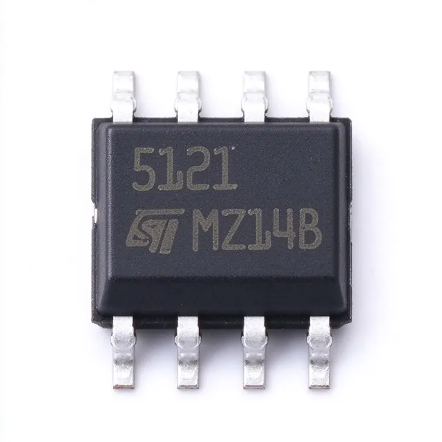
TS514ID
TS514ID - High-Speed Precision Quad Op Amp | STMicroelectronics
STMicroelectronics TS514ID is a high-speed, precision quad operational amplifier with four amplifier circuits, internally compensated frequency and phase response, short-circuit protection, internal ESD protection, and a 14-pin SOIC package. The verified product data identifies a maximum offset voltage of 500 uV and highlights a high gain-bandwidth product, low distortion, low noise, low power consumption, and high channel separation. The TS514ID is intended for instrumentation and general-purpose precision signal-processing designs requiring four amplifiers in one package.
An operational amplifier, commonly called an op amp, is a voltage-controlled differential amplifier with very high open-loop gain. Its external feedback network determines the closed-loop behavior. The TS514 belongs to the operational-amplifier hierarchy, which includes instrumentation amplifiers, buffer amplifiers, comparators, and general-purpose voltage amplifiers. Internal phase compensation allows the TS514 to operate as a voltage follower despite its high gain-bandwidth product, reducing the external compensation effort required in many designs.
The quad architecture integrates four amplifier channels into one 14-pin SOIC-14 package. Verified manufacturer-related product descriptions identify low offset voltage, low power consumption, short-circuit protection, low distortion, low noise, high gain-bandwidth product, high channel separation, and internal ESD protection. These characteristics make the device applicable to precision buffering, signal conditioning, instrumentation, industrial measurement, and general analog signal-processing systems. Each amplifier requires stable supply decoupling and careful handling of output-current limits.
The TS514 uses internal frequency and phase compensation. This architecture is particularly useful in follower and precision-gain configurations because the compensation is already incorporated into the device. Its high speed does not eliminate the need for short feedback traces, adequate grounding, and supply bypassing. Designers should avoid long output routing and place input, output, and ground returns so that parasitic capacitance does not degrade stability or transient response.
Typical uses include four-channel sensor conditioning, low-level signal amplification, active filtering, voltage buffering, and instrumentation chains requiring several matched amplifier functions. Industrial control and test equipment can also use the quad package to reduce board area compared with four discrete single-amplifier packages. Where precision offset and noise dominate, the complete manufacturer datasheet should be consulted for test conditions and application-specific limits.
The principal design trade-off is speed versus power and stability margin. Although the TS514 supports high-speed operation and voltage-follower use, board layout, capacitive loading, output-current demand, and supply bypassing remain critical. A short, low-inductance layout with local decoupling is recommended. Application notes and the manufacturer datasheet should control the final compensation, grounding, and thermal implementation.
This product page combines verified distributor and datasheet information with practical guidance on precision analog design, package reuse, selection criteria, and drop-in alternatives. It also distinguishes confirmed TS514-family candidates from cross-package or merely functional substitutes so engineers can avoid redesigns that require PCB changes.
询价
联系我们