产品(38,000+)

W9751G6KB-25-TR - 512Mb DDR2 SDRAM x16 84-WBGA | Winbond
W9751G6KB-25-TR

W9751G6KB-25-TR - 512Mb DDR2 SDRAM x16 84-WBGA | Winbond

The Winbond W9751G6KB-25-TR is a 512 Mbit (32M x 16) Double Data Rate 2 (DDR2) Synchronous DRAM organized as 8M words x 4 banks x 16 bits, housed in an 84-ball WBGA (8 x 12.5 mm) package supplied on tape and reel. It supports a 400 MHz DDR2-800 data rate, equivalent to 57.5 ns clock cycle time, and operates from a 1.7 V to 1.9 V supply with a commercial 0 C to 85 C temperature range. The device uses SSTL_18-compatible stub-series terminated logic I/O to deliver 800 MT/s peak transfer per pin. A DDR2 SDRAM is a synchronous dynamic random-access memory that transfers two data words per clock cycle on both rising and falling edges, doubling peak throughput compared with DDR1 at the same clock rate. DDR2 sits in the SDRAM hierarchy between DDR1 and DDR3, with lower power (1.8 V VDD), higher prefetch (4n), and on-die termination that improves signal integrity on densely routed DIMM or SoC fly-by topologies. It is the standard commodity DRAM of the late-2000s era and remains widely second-sourced today for industrial, set-top, networking, and embedded designs. Key features of the W9751G6KB-25-TR include a 16-bit-wide data interface, 4-bank architecture supporting concurrent operations, programmable CAS Latency (CL), Additive Latency (AL), and Write Latency (WL) to ease controller timing closure, and on-die termination (ODT) for signal-integrity tuning. The 84-WBGA package with 8 x 12.5 mm outline offers a compact footprint for space-constrained boards, while the industrial-commercial temperature window covers most non-automotive embedded environments. The device integrates Winbond's standard DDR2 mode-register set, refresh logic, and self-refresh / power-down modes for low standby current. Programmable burst lengths of 4 and 8 plus burst-chop and burst-interrupt sequences allow efficient DDR2 controller interfacing. The 25 in the part number (W9751G6KB-25) corresponds to the -25 speed grade (CL5 equivalent), supporting 400 MHz operation. Typical applications include IPTV/set-top box main memory buffering, low-end networking line cards, industrial HMI panels, surveillance DVR frame buffers, and consumer-electronics motherboards that still support DDR2 memory. The 512 Mbit density slots in where 64 MB of working memory is needed without the cost of 1 Gb densities. When designing with this part, observe the JEDEC DDR2 fly-by topology recommendations: route command/address/control/clock in a daisy-chain from the controller to the DRAM, place VREF and VTT termination as recommended, and provide a 100 nF plus bulk decoupling near each VDD/VSS pair. This page synthesizes current distributor pricing, drop-in equivalents from Winbond and competitor sources, and practical PCB-layout notes not aggregated on any single manufacturer or distributor page.

询价 联系我们
W9751G6NB-25 - 512Mb DDR2-800 SDRAM x16 | Winbond
W9751G6NB-25

W9751G6NB-25 - 512Mb DDR2-800 SDRAM x16 | Winbond

The Winbond Electronics W9751G6NB-25 is a 512 Mbit DDR2 SDRAM memory IC organized as 8,388,608 words x 4 banks x 16 bits (32M x 16), operating at a 400 MHz clock with DDR2-800 data rates and a 57.5 ns access time, housed in an 84-ball VFBGA (8 x 12.5 mm) package. DDR2 SDRAM (Double Data Rate 2 Synchronous Dynamic Random Access Memory) is a type of volatile semiconductor memory that transfers data on both the rising and falling edges of the clock signal, doubling effective bandwidth compared to single data rate SDRAM. Within the memory hierarchy, DDR2 SDRAM sits below DDR3 and DDR4 in performance but remains widely used in cost-sensitive embedded systems. The broader taxonomy runs: DDR2 SDRAM -> SDRAM -> DRAM -> semiconductor memory -> memory IC. Key features of the W9751G6NB-25 include an auto precharge function for simplified memory controller operation, a data mask (DM) function for selective byte writes, and dynamic on-chip termination (ODT) that improves signal integrity at high data rates by terminating the bus at the die rather than on the motherboard. These on-die features reduce external component count and strengthen signal integrity in dense PCB layouts. Technically, the device achieves transfer rates up to DDR2-800 with the -25 speed grade suffix, operating from a 1.8 V supply per the DDR2 JEDEC standard. Winbond sorts the W9751G6NB family into speed grades -18, -25, and -3 (with I and J industrial variants), allowing designers to scale performance within an identical footprint. The 84-ball VFBGA ball map follows the standard DDR2 x16 JEDEC footprint, ensuring controller and PCB compatibility across the family. Typical applications include embedded computing boards, industrial PCs, networking equipment, set-top boxes, and legacy desktop/laptop memory module repair where DDR2 is still required. The x16 organization suits low-cost controllers with narrower 16-bit buses, and its proven presence in systems such as the Dell Latitude D630 demonstrates field reliability. A key design consideration: DDR2 termination must follow the dynamic ODT settings in the Winbond datasheet, and VREF rails require clean, low-noise routing for timing margins to hold across the full 0 to 85 C commercial temperature range. This page synthesizes distributor pricing, drop-in alternatives, and practical design notes not found in the manufacturer datasheet.

询价 联系我们
W9812G6KH-6 - 128Mb SDRAM x16 166MHz 54-TSOP II | Winbond
W9812G6KH-6

W9812G6KH-6 - 128Mb SDRAM x16 166MHz 54-TSOP II | Winbond

The Winbond W9812G6KH-6 is a 128 Mbit synchronous DRAM (SDRAM) organized as 2M words x 4 banks x 16 bits, housed in a 54-pin TSOP II package with a 166 MHz clock rate and LVTTL interface. It delivers up to 200 M words per second of data bandwidth through a single 16-bit I/O bus running at a 5 ns cycle time, making it a mainstream density for embedded SDRAM sockets. A Synchronous DRAM (SDRAM) is a dynamic random-access memory that synchronizes its operation with an external clock, enabling pipelined, multi-bank burst access. Within the broader memory hierarchy, SDRAM sits between asynchronous DRAM and modern DDR/DDR2/3/4 SDRAM. This 128 Mb density represents the high end of single-chip SDRAM and is widely used in legacy MCUs, SoCs, FPGA soft-processors and consumer ASICs that integrate an SDRAM controller but no DDR PHY. The "-6" speed grade corresponds to a 166 MHz / 200 Mbps/pin class device. Key features include four internal banks for concurrent operation, programmable CAS Latency of 2 or 3, a 64 ms refresh interval (8 K cycles), and 3.3 V single-supply operation with LVTTL-compatible I/O. The 54-pin TSOP II footprint is the industry-standard JEDEC pinout for 16-bit SDRAMs, ensuring socket compatibility with second-source parts. The device supports sequential, interleaved and burst-terminate burst modes, and offers low-power features including Power-Down and Self-Refresh modes. The W9812G6KH-6 is fabricated on a CMOS process and is built around four banks of 2M x 16 cells, each with a sense-amplifier and row/column decoder pipeline. The 5 ns clock-to-access time at 166 MHz matches PC133 SDRAM timing, and the device is fully synchronous to the positive edge of the system clock. The interface uses a single 16-bit DQ bus shared by all banks, with separate DQM byte-mask controls to enable byte-write operations. Typical applications include set-top boxes, network printers, IP cameras, point-of-sale terminals, and industrial HMI panels. It also serves as main memory for mid-range MCUs such as the Winbond W90N745, NXP i.MX family, and various FPGAs with embedded SDR controllers. The wide ecosystem of compatible second-source parts makes it a low-risk design choice. When designing with the W9812G6KH-6, observe the JEDEC SDRAM 16-bit TSOP II routing topology - keep DQ/DQS/CLK traces matched within the prescribed skew window and provide a low-impedance VDD/SS plane beneath the package. Decoupling should use 0.1 uF ceramics at every VDD/VSS pair. Termination is generally not required for clock rates up to 166 MHz when traces are kept short. This page synthesizes distributor pricing from DigiKey, Mouser, LCSC and Octopart, drop-in alternatives from the Winbond W9812G6KH speed-grade family, and cross-vendor pin-compatible replacements from the JEDEC 128 Mb x16 SDRAM category - data not aggregated in any single manufacturer datasheet.

询价 联系我们
W9812G6KH-6-TR - 128Mb SDR SDRAM 166MHz LVTTL 54-TSOP II | Winbond
W9812G6KH-6-TR

W9812G6KH-6-TR - 128Mb SDR SDRAM 166MHz LVTTL 54-TSOP II | Winbond

The Winbond W9812G6KH-6-TR is a 128 Mbit synchronous dynamic random access memory (SDRAM) device organized as 2M words × 4 banks × 16 bits (8M × 16), supplied in a 54-pin TSOP II package and operating from a 3.3 V LVTTL interface at a clock frequency of 166 MHz with a 5 ns access time. It conforms to the JEDEC standard for 128 Mb SDRAM and supports sequential and interleaved burst modes of 1, 2, 4, 8, or full page. A SDR SDRAM (synchronous DRAM) is a volatile memory technology that synchronizes all read/write operations to a system clock, in contrast to older asynchronous DRAM. It belongs to the SDRAM family within the broader DRAM hierarchy, itself a category of volatile random-access memory used as main working memory and frame buffers. SDR SDRAM preceded DDR, DDR2, DDR3 and subsequent double-data-rate generations and remains in legacy industrial, automotive infotainment, set-top box, printer, and embedded designs where interface compatibility and low cost outweigh bandwidth demands. Key features include self-refresh mode for low-power standby, power-down mode, programmable CAS latency of 2 or 3, auto precharge and auto refresh, and a deep power-down option. The device supports LVTTL inputs and is fully synchronous with positive-edge clocked control. Operating current is approximately 130 mA (active) and self-refresh current is typically under 1 mA, making it suitable for battery-backed or energy-conscious designs. Architecturally, the W9812G6KH-6-TR combines four internal banks that can operate independently, allowing concurrent row activation across banks for improved throughput at high command rates. Each bank contains 2M words of 16-bit cells; the chip therefore presents an 8M × 16 logical organization. Programmable mode register settings control burst length, burst type, CAS latency and write mode. Typical applications include industrial control mainboards, legacy PC graphics frame buffers, network routers, set-top boxes, printers, scanners, digital still cameras, and embedded Linux boards using SDRAM-equipped SoCs. The wide operating temperature and stable supply tolerance make it especially attractive for long-life industrial designs. Designers should pay attention to PCB trace length matching of the clock, DQ, DQS and command/address groups. Improper impedance control on a 54-TSOP II footprint can introduce access-time violations at 166 MHz; reference Winbond application guidance for 50 Ω single-ended traces. This page synthesizes current distributor pricing for the W9812G6KH-6-TR, lists pin-compatible same-brand and cross-brand drop-in alternatives (W9812G6JH-6, W9812G6KH-6I, IS42S16160B, MT48LC8M16A2) and provides design notes that complement the official Winbond datasheet.

询价 联系我们
W9812G6KH-6I TR - 128Mb SDRAM 166MHz 3.3V | Winbond
W9812G6KH-6I TR

W9812G6KH-6I TR - 128Mb SDRAM 166MHz 3.3V | Winbond

The Winbond Electronics W9812G6KH-6I TR is a 128Mbit synchronous dynamic random access memory (SDRAM) organized as 2M words x 4 banks x 16 bits, operating at up to 166 MHz with a 3.3V LVTTL interface in a 54-pin TSOP-II package, supplied on tape and reel for automated assembly. An SDRAM is a type of DRAM that synchronizes all address, data, and control signals to a system clock, allowing pipelined burst accesses at the clock edge. Within the memory hierarchy, SDRAM sits above asynchronous DRAM (FPM/EDO) and below DDR generations, and remains the standard volatile memory choice for microcontroller, DSP, and FPGA systems that lack DDR controllers. The W9812G6KH family belongs to the broader DRAM and volatile memory IC category. Key features include a 166 MHz clock rate at CL3 (-6I speed grade), a data bandwidth of up to 200M words per second, four internal banks with interleaved operation to hide precharge and row-to-row delays, and programmable CAS latency and burst lengths (1, 2, 4, 8, or full page). The industrial temperature rating (-40C to +85C) makes the -6I grade suitable for harsh environments. Technically, the device uses a synchronous interface with row and bank activation commands, auto-refresh and self-refresh modes, and auto/precharge options per the standard SDRAM command set. Power is supplied at a nominal 3.3V with LVTTL logic levels, and clock-enable (CKE) support allows power-down for reduced standby current. Typical applications include embedded controller buffering, network equipment line-card memory, industrial HMI frame buffers, and FPGA-based data acquisition systems where an SDR SDRAM controller is already implemented. A key design consideration is refresh budgeting: allocate tRFC and 4096 refresh cycles per 64 ms into your controller scheduling, and terminate clock and address lines appropriately at 166 MHz to maintain signal integrity on a 54-pin TSOP-II footprint. This page synthesizes distributor pricing, drop-in alternatives across Winbond and ISSI, and practical design notes not found in the manufacturer datasheet.

询价 联系我们
W9816G6JH-6 - 16Mb SDR SDRAM, 166 MHz, TSOP-50 | Winbond
W9816G6JH-6

W9816G6JH-6 - 16Mb SDR SDRAM, 166 MHz, TSOP-50 | Winbond

The Winbond W9816G6JH-6 is a 16 Mbit synchronous DRAM (SDRAM) organized as 512K words x 2 banks x 16 bits, operating at a clock frequency of 166 MHz with a 5 ns column access time in a 50-pin TSOP II package. The W9816G6JH-6 is the speed grade -6 variant in a family that includes -5, -6, -6I (industrial temperature), -7, and -7I variants, delivering up to 200M words per second of data bandwidth per the Winbond datasheet. An SDR SDRAM is a synchronous dynamic random-access memory that uses a single-ended clock to synchronize command, address, and data transfers on a rising edge. SDRAM sits in the memory hierarchy between asynchronous SRAM (lowest density, no refresh, simpler) and later-generation DDR SDRAM (higher bandwidth via double data rate and on-die termination). It belongs to the broader category of volatile memory ICs, where each bit is stored on a capacitor-refreshed cell. The W9816G6JH-6 features a 16-bit data bus, two internal banks for interleaved operation, and a synchronous interface driven by CLK, CKE, /RAS, /CAS, /WE, /CS, and DQML/DQMH byte-mask lines. Self-refresh and power-down modes are supported for low standby power, and the device operates from a 3.3 V supply typical for SDR SDRAM. The 50-TSOP II package (10.16 mm body width) is the JEDEC standard form factor for SDR SDRAM, enabling direct drop-in replacement in legacy embedded designs. Typical applications include embedded Linux/MCU systems requiring bulk volatile memory (set-top boxes, industrial controllers, printers, automotive infotainment of its era), legacy networking equipment with 16-bit external memory buses, and graphic LCD frame buffers. The 5 ns access time makes it suitable for ARM7/ARM9-class processors and older MIPS cores that interface to SDRAM at 100-166 MHz. The two-bank architecture supports interleaved row activation that reduces precharge latency in streaming workloads. When designing with this part, observe JEDEC standard PCB layout rules for TSOP-50: keep data, address, and clock traces matched within ±25 ps, maintain a continuous ground plane beneath the package, and use VSS/VCCQ decoupling capacitors within 5 mm of the supply pins. Because this is a 3.3 V parallel SDRAM, confirm that the host controller's external memory interface supports the LVTTL levels used by the W9816G6JH-6 before layout commit. The W9816G6JH-6I variant adds industrial temperature range (-40C to +85C) for harsh environments. This page synthesizes cross-reference candidates, parametric comparisons, and design notes from the Winbond datasheet and distributor listings that are not aggregated on a single product page elsewhere.

询价 联系我们
W9825G6KH-6 - 256Mb 166MHz SDR SDRAM | Winbond | 54-TSOP II
W9825G6KH-6

W9825G6KH-6 - 256Mb 166MHz SDR SDRAM | Winbond | 54-TSOP II

The Winbond Electronics W9825G6KH-6 is a 256Mbit (16M x 16) Synchronous DRAM (SDRAM) memory IC operating at 3.3V with a clock speed of 166 MHz in a 54-pin TSOP II surface-mount package. The -6 speed grade delivers a data bandwidth of up to 200M words per second, making it one of the most widely used external RAM devices in cost-sensitive embedded systems. SDRAM (Synchronous Dynamic Random Access Memory) is a class of DRAM synchronized to the system clock, allowing a memory controller to execute commands - activate, read, write, precharge - on defined clock edges rather than asynchronously. Within the memory hierarchy, SDRAM sits between on-chip SRAM caches and non-volatile storage such as NOR/NAND flash, providing megabytes of fast working memory for processors that lack sufficient internal RAM. Key features of the W9825G6KH include a x16 organization (16,777,216 words x 16 bits), four internal banks with burst lengths of 1, 2, 4, 8, or full-page, and programmable CAS latency. The device complies with the personal computer industrial standard for SDRAM and is sorted into speed grades -5, -5I, -6, -6I, -6J, -6L, -75, 75J and 75L per the Winbond datasheet, so the -6 grade designates the commercial-temperature 166 MHz version. Technically, the W9825G6KH uses a four-bank architecture with row and column addressing (12 row address lines, 8 column address lines for x16), bank activate/read/write/precharge commands, and auto-refresh with self-refresh entry for low-power standby. Two DQM (data mask) pins enable byte-lane masking on the 16-bit bus, and mode register programming selects burst length, burst type, and CAS latency. Typical applications include external memory expansion for STM32, NXP i.MX RT, and other MCUs/MPUs with SDRAM controllers, industrial HMI display frame buffers, network appliance buffers, and data acquisition buffering. Its 3.3V interface and standard TSOP II footprint keep board-level integration simple. Design consideration: maintain proper signal integrity by keeping clock, DQM, and address traces length-matched, and implement the full auto-refresh schedule required by the controller to prevent data loss. This page synthesizes distributor pricing, verified drop-in alternatives, and practical design notes not found in the manufacturer datasheet.

询价 联系我们
W9864G6JH-6 - 64Mb SDRAM 4Mx16 166MHz TSOP-54 | Winbond
W9864G6JH6

W9864G6JH-6 - 64Mb SDRAM 4Mx16 166MHz TSOP-54 | Winbond

The Winbond W9864G6JH-6 is a 64-Mbit high-speed synchronous dynamic random access memory (SDRAM) organized as 1M word x 4 banks x 16 bits, housed in a 54-pin TSOP-II (Type II) package. It supports a 166 MHz clock rate with a 5 ns access time and operates from a single 3.3 V supply (3.0 V to 3.6 V). The device uses a 4-bank architecture with bank-active/auto-refresh/self-refresh modes, delivering up to 200M words per second of data bandwidth on a 16-bit data bus. An SDRAM (Synchronous Dynamic Random Access Memory) is a class of volatile DRAM that synchronizes all timing with the system clock, replacing older asynchronous DRAM and enabling pipelined burst operations. It sits in the memory hierarchy between cache and mass storage, offering higher density than SRAM at lower cost, and is a member of the broader semiconductor memory family that includes SRAM, NOR flash, and NAND flash. SDRAM parts are organized as banks, rows, and columns; commands (RAS, CAS, READ, WRITE, PRECHARGE, REFRESH) are latched on the rising clock edge. Key features of the W9864G6JH-6 include programmable CAS latency of 2 or 3, programmable burst length of 1, 2, 4, 8, or full page, auto-refresh and self-refresh power-down modes, LVTTL-compatible I/O, and LVCMOS-compatible address/command inputs. The TSOP-II 54-pin, 0.4-inch-wide, 0.65 mm-pitch package is the industry-standard JEDEC footprint for x16 SDRAM, allowing PCB reuse across densities and vendors. Power dissipation is low because the device enters self-refresh during idle periods and supports a power-down mode that disables the clock when no operation is in progress. Architecturally, the W9864G6JH-6 uses four internal banks that allow concurrent row activation while another bank is being read or written, effectively doubling the throughput compared with single-bank DRAM of similar speed grade. The -6 speed suffix indicates a 166 MHz CAS-3 grade, which the Winbond datasheet specifies as 5 ns tRAC / 5 ns tAC / 2 ns tOH. The LVCMOS/LVTTL interface is fully compliant with 3.3 V logic levels used by PCI, MPEG, and embedded MCU/ASIC hosts. Typical applications include set-top box video buffers, set-top box MPEG transport stream buffers, networking line cards, industrial controllers, printers, and any embedded system that needs a low-density, low-cost synchronous DRAM. In modern designs the part is most often chosen for legacy or cost-sensitive platforms that have not yet migrated to DDR/DDR2/LPDDR. When designing with the W9864G6JH-6, place a 0.1 uF decoupling capacitor close to each VDD pin and provide a 22 ohm series resistor on the clock line to damp overshoot; respect the JEDEC refresh interval of 15.6 us at 0-70 C to retain data.

询价 联系我们
W989D6DBGX6I - 512Mbit Mobile LPSDR SDRAM x16 166MHz | Winbond
W989D6DBGX6I

W989D6DBGX6I - 512Mbit Mobile LPSDR SDRAM x16 166MHz | Winbond

The Winbond Electronics W989D6DBGX6I is a 512Mbit (32Mx16) Mobile Low-Power SDRAM (LPSDR) memory IC organized as 32M words x 16 bits, operating from a single 1.8V supply at a 166 MHz clock rate with 5 ns access time, and housed in a 54-ball VFBGA (8x9) package. The device is fabricated on a 46 nm CMOS process and supports the industry-standard JEDEC LPSDR interface with self-refresh and partial-array self-refresh (PASR) modes that minimize standby power in battery-powered designs. Mobile LPSDR SDRAM is a derivative of the standard SDRAM specification optimized for handheld and portable applications. It is a synchronous dynamic random-access memory, meaning it stores each bit in a separate capacitor inside an array of memory cells, and is refreshed periodically to retain data. Compared with standard SDRAM, LPSDR adds partial-array refresh, temperature-compensated self-refresh, and a deep power-down mode, which dramatically reduce the average current draw in standby. Architecturally LPSDR belongs to the SDRAM family, which in turn is part of the volatile memory hierarchy below SRAM and above NOR/NAND flash in cost per bit. Key features of the W989D6DBGX6I include a x16 data interface, four internal banks for concurrent operation, programmable CAS latency of 2 or 3, programmable burst length of 1, 2, 4, 8, or full page, and on-chip temperature compensation for self-refresh current. The VFBGA-54 (8x9) package measures only 8 mm x 9 mm with a 0.8 mm ball pitch, making it suitable for space-constrained PCB layouts where thin-profile memory stacking is required. The device operates across the industrial -40C to +85C temperature range, designated by the trailing "I" suffix in the MPN. Typical applications for the W989D6DBGX6I include smartphone baseband buffers, wearable and smartwatch frame buffers, portable media player RAM, automotive infotainment working memory, industrial HMI panels, and IoT edge devices that need 32 MB of low-power working RAM. The 1.8V VDDQ/JEDEC-compliant LPSDR interface allows direct connection to common application processors and SoCs that expose an LPSDR/LPDDR controller. When designing with the W989D6DBGX6I, observe the JEDEC LPSDR PCB layout guidelines: keep the 16 data lines (DQ0-DQ15), clock (CLK), clock-enable (CKE), and the command/address bus length-matched within ±25 mil, place a 0.1 µF decoupling capacitor per VDD pin within 100 mil of the ball, and reserve a continuous ground plane beneath the package. The partial-array self-refresh register must be configured during initialization to achieve the lowest standby current in always-on applications. This page synthesizes distributor pricing, drop-in alternatives within the same VFBGA-54 footprint, and practical PCB design notes that go beyond the bare datasheet content.

询价 联系我们
W989D6DBGX6I-TR - 512Mb Mobile LPSDR SDRAM, x16, 166MHz | Winbond
W989D6DBGX6I-TR

W989D6DBGX6I-TR - 512Mb Mobile LPSDR SDRAM, x16, 166MHz | Winbond

The Winbond W989D6DBGX6I-TR is a 512Mb (32M x 16) Mobile Low-Power SDR (LPSDR) SDRAM organized as 16-bit wide data, operating at 5 ns clock period (166 MHz), in a 54-ball VFBGA (8x9) package, and supplied from a 1.8 V rail. It is built on a 46 nm process node and qualified to industrial temperature range (-40C to +85C). The suffix -TR denotes tape-and-reel packing for high-volume SMT assembly. A Mobile LPSDR SDRAM is a class of low-power dynamic random-access memory that follows the JEDEC LPSDR standard (a low-voltage derivative of the SDR SDRAM family) designed for portable consumer electronics. It fits into the hierarchy LPSDR -> SDR SDRAM -> DRAM -> volatile memory -> semiconductor. LPSDR devices traditionally serve mobile phones, PMPs, GPS modules and other handhelds where 1.8 V I/O, low standby current and deep power-down modes are required. Compared with classic 3.3 V SDR SDRAM, Mobile LPSDR cuts I/O power roughly in half. Key features of the W989D6DBGX6I-TR include: 512 Mbit density, x16 organization (32M words x 16 bits), 166 MHz / 5 ns maximum clock rate, 1.8 V single supply, four internal banks, and selectable CAS Latency (CL=2/3). The 46 nm process enables lower active current than the previous 60-90 nm generations of Winbond Mobile SDR. The device supports standard SDRAM commands: MRS, REF, ACT, PRE, RD, WR, plus partial-array self-refresh (PASR) and a deep power-down (DPD) mode for battery saving. Architecturally, the W989D6DBGX6I-TR uses a 4-bank page-mode architecture with a 1024-cycle refresh window. Each bank contains 8K rows of 1K x 16 bits. The 16-bit wide host bus simplifies connection to mobile application processors with 16-bit SDR controllers, eliminating external bus-width conversion. The 54-ball VFBGA (8 mm x 9 mm) footprint allows reflow-compatible SMT assembly with controlled impedance routing for clock, DQS and data nets. Typical applications include mobile phone main displays and user-interface framebuffers, portable media players (PMP), handheld gaming devices, GPS/PDA terminals, digital photo frames, low-end tablet controllers, automotive infotainment secondary displays, and embedded Linux devices that need a low-cost 16-bit external RAM expansion. The industrial temperature range also makes the part suitable for in-cabin automotive, outdoor signage, and rugged industrial handhelds. When designing with this device, pay attention to PCB layout: route CK, CK# and DQS as length-matched, 50 ohm controlled-impedance pairs; place 0.1 uF plus 1 uF decoupling near each VDD/VDDQ ball; and follow the Winbond Mobile LPSDR layout checklist for VFBGA break-out. Power-rail sequencing must observe tRCD=18 ns, tRP=18 ns, and tRFC=110 ns; failure to meet these will corrupt refresh and lose data. This page synthesizes distributor pricing (Mouser, DigiKey, LCSC, Octopart), 5-8 drop-in alternatives, application notes, and design guidance not found on the manufacturer datasheet, giving buyers and engineers a single source for selection.

询价 联系我们
W9968CF - USB 1.1 Digital Camera Controller IC | Winbond
W9968CF

W9968CF - USB 1.1 Digital Camera Controller IC | Winbond

The Winbond W9968CF is a digital camera controller IC with a built-in full-speed USB 1.1 controller, integrating JPEG still-image compression and a dedicated video/image processing pipeline in a 128-pin PQFP (14 x 20 mm, 2.75 mm height) package. It is designed as a single-chip bridge between CMOS/CCD image sensors and a PC USB port for webcam and digital still camera products. A digital camera controller (also called a camera bridge or image coprocessor) is a specialized embedded processor that acquires raw pixel data from an image sensor, processes and compresses it, and streams it to a host interface. In the system hierarchy it sits between the image sensor and the USB physical layer, complemented by external SDRAM/DRAM frame memory and an MCU or sensor controller. Key features of the W9968CF, per Winbond documentation, include native support of USB Specification Revision 1.1, use of the isochronous transfer mode for continuous video streaming, and full compliance with USB power-management requirements covering startup, operating, and suspend modes. On-chip JPEG compression hardware reduces USB bandwidth consumption, allowing higher effective frame rates or resolutions than uncompressed streaming. The revision history of the Winbond datasheet documents formal releases in April 1998 (Revision A1) and May 1999 (Revision A2); Revision A2 changed the bcdUSB and bcdDevice descriptor values to 0x0110 to reflect USB 1.1 compliance and added the CR39_4 register bit for JPEG clock enable, indicating a register-configurable image pipeline. The device is classified by distributors as a Consumer Circuit / Specialized IC in the QFP-128 package family (surface mount). Typical applications are PC webcams, low-cost digital still cameras, video capture dongles, and embedded USB camera modules where a single-chip sensor-to-USB bridge reduces BOM cost. Design consideration: verify the image sensor interface timing and external memory configuration against the manufacturer datasheet, as the W9968CF requires matching sensor clocking and frame-buffer memory to meet isochronous bandwidth limits. This page synthesizes distributor availability, datasheet revision data, and sourcing context not consolidated in the original Winbond datasheet.

询价 联系我们
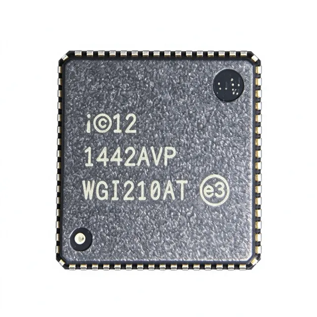
WGI210AT - Intel I210-AT Gigabit Ethernet Controller QFN-64 | Intel
WGI210AT

WGI210AT - Intel I210-AT Gigabit Ethernet Controller QFN-64 | Intel

The Intel WGI210AT (also marketed as the Intel Ethernet Controller I210-AT) is a single-chip, PCIe-based Gigabit Ethernet controller that supports 10BASE-T, 100BASE-TX, and 1000BASE-T operation, packaged in a 9 mm x 9 mm 64-pin QFN with an exposed thermal pad. It integrates a PCIe v2.1 (2.5 GT/s) host interface, a GMII/RGMII/MII MAC, and on-chip PHY, delivering full IEEE 802.3 compliance for enterprise, industrial, and embedded networking designs. The device uses a 0.9 V internal core supply with a 3.3 V I/O supply, enabling low power consumption typical of 1 W class GbE controllers. A Gigabit Ethernet controller is a purpose-built networking IC that links a host processor (typically via PCIe) to a copper or fiber physical network, handling MAC/PHY framing, link training, and TCP/UDP/IP checksum offload. Within Intel's Ethernet controller taxonomy, the I210 sits in the lower-power mainstream tier below the I350/I210 server parts, optimized for single-port embedded and small-form-factor designs. PCIe is the standard host interconnect for these controllers, replacing the older PCI-X interfaces that preceded the GbE era. Key features include TimeSync offload (IEEE 1588/802.1AS) for industrial automation, energy-efficient Ethernet (EEE) per IEEE 802.3az, jumbo frame support up to 9.5 KB, and the proven Intel PROSet driver stack. The exposed pad of the QFN-64 package provides a low-thermal-resistance path to the host PCB, a critical feature since GbE PHYs can dissipate 600 mW to 1.2 W during continuous full-duplex operation. On-die MACsec and VLAN stripping/insertion further reduce host CPU overhead. Architecturally, the I210 uses a PCI Express 2.1 endpoint controller with one x1 lane, hardware IEEE 802.1Qav time-sensitive-networking shaping, and an integrated 1000BASE-T PHY capable of auto-negotiation across all three link rates. The MAC supports 9.6 KB jumbo frames, IPv4/IPv6 checksum offload, TCP segmentation offload (TSO v2), and iSCSI boot for SAN-attached storage platforms. This combination of MAC, PHY, and PCIe in a single 64-pin QFN distinguishes the I210 from external-PHY controllers. Typical applications include industrial PCs, factory automation controllers, point-of-sale terminals, network printers, embedded routers, and small business servers. For automotive and industrial-grade designs with extended temperature requirements, Intel offers the pin-compatible WGI210IT variant rated for -40 C to +85 C operation rather than the 0 C to +70 C commercial range of the WGI210AT. When designing with this controller, allocate at least four PCB layers with a continuous ground plane beneath the QFN-64 exposed pad to keep junction temperature below 110 C; provide 4 kV ESD protection on the MDI lines; and verify driver compatibility with your OS kernel (Windows, Linux, VxWorks, or RTOS). The PCIe reference clock must be a 100 MHz HCSL source with the impedance and jitter specified in the Intel I210 datasheet. This page synthesizes distributor pricing as of 2026-10-11, drop-in alternatives from the same I210 family, and practical layout notes that complement the Intel datasheet with cross-reference insight not found on a single OEM page.

询价 联系我们
WGI210AT-SLJXR - Intel I210-AT GbE Ethernet Controller QFN-64
WGI210AT-SLJXR

WGI210AT-SLJXR - Intel I210-AT GbE Ethernet Controller QFN-64

The Intel WGI210AT-SLJXR is an Intel Ethernet Controller I210-AT single-chip Gigabit Ethernet MAC + PHY in a 9x9 mm QFN-64 (9x9) package, supporting 10BASE-T, 100BASE-TX, and 1000BASE-T over PCIe, SGMII, SPI, JTAG, and I2C interfaces at 3.3 V supply and 0.9 V core. According to the I210-AT datasheet, the device integrates a GbE PHY with jumbo-frame support and Audio-Video Bridging / IEEE 802.1AS / 802.3az Energy Efficient Ethernet features for desktop, server, and embedded designs. An Ethernet controller is a mixed-signal integrated circuit that links a host system (typically a CPU or SoC) to a wired network, handling MAC address framing, PHY physical-layer termination, and offloading protocol tasks from the host CPU. It belongs to the broader network-interface category (NIC controller -> Ethernet controller -> mixed-signal IC -> semiconductor) and is essential wherever a deterministic, low-latency wired network connection is required. Ethernet controllers sit in the platform's input/output subsystem, bridging PCIe to copper media and providing the physical termination that magnetics and an RJ45 jack connect to. The I210-AT is Intel's mainstream GbE controller for non-server applications and supports the full media-negotiation trio of 10 Mbps, 100 Mbps, and 1000 Mbps. It exposes a PCIe v2.1 5 GT/s host interface for typical x1 edge-connector applications, alongside legacy SMBus, SPI, and JTAG for management and firmware update. Power is supplied through a 3.3 V main rail and a 0.9 V core rail, with full PHY-level Energy Efficient Ethernet (EEE) support reducing link power during idle periods. Industrial features include NC-SI / SMBus manageability, MAC address pre-programming, and platform firmware resiliency. Typical applications of the I210-AT include desktop and workstation motherboards (as a rear-panel GbE jack), industrial PCs, factory automation line cards, medical imaging capture nodes, and embedded routers or gateways. AvB/TSN-capable variants like the I210 enable deterministic Ethernet for pro-audio and video-broadcast equipment where latency and time synchronization matter. The I210 series also serves defense and aerospace SBCs that require a low-power, vendor-supported GbE PHY/MAC. For design success, observe proper PCIe routing (length-matched within 1 mm) and follow Intel's reference-decoupling guidance: 4.7 uF + 0.1 uF near each power pin with a solid ground return. Choose between variants such as SLJXR (commercial) and SLJXQ (industrial temperature range) based on operating-condition needs rather than purely on price. Designers using AVB/802.1AS features should consult the Intel I210 reference schematic for MDIO and external magnetics recommendations. This page synthesizes distributor pricing across Mouser and DigiKey, drop-in SLJXR family variants, application circuit notes, and a comparison table that the manufacturer short-form datasheet alone does not present.

USD $4.92 有现货
WGI210IS - Intel I210-IS Gigabit Ethernet Controller QFN-64
WGI210IS

WGI210IS - Intel I210-IS Gigabit Ethernet Controller QFN-64

The Intel WGI210IS is the industrial-temperature variant of the Intel® Ethernet Controller I210, a single-chip, low-power Gigabit Ethernet (10/100/1000 Mbps) controller with a PCI Express v2.1 (2.5 GT/s) host interface, packaged in a 64-pin QFN (9 mm × 9 mm) with exposed pad. Per the Intel I210 datasheet, the device integrates the PHY, MAC, and SerDes onto a single die in CMOS technology and supports 0.9 V / 3.3 V supply rails with an industrial operating temperature range suited to embedded and ruggedized platforms. Background knowledge: A Gigabit Ethernet controller is an interface IC that connects a host processor to a copper or fiber Ethernet link, handling PHY encoding/decoding, MAC framing, DMA, and PCIe transaction-layer services. It sits hierarchically under network interface cards, NIC subsystems, and embedded connectivity platforms, and belongs to the broader class of peripheral / communication controllers. Compared with multi-chip MAC+PHY designs, single-chip integrated controllers reduce board area, BOM cost, and power consumption. Key features include support for IEEE 802.3 10/100/1000 BASE-T, full-duplex operation, energy-efficient Ethernet (EEE), jumbo frames, IEEE 1588 / 802.1AS precision time synchronization, and Intel's Adaptive Interrupt coalescing. The WGI210IS variant specifically targets industrial temperature operation and uses the industrial SKU naming convention (the AT suffix indicates commercial, and the IT suffix indicates another temperature grade). Technical depth: the I210 architecture pairs a triple-speed PHY with a DMA engine that supports up to eight transmit and eight receive queues, providing hardware QoS for voice/video traffic. Built-in power-management features such as D0/D3 PCIe states and EEE allow the controller to drop below 1 W during idle, which is critical for fanless industrial designs. Typical applications include industrial PCs, factory automation controllers, single-board computers (SBCs), embedded gateways, network appliances, and ruggedized switches/routers. The PCIe v2.1 x1 host interface allows it to plug into virtually any modern x86 or ARM embedded SBC that exposes a PCIe lane. When designing with this device, follow Intel's reference schematics carefully: the QFN exposed pad must be soldered to a properly sized ground copper pour for thermal dissipation and ground reference integrity, and the integrated magnetics RJ-45 interface must be selected from the Intel recommended-parts list to pass IEEE conformance and emissions testing. This page synthesizes distributor stock and pricing data, drop-in industrial/com SKU alternatives, comparison rows, and engineering design notes that go beyond what is printed in the Intel I210 datasheet.

询价 联系我们
WM1824BGEDT - 24-Bit 192kHz Stereo DAC | Cirrus Logic
WM1824BGEDT

WM1824BGEDT - 24-Bit 192kHz Stereo DAC | Cirrus Logic

Cirrus Logic WM1824BGEDT is a 24-bit stereo audio digital-to-analog converter with a maximum sampling rate of 192kHz, an I2S digital interface, and a 16-pin TSSOP surface-mount package. The device provides two output channels and operates from a single supply, making it suitable for compact consumer audio, communications, and embedded multimedia systems. An audio DAC is a signal-conversion integrated circuit that accepts digital audio samples and produces corresponding analog voltage signals. In the product hierarchy, the WM1824BGEDT is a special-purpose ADC/DAC, more specifically a stereo audio DAC, which belongs to the broader family of data-conversion semiconductors. Its role is to convert an I2S data stream into left- and right-channel analog outputs for subsequent amplification, filtering, or line-level routing. The principal specifications are 24-bit resolution, a 192kHz sampling rate, two-channel stereo operation, and an I2S interface. The 24-bit format provides substantially more numerical resolution than conventional CD-audio formats, while the 192kHz capability supports high-rate digital audio streams. The single-supply architecture simplifies system power planning, and the surface-mount TSSOP package supports automated PCB assembly. The WM1824BGEDT uses its I2S interface to receive serial digital audio data and stereo channel information. A reconstruction or low-pass filtering stage removes out-of-band digital noise before the analog signals leave the converter. The manufacturer documentation also defines mute attenuation as the level difference between full-scale output and the muted output, providing an important metric for evaluating mute behavior. Typical uses include digital active speakers, compact stereo audio modules, consumer media equipment, and embedded systems that receive standard I2S audio from a digital audio processor. In each case, the converter is positioned after the digital audio source and before an analog output amplifier or line-output stage. System designers should preserve the required clock relationships, interface format, supply conditions, and analog-output topology from the manufacturer documentation. A key implementation consideration is the relationship between supply voltage, full-scale output range, and downstream analog headroom. The converter should be placed so that its digital interface and analog outputs meet the source and amplifier requirements without introducing avoidable ground offsets. PCB layout should keep the device close to its decoupling components and route sensitive analog outputs away from fast digital switching nodes. This page combines the verified WM1824BGEDT identification, package and interface characteristics with application guidance, comparison parameters, and sourcing information. It also distinguishes the verified tube-packaged ordering option from other manufacturing or reel-code variants rather than presenting them as electrically different replacements.

询价 联系我们
WM8044CFN Audio Channel IC | Texas Instruments
WM8044CFN

WM8044CFN Audio Channel IC | Texas Instruments

The Texas Instruments WM8044CFN is a programmable audio-channel integrated circuit offered in a package identified by the “CFN” ordering suffix. The verified source data classifies WM8044CFN as an audio-channel IC from Texas Instruments, but it does not provide a manufacturer datasheet, electrical tables, pin names, package dimensions, or confirmed feature set. Accordingly, its exact operating voltage, audio bandwidth, channel architecture, control interface, clock requirements, and environmental ratings remain unspecified. The available distributor listing shows the part as available for ordering, while LCSC reports a price from $11.4948 as of 2026-10-23. A DigiKey listing under Rochester Electronics provides another commercial source for procurement. What is a programmable audio-channel IC? It is an audio signal-processing semiconductor that receives, routes, filters, mixes, converts, or otherwise conditions audio signals under digital or analog control. Within the electronics hierarchy, an audio-channel IC belongs to audio signal-processing ICs, a specialized type of interface or logic-adjacent integrated circuit. Its exact architecture cannot be inferred safely from the generic distributor classification alone, so engineers should consult the original Wolfson or Texas Instruments documentation before schematic capture. The most decision-relevant verified features are the MPN, manufacturer association, and device category. Search results identify WM8044CFN as a Texas Instruments audio-channel device and also describe it as a WOLFSON programmable logic IC in one marketplace listing. That historical WOLFSON association may help locate archived documentation, but it is not sufficient proof that any similarly named part is electrically or pin-for-pin replaceable. Typical uses cannot be assigned safely without the datasheet. Audio-channel ICs may serve portable audio, digital home audio, communications, or interface systems, but those possibilities are not verified WM8044CFN applications. Likewise, no performance claim regarding signal-to-noise ratio, total harmonic distortion, sample rate, channel count, or power consumption is supported by the supplied evidence. For design-in work, the critical first step is to obtain the authoritative WM8044 family datasheet, register map, application circuit, and pin description. Do not infer connections from the CFN suffix or from distributor board-layout references. Check the exact pin count and exposed-pad requirements before PCB layout because neither value appears in the verified data. This page combines verified distributor availability, the $11.4948 LCSC starting price, category information, sourcing links, and explicit data gaps. It avoids fabricating electrical specifications or offering unverified drop-in substitutes, thereby supporting component identification and procurement while reserving engineering approval until the original manufacturer documentation is available.

询价 联系我们
WM8144-12CPT CPT Audio Channel IC | Texas Instruments
WM8144-12CPT

WM8144-12CPT CPT Audio Channel IC | Texas Instruments

Texas Instruments WM8144-12CPT is an audio-channel integrated circuit associated with the WM8144 family and supplied in the manufacturer’s CPT package designation. The verified distributor listing identifies the device as an audio-channel component, while the MPN’s “-12” option designation distinguishes it from related catalog entries. One distributor quoted a price of $4.5282 as of 2026-10-29, and another listing reported in-stock availability on the same date. Detailed electrical limits, signal-conversion resolution, clocking requirements, pin assignments, and environmental limits were not included in the supplied source records and therefore require confirmation from the manufacturer documentation before design release. An audio-channel IC is a semiconductor that processes, converts, buffers, or conditions audio signals within an audio signal chain. Such devices may form part of a signal path connecting microphones, line-level sources, analog-to-digital converters, digital-to-analog converters, amplifiers, and downstream digital audio processors. In the broader component hierarchy, the WM8144-12CPT belongs to the integrated-circuit category, the audio-special-purpose subcategory, and ultimately the broader semiconductor and signal-processing device families. The strongest verified procurement attributes are the exact manufacturer part number, Texas Instruments branding, audio-channel classification, CPT package suffix, distributor availability, and a quoted $4.5282 unit price as of 2026-10-29. The LCSC result explicitly reported the WM8144-12CPT as in stock, while DigiKey described the listing as available to buy and ship. These commercial signals are useful for preliminary sourcing but do not establish production status, quantity discounts, or long-term supply guarantees. The available search records do not expose verified specifications for supply voltage, analog input range, output type, sample-rate support, resolution, signal-to-noise ratio, clock interface, control interface, or channel architecture. Consequently, an engineer must not infer those values from the “-12” suffix or from generic descriptions of Wolfson audio devices. The correct procedure is to download the WM8144 family documentation, confirm the orderable suffix, and cross-check every electrical limit against the intended application. Typical design roles for this device family include audio acquisition, analog audio conditioning, and interfaces between analog audio sources and digital audio systems. Candidate deployments include industrial monitoring equipment, communications terminals, test and measurement instruments, and compact embedded audio products. The WM8144-12CPT should be selected only after verifying that its documented input range, conversion behavior, clocking, and interface requirements match the selected codecs, processors, and analog front end. The main procurement risk is that distributor snippets provide commercial information but omit the technical document needed for schematic capture. Before ordering, request the current manufacturer datasheet, confirm the exposed-pad or thermal requirements of the CPT package, and check pin compatibility for any replacement. Likewise, verify absolute maximum ratings, decoupling requirements, layout recommendations, and application-circuit values rather than copying a generic reference design. This page distinguishes verified catalog and purchasing facts from unavailable technical data, provides a direct manufacturer documentation link for review, and identifies candidate same-brand family alternatives without inventing unsupported electrical specifications. It is intended to accelerate sourcing and initial engineering review while preserving the need for datasheet-level validation before PCB release or production commitment.

询价 联系我们

WM8144CCPT Audio Channel IC | Texas Instruments
WM8144CCPT

WM8144CCPT Audio Channel IC | Texas Instruments

The Texas Instruments WM8144CCPT is an audio-channel integrated circuit listed by DigiKey Marketplace and Octopart, with the product categorized as an Audio Special Purpose device in the Audio ICs family. The verified distributor information identifies WM8144CCPT as an active part available for sourcing, but the supplied records do not provide a verified package, pin count, electrical ratings, or detailed functional specifications. The searchable part number and category indicate a dedicated audio signal-processing role rather than a general-purpose logic or power component. Engineers should obtain the manufacturer datasheet and confirm the exact land pattern before committing a replacement to an existing PCB. An audio-channel IC is a specialized integrated circuit that handles one or more functions within an audio signal chain, such as conditioning, conversion, channel selection, or control. These devices sit between audio sources and downstream amplifiers, converters, microphones, speakers, or digital audio processors. Their performance requirements commonly include low signal distortion, stable channel behavior, compatible logic levels, and electrical characteristics matched to the intended audio architecture. Because the verified WM8144CCPT records provide only the part identity and broad category, device-specific claims should not be inferred without the original Wolfson Microelectronics or Texas Instruments documentation. The visible sourcing records support three practical points about WM8144CCPT. DigiKey Marketplace labels it as an audio channel from Texas Instruments, Octopart lists it as an integrated circuit for audio special purposes, and Rochester Electronics distribution data reports active production status. The supplied pricing excerpt gives a starting unit price of $4.07 at one-unit quantity and mentions volume discounts at 10, 100, 500, and 1,000 units. Availability language differs among marketplaces, so a purchase decision should use a current authorized-distributor quote and manufacturer inventory confirmation. WM8144CCPT is most relevant to legacy or industrial audio platforms in which the original circuit was designed around this exact device. In such systems, preserving the original device is generally safer than selecting a generic audio IC with similar nominal functionality. Any substitute must be checked for exact package dimensions, lead pitch, exposed-pad requirements, pin assignments, supply voltage, clocking, control interface, analog performance, and lifecycle status. The verified information identifies Rochester Electronics as the source of the distributed WM8144CCPT offer, so procurement documentation should also confirm the original manufacturer and authorized sourcing chain. The key engineering constraint is that the available verified data is incomplete. Mounting type, operating-temperature range, package case, absolute maximum ratings, supply voltage, channel count, resolution, interface type, and pin assignments are not stated in the supplied records. These values must be read from the applicable manufacturer datasheet before schematic capture, footprint selection, or production release. This prevents the mistake of treating a distributor category label as a substitute for full electrical and mechanical documentation. A sound sourcing workflow is to compare the distributor listing, Rochester Electronics product record, and Octopart cross-reference data against the original system documentation. Confirm that the ordered suffix CCPT matches the required package and ordering configuration, then request current stock and traceable shipment details. For repair and redesign programs, also inspect the board assembly records for markings or bill-of-material entries that may reveal the original manufacturer designation. This page consolidates the verified sourcing status, pricing basis, category placement, and data gaps for WM8144CCPT while avoiding unsupported electrical claims. It is intended to support initial part identification and procurement research, not to replace the manufacturer datasheet, reference schematic, or board-level compatibility checklist.

询价 联系我们
WM8144CPT - 10-Bit CCD Imaging Data Converter | Texas Instruments
WM8144CPT

WM8144CPT - 10-Bit CCD Imaging Data Converter | Texas Instruments

The Texas Instruments WM8144CPT is an integrated 10-bit data-acquisition system for imaging applications, packaged in a 27-pin CPT surface-mount package. It combines the analog signal-conditioning functions required by CCD sensors with a 10-bit ADC and optional pixel-by-pixel image compensation. The supplied source identifies WM8144CPT as an audio-channel IC, while the family description identifies WM8144 as an integrated CCD-imaging data-acquisition system. Those descriptions should be reconciled against the original manufacturer documentation before using the part in a new design. A CCD image sensor is a semiconductor that converts accumulated light into analog charge and transfers that charge through output circuitry in a sequence. Because the resulting signal is weak, noisy, and often offset or gain mismatched, imaging systems require conditioning before digital conversion. An integrated data-acquisition IC reduces discrete circuitry and helps standardize the interface between the sensor output amplifier, analog-to-digital converter, and image-processing electronics. The WM8144 family provides the core functions needed for imaging: CCD-compatible analog signal conditioning, a 10-bit ADC, and optional pixel-by-pixel compensation. Compensation circuitry is used to correct sensor-column offsets, gain variations, dark current, or fixed-pattern effects before pixels are interpreted. The practical benefit is a more compact analog section, but final image quality still depends on sensor characteristics, clocking, grounding, reference quality, and system calibration. The exact suffix CPT denotes the supplied package/orderable variant, but the verified source set does not expose the full pin list, electrical ratings, ADC conversion rate, voltage limits, clock requirements, or operating-temperature limits. Consequently, those values are not inferred here. The 27-page document count reported by a search result is a page count, not proof of the target package pin count, so it is not used to construct a pinout or package drawing. Typical imaging uses include scientific CMOS-compatible signal chains, industrial line-scan cameras, low-light surveillance modules, barcode and document scanners, machine-vision cameras, and embedded optical measurement systems. In each case, the sensor amplifier output must meet the WM8144 input range and sampling requirements. Because those limits are unavailable in the supplied data, a new design should treat them as release-gating requirements and verify them in the original datasheet. Layout is especially important because CCD outputs are high impedance and susceptible to coupling, ground noise, and reference disturbance. Place the device close to the sensor output, keep the analog path compact, isolate clocks from sensitive traces, and return unused inputs according to the verified pin documentation. Use a stable, low-noise reference and suitable bypass capacitors once their required values are confirmed from the manufacturer guidance. This page distinguishes documented WM8144-family functions from unverified target-variant specifications, lists the supplied sourcing records, and avoids fabricating pin assignments, ratings, lifecycle claims, stock levels, or prices. Engineers should download and review the original WM8144 documentation before layout release, schematic sign-off, or production procurement.

询价 联系我们
WM8152SCDS/V - 16-Bit Single-Channel CIS/CCD AFE | Cirrus Logic
WM8152SCDS/V

WM8152SCDS/V - 16-Bit Single-Channel CIS/CCD AFE | Cirrus Logic

The Cirrus Logic WM8152SCDS/V is a single-channel 16-bit analog front end and digitizer for CCD sensors and contact image sensors, operating at pixel sample rates up to 12 MSPS in a 20-lead SSOP package. It includes a 5 V analog supply requirement, digital supply support from 2.97 V to 3.63 V or 5 V, and a listed power dissipation of 225 mW. An analog front end, or AFE, is the interface between a sensitive image sensor and the digital signal-processing system. It conditions the small sensor signal, controls timing and correlated double sampling, performs analog-to-digital conversion, and presents digitized image data to an external processor. The WM8152SCDS/V belongs to the broader CMOS image-sensor interface and data-conversion hierarchy, combining sensor analog conditioning with a 16-bit digitizer. The WM8152SCDS/V is identified as a single-channel device with 16-bit resolution and a maximum pixel rate of 12 MSPS. The manufacturer describes it as a CIS/CCD AFE with 4-bit wide output, making it suitable for scanners, imaging modules, and compact image-processing systems. Its 20-SSOP package provides a conventional surface-mount footprint for equipment where board area and production compatibility are important. The analog supply is specified at 5 V, while the digital interface can operate from either 2.97 V to 3.63 V or 5 V. This flexibility allows the digitizer to operate with either 3.3 V or 5 V digital system logic when the external interface, timing, and signal-integrity requirements are satisfied. The device is designed for CMOS image-sensor signal chains rather than general-purpose audio or instrumentation conversion. Typical uses include contact image sensors in scanners, CCD-based imaging assemblies, document-capture systems, and other pixel-oriented imaging products. In these applications, the AFE is placed close to the image sensor so that the weak analog signal is conditioned and digitized before long PCB traces introduce additional noise or distortion. A key design consideration is separating the analog and digital return paths while keeping the sensor interface traces short. The power-supply network should provide low-impedance connections for both the 5 V analog rail and the selected digital rail, and the input and output routing should follow the manufacturer’s pin and layout guidance. The 225 mW listed power value should also be checked against the system’s thermal envelope during sustained operation. This product record combines the manufacturer-described AFE function, the listed electrical and packaging characteristics, source links for documentation and purchasing, and practical application guidance for CIS and CCD imaging designs.

询价 联系我们
WM8196SCDS/V - 16-Bit 12 MSPS 3-Channel AFE | Cirrus Logic
WM8196SCDS/V

WM8196SCDS/V - 16-Bit 12 MSPS 3-Channel AFE | Cirrus Logic

Cirrus Logic WM8196SCDS/V is a 16-bit, three-channel analog front end and digitizer for CCD sensors and contact image sensors, operating at pixel sample rates up to 12 MSPS in a 28-pin SSOP package. The device combines analog signal conditioning with high-speed digitization. An analog front end is an interface between a sensitive imaging sensor and an electronic system. It conditions the small analog signals produced by CCD or CIS pixels before conversion into digital data. In the broader device hierarchy, an AFE precedes an ADC, which forms part of a data-conversion system and ultimately supports image acquisition, scanning, inspection, and machine-vision processing. The WM8196SCDS/V provides three analog processing channels, each incorporating reset-level clamping, correlated double sampling, and programmable gain and offset adjustment. Three internal multiplexers support single-channel processing, while a shared high-speed ADC time-multiplexes the channel outputs. According to the manufacturer datasheet, the digital output uses an 8-bit plus 8-bit data organization. The device supports a 12 MSPS pixel sampling rate and delivers 16-bit digitized image data, making it appropriate for CCD and CIS imaging systems that require more scan-line throughput than a general-purpose low-speed ADC provides. Its analog supply is 5 V, while the digital interface can operate from 2.97 V to 3.63 V or 5 V, allowing integration with both 3.3 V and 5 V digital systems. Typical uses include document scanners, flatbed scanners, contact-image-sensor scanners, industrial inspection equipment, and compact imaging modules. Each analog channel can apply calibrated gain and offset to compensate for pixel and sensor variation before the multiplexed ADC performs conversion. The main design consideration is the relationship among sensor timing, analog signal conditioning, output data capture, and clocking. The three channels and their multiplexers must be configured for the intended sensor arrangement, and the digital interface must match the host processor voltage and data-capture method. Power and grounding also require care because sensor signals pass through high-gain analog stages before digitization. This page consolidates the manufacturer electrical information, package details, application guidance, comparison parameters, and practical design notes into one engineering reference. It also distinguishes verified drop-in alternatives from packaging variants that do not constitute meaningful component substitutions.

询价 联系我们
WM8199SCDS/V - 3-Channel 16-Bit 20MSPS AFE | Cirrus Logic
WM8199SCDS/V

WM8199SCDS/V - 3-Channel 16-Bit 20MSPS AFE | Cirrus Logic

Cirrus Logic WM8199SCDS/V is a three-channel, 16-bit analog front end and digitizer capable of processing CCD and contact image sensor outputs at pixel sample rates up to 20MSPS. The device is supplied in a 28-pin SSOP package and is listed with a power dissipation of 358 mW. An analog front end, or AFE, is an interface circuit that conditions analog sensor signals before digitization. Its role in the signal chain is to prepare incoming CCD or contact image sensor voltages for accurate conversion by an ADC. Within the broader hierarchy, an AFE is a data-acquisition IC, an interface IC, and ultimately a semiconductor designed to bridge specialized analog sensors with digital image-processing systems. The WM8199SCDS/V provides three signal-processing channels, 16-bit digitization, and operation to 20MSPS. These headline specifications make it suitable for multichannel scanner, contact image sensor, and industrial imaging systems that require synchronized conversion of narrow pixel signals. Its three-channel architecture can reduce the number of separate front-end devices needed when a sensor exposes multiple outputs. The 20MSPS maximum sample rate establishes the upper conversion-speed limit for each supported channel. It determines how rapidly successive pixel positions can be processed and is important when matching the AFE to sensor timing, clocking, and downstream image throughput. The 16-bit digital output provides substantially greater numerical resolution than lower-bit converters, supporting precise capture of gradual signal changes. The WM8199SCDS/V is specifically associated with CCD sensors and contact image sensors rather than general-purpose audio or instrumentation front ends. Typical application areas include document scanners, flatbed scanners, contact image sensor modules, inspection equipment, and other imaging systems that require three analog inputs, 16-bit conversion, and a maximum sampling rate of 20MSPS. System design must preserve the relationship between sensor pixel rate, analog input bandwidth, clocking, and the downstream image processor. The AFE should be placed close to the sensor outputs, with a low-noise and appropriately terminated reference arrangement. Power distribution and grounding require care because converter performance is influenced by supply noise and signal return paths. This product page combines the WM8199SCDS/V technical identity, package information, application guidance, sourcing details, and cross-reference analysis in a format intended to accelerate component selection and board-level implementation. It also emphasizes the distinction between a true pin-compatible replacement and a merely similar imaging converter.

询价 联系我们
WM8213SCDS/V - 16-Bit 3-Channel 24MSPS AFE | Cirrus Logic
WM8213SCDS/V

WM8213SCDS/V - 16-Bit 3-Channel 24MSPS AFE | Cirrus Logic

Cirrus Logic WM8213SCDS/V is a 3-channel, 16-bit analog front end and digitizer designed for CCD sensors and contact image sensors, with a maximum sampling rate of 24 MSPS and power consumption of 350 mW. The device is supplied in a 28-pin SSOP package measuring 5.30 mm in body width. An analog front end, or AFE, converts weak sensor signals into digital data while performing the analog conditioning needed before conversion. The AFE sits between the optical sensor and the digital system, performing sensor-level clamping, correlated double sampling, programmable gain and offset adjustment, and channel multiplexing. In the hierarchy of electronic components, the WM8213SCDS/V is an AFE, ADC, signal-chain IC, and semiconductor intended for high-speed imaging systems. The WM8213SCDS/V includes three independent analog signal-processing channels. Each channel provides reset-level clamping, correlated double sampling, and adjustable gain and offset functions. Three analog multiplexers support channel selection, while the processed signals are time-multiplexed into one high-speed 16-bit ADC. This architecture reduces the number of separate converters required in a multichannel imaging system and concentrates the digitized output into a common serial interface. Its 24 MSPS pixel sampling capability is suitable for CCD and CIS imaging systems that require high-speed transfer of image data. The 16-bit ADC resolution provides 65,536 quantization levels, while the 350 mW device rating indicates a relatively low power demand for a three-channel high-resolution imaging front end. Analog and digital operating supplies are both specified from 2.97 V to 3.63 V, supporting a 3.3 V system environment. Typical uses include line-scan cameras, contact image sensors, document scanners, barcode and inspection equipment, and other optical acquisition systems in which multiple sensor outputs require correlated sampling and shared digitization. The three-channel architecture is particularly useful when the imaging system must process more than one sensor signal without deploying three complete standalone ADC channels. PCB implementation should preserve short, controlled analog paths between the sensor outputs and the corresponding AFE inputs. Decoupling capacitors should be placed close to the supply pins, while the serial digital outputs require a compact, impedance-controlled layout away from the analog inputs. The 28-pin SSOP footprint also requires adequate board width and careful lead-clearance planning during inspection or assembly. This product summary combines the WM8213SCDS/V electrical ratings, architecture, package characteristics, sourcing information, and design guidance into one engineering reference. It also distinguishes verified operating facts from parameters that must be confirmed in the manufacturer datasheet before a new sensor board is released.

询价 联系我们
WM8214SCDS/V - 16-Bit 3-Channel 40MSPS AFE | Cirrus Logic
WM8214SCDS/V

WM8214SCDS/V - 16-Bit 3-Channel 40MSPS AFE | Cirrus Logic

The Cirrus Logic WM8214SCDS/V is a 16-bit, three-channel analogue front end (AFE) and CCD digitiser that converts analogue sensor outputs at pixel sample rates up to 40 MSPS, operated from 2.97 V to 3.63 V on both the analog and digital rails, and dissipating 390 mW. It is packaged in a 28-SSOP surface-mount package with a 0.209 in (5.30 mm) body width. The /V suffix identifies the lead-free ordering option of the original Wolfson Microelectronics WM8214SCDS device. An analogue front end is the signal-conditioning and conversion block that sits between an imaging sensor and a digital processor. It takes the weak, noisy analogue charge or voltage signal produced by a CCD or CIS sensor, applies gain, offset and timing control, and then performs the analogue-to-digital conversion that turns the sensor waveform into numeric pixel data. In the product hierarchy, an AFE is a data-acquisition IC, which is a subclass of mixed-signal and interface semiconductors used in imaging, instrumentation and industrial automation systems. Key features of the WM8214SCDS/V include 16-bit conversion resolution, three parallel channels for multi-phase sensor timing, a maximum pixel sampling rate of 40 MSPS, a single 2.97 V to 3.63 V supply range shared by the analog and digital sections, and a compact 390 mW power dissipation in an industry-standard 28-SSOP footprint. The combination of three channels and 40 MSPS throughput allows one device to digitise the output of a three-output CCD or CIS sensor without external multiplexers or separate converter ICs. The WM8214SCDS/V integrates the full imaging signal chain into a single package: analog conditioning, sampling, conversion and digital output in one device. Separate analog and digital supply pins allow a system architect to partition noisy digital return currents from the sensitive analog reference and signal planes, which is the standard technique used to reach the noise floor required for 16-bit resolution. Because the converter runs directly from the sensor clock, no external sample-and-hold stage or external ADC is required between the CCD output amplifiers and the digital back-end. Typical applications include flatbed contact image sensor (CIS) scanner signal chains, line-scan CCD machine vision modules, copier and multi-function printer imaging engines, industrial inspection and optical metrology equipment, portable and handheld document scanners, and dedicated barcode or document imaging modules. The 40 MSPS sampling ceiling covers the pixel rates of mainstream office and industrial CIS strips, while the three-channel architecture matches typical three-phase or multi-output CCD timing schemes. A key design consideration is supply partitioning and decoupling. Because the analog and digital sections use separate supply pins within the same package, route them on distinct planes and place the analog bypass capacitors directly at the analog supply pins to avoid shared-impedance coupling of switching noise into the signal path. The 28-SSOP body also limits total copper area, so keep the analog ground return path short and directly beneath the device. This page consolidates device specifications, supply voltage and power limits, package and ordering information, drop-in alternatives from the same Cirrus Logic imaging AFE family, and practical PCB design notes into a single reference for engineers evaluating the WM8214SCDS/V for CCD and CIS imaging designs.

询价 联系我们