产品(39,000+)

EP1C6T144I8N - Cyclone FPGA 5980 LEs, 144-TQFP | Intel / Altera
EP1C6T144I8N

EP1C6T144I8N - Cyclone FPGA 5980 LEs, 144-TQFP | Intel / Altera

The Intel (formerly Altera) EP1C6T144I8N is a member of the original Cyclone FPGA family fabricated on a 130 nm process, integrating 5,980 logic elements, 92,160 RAM bits, and 144-pin TQFP packaging with a 1.5 V core supply. Operating from 1.425 V to 1.575 V, this industrial-temperature device delivers up to 275.03 MHz internal performance and provides up to 98 user I/O pins for moderate-density glue-logic, bridge, and control-plane designs. The EP1C6T144I8N suffix breakdown reads: EP1C6 = Cyclone I family / 6K LE density, T = TQFP package, 144 = pin count, I = industrial temperature grade (-40C to +100C), 8 = speed grade 8 (slower than -7 but still timing-closure friendly for many control applications). What is an FPGA (Field-Programmable Gate Array)? An FPGA is a programmable logic device whose function is defined by a customer-loaded configuration bitstream rather than fixed silicon. Compared to a microcontroller that executes firmware sequentially on a fixed CPU core, an FPGA implements truly parallel hardware in programmable logic fabric. Cyclone I sits below Cyclone II/III/IV in the Altera/Intel portfolio as a low-density, low-cost family targeted at glue logic, I/O expansion, and simple state-machine/bridge functions. Key features of the EP1C6T144I8N include 5,980 logic elements (LEs), 92,160 bits of embedded RAM, two PLLs for clock management, dedicated LVDS support on select pins, and configuration via Altera serial configuration devices. The TQFP-144 footprint (22x22 mm, 0.5 mm pitch) provides 98 user I/Os - enough for typical 16/32-bit bus bridges, UART/SPI/I2C controllers, and parallel video or display interfaces in low-cost systems. The Cyclone I architecture combines 4-input LUT-based logic elements, M4K embedded memory blocks, and DSP-style multiplier support. With two PLLs and four fast clock networks, the EP1C6T144I8N offers solid timing margin for industrial control and bridge applications at a fraction of the cost of larger Cyclone II/III/IV devices. Industrial temperature grade (-40C to +100C) supports factory-floor and outdoor-edge deployments. Typical applications include industrial motor control (stepper/servo PWM generators), UART-to-SPI/I2C bus bridges, legacy peripheral emulation, low-density video processing, and education/hobby designs using the Quartus II Web Edition toolchain. The TQFP-144 package is hand-solderable and breadboard-friendly for prototype work, a notable advantage over modern BGA-only FPGAs. When designing with the EP1C6T144I8N, ensure your configuration scheme is selected up front (Altera EPCS serial flash is the most common), allocate adequate decoupling across the four core/IO supply rails (VCCINT, VCCIO, VCCA_PLL, VCCD_PLL), and verify timing closure using Quartus II TimeQuest. The original Cyclone I family is mature but not recommended for new designs where Cyclone IV or Cyclone 10 LP offer higher logic density, more RAM, and longer lifecycle support. This page synthesizes distributor pricing, drop-in pin-compatible alternatives, and practical design notes for engineers maintaining legacy Cyclone I designs or evaluating cost-optimized FPGA options.

询价 联系我们
EP1C6T144IT - Cyclone FPGA 6K LEs, 144-LQFP, Industrial | Intel
EP1C6T144IT

EP1C6T144IT - Cyclone FPGA 6K LEs, 144-LQFP, Industrial | Intel

The Intel (formerly Altera) EP1C6T144IT is a member of the first-generation Cyclone FPGA family, providing 5,980 logic elements in a 144-pin LQFP (T144) package with industrial temperature grade support. It is built on a 0.13-micron SRAM process and targets cost-sensitive, low-power programmable logic applications where ASIC-like integration is impractical. The device integrates 92,160 RAM bits distributed across M4K memory blocks and supports 98 user I/O pins suitable for parallel digital buses, memory interfaces, and general-purpose glue logic. An FPGA (Field-Programmable Gate Array) is a semiconductor device containing an array of configurable logic blocks (CLBs), programmable routing, and dedicated hard IP that can be customized after manufacture via a configuration bitstream. FPGAs sit between fixed-function ASICs and software-driven microcontrollers in the design hierarchy, offering hardware-level parallelism for DSP, glue logic, bus bridging, and rapid prototyping. The Cyclone family was Altera's response to the Xilinx Spartan-3E family, focusing on low unit cost and low static power for volume consumer and industrial designs. Key features of the EP1C6T144IT include 5,980 LEs, 92,160 bits of embedded RAM organized as M4K blocks, two PLLs for clock management, support for LVTTL, LVCMOS, SSTL, and HSTL I/O standards, and JTAG-based configuration via the standard EPCS or EPC2 serial configuration devices. The device supports single-ended I/O rates up to 311 Mbps and LVDS rates up to 640 Mbps, enabling moderate-speed serial links without external transceivers. Configuration can be performed in AS, AP, PS, or JTAG modes, providing flexibility for production, prototyping, and field updates. The Cyclone architecture pairs a 4-input look-up table (LUT) per logic element with fast-carry chain logic and an extensive interconnect fabric, delivering efficient implementation of arithmetic, state machines, and FIFO buffers. Hard multipliers and DSP blocks are NOT present in this family - multiplication must be implemented in soft logic using LUTs and carry chains - so the device is best suited to control-plane rather than DSP-heavy workloads. The M4K memory blocks can be configured as RAM, ROM, or shift registers and include parity-bit support. Typical applications include industrial control and factory automation, video surveillance processing pipelines, low-cost motor control, telecom line cards, USB and peripheral bridging, consumer display controllers, and legacy parallel bus replacement. The LQFP-144 package allows hand-soldering for prototypes and supports standard SMT assembly lines for volume production, eliminating the need for fine-pitch BGAs in cost-sensitive designs. When designing with this device, remember that Cyclone configuration data is volatile - the bitstream must be reloaded from a non-volatile memory (EPCS1, EPCS4, or compatible flash) at every power-up. Plan board layout to keep the configuration interface (nCONFIG, nSTATUS, CONF_DONE, DCLK, DATA0) within 50 mm of the configuration memory, and place decoupling capacitors within 2 mm of every VCCINT and VCCIO pin pair. This page synthesizes distributor pricing, drop-in Altera/Intel Cyclone family alternatives, and practical engineering considerations not found in the original Cyclone FPGA Family Data Sheet chapter.

询价 联系我们
EP1C6T144ITN - Cyclone FPGA 6K LE 144-LQFP Industrial | Altera
EP1C6T144ITN

EP1C6T144ITN - Cyclone FPGA 6K LE 144-LQFP Industrial | Altera

The Altera (Intel) EP1C6T144ITN is a Cyclone-family Field-Programmable Gate Array (FPGA) featuring 5,980 logic elements, 92,160 RAM bits, and 98 user I/Os, packaged in a 144-pin LQFP (T144). It is the industrial-temperature (I) and lead-free (N) speed-grade variant of the EP1C6T144, designed for cost-sensitive, logic-intensive embedded applications. A Cyclone FPGA is a low-cost SRAM-based programmable logic device from the original Altera Cyclone family (now owned by Intel) that integrates configurable logic blocks (LEs), embedded M4K RAM blocks, and a flexible I/O ring into a single die. Cyclone fits into the programmable-logic hierarchy above simple CPLDs and below high-performance Stratix families, occupying the low-power / low-cost tier of the FPGA taxonomy. The EP1C6 sits at the entry-mid level of Cyclone, offering roughly twice the LE count of the EP1C3 while remaining pin-compatible with the 144-LQFP EP1C3 footprint in many designs, giving engineers a migration path between density points. Key features include 5,980 LEs, 92,160 embedded RAM bits organized into 20 M4K blocks, two PLLs for clock management, and support for LVDS, LVTTL, SSTL-2, and SSTL-3 I/O standards. The device is fabricated in a 0.13 µm process, operates from a 1.5 V core supply with 3.3 V I/O, and supports JTAG (IEEE 1149.1) configuration via the Altera Quartus II / Quartus Prime design suite. The industrial temperature grade spans -40 °C to +100 °C junction. Typical applications include industrial control and motor-drive interfaces, low-cost video processing, glue-logic consolidation on legacy PCBs, communication bridging, and educational / development platforms. The 144-LQFP package enables low-cost PCB manufacturing with standard 1.0 mm pitch and eliminates the need for fine-pitch BGA assembly. When designing with the EP1C6T144ITN, plan for a 1.5 V core rail and 3.3 V I/O rail, place decoupling within 5 mm of each supply pin, and use the JTAG chain for both configuration and in-system debug. Note that the Cyclone family is now in long-term / legacy status, so long-life-cycle programs should confirm availability and consider Cyclone II / Cyclone IV as successors.

询价 联系我们
EP1C6T144LI6 - Cyclone FPGA 6K LE, 144-LQFP, Industrial | Altera
EP1C6T144LI6

EP1C6T144LI6 - Cyclone FPGA 6K LE, 144-LQFP, Industrial | Altera

The Altera EP1C6T144LI6 is a member of the first-generation Cyclone FPGA family built on a 0.13-µm SRAM process, delivering 5,980 logic elements in a 144-pin LQFP (TQFP-144) plastic package with industrial-grade temperature rating. The device integrates 92,160 RAM bits, two PLLs, and a maximum of 185 user I/O pins, providing a low-cost programmable platform for high-volume, cost-sensitive digital logic applications. A Field Programmable Gate Array (FPGA) is a semiconductor device whose digital logic fabric, interconnect, and I/O cells can be reconfigured after manufacture by loading a user-defined bitstream into on-chip SRAM configuration memory. FPGAs sit above microcontrollers in the digital logic hierarchy, providing massively parallel hardware execution with deterministic timing, and below ASICs in terms of unit cost. Cyclone was Altera's first family optimized for low-power, low-cost applications such as consumer electronics, automotive infotainment, and industrial control, displacing CPLDs and small gate arrays in many designs. The 'T144' suffix denotes the TQFP-144 package, the 'L' suffix indicates a lead-free finish, the 'I' indicates industrial temperature range, and the '6' indicates speed grade 6. Key features include support for up to 185 user I/O pins across four I/O banks, two dedicated phase-locked loops for clock synthesis, embedded 4-Kbit RAM blocks (M4K) for distributed buffering, support for LVDS, LVTTL, LVCMOS, SSTL-2, SSTL-3, and PCI I/O standards, and configuration via serial configuration devices, JTAG, or passive serial modes. The Cyclone architecture is built around a sea-of-LABs (Logic Array Blocks) structure with fine-grained interconnect, delivering predictable timing for synchronous designs. The Cyclone architecture uses 4-input look-up tables (LUTs) grouped into Logic Elements (LEs), with each LE containing a register and carry chain logic for arithmetic operations. The 5,980 LEs of the EP1C6 make it suitable for moderate-complexity state machines, glue logic, bus bridges, and protocol conversion. On-chip memory of 92,160 bits is distributed across 20 M4K blocks, each capable of operating in single-port, simple dual-port, or true dual-port modes at up to 200 MHz. Typical applications include industrial motor control, video processing front-ends, automotive telematics, consumer set-top box glue logic, telecommunications line cards, and low-cost DSP front-end processing. The combination of low unit price and high logic density made the Cyclone family a popular choice for prototyping and pre-production builds before ASIC migration. When designing with this device, ensure that I/O bank VCCIO voltages match the signal-standard requirements (3.3V, 2.5V, 1.8V, or 1.5V) and that the dual-purpose configuration pins are correctly assigned. Use Quartus II (version 13.0 or earlier for full Cyclone support) for synthesis, place-and-route, and bitstream generation, and verify timing with TimeQuest. This page synthesizes distributor pricing, same-brand Altera/Intel drop-in alternatives drawn from the Cyclone family, and practical design notes not consolidated in the manufacturer datasheet.

询价 联系我们
EP1C6TC144 - Cyclone 5,980 LEs FPGA | Altera | TQFP-144
EP1C6TC144

EP1C6TC144 - Cyclone 5,980 LEs FPGA | Altera | TQFP-144

The Intel (Altera) EP1C6TC144 is a member of the original Cyclone family of low-cost FPGAs, offering 5,980 logic elements, 92,160 RAM bits, and 98 maximum user I/O pins in a 144-pin TQFP package. The "TC" suffix designates the commercial-grade TQFP package, and the trailing digits encode speed grade and temperature grade per the legacy Altera ordering scheme. The Cyclone family targeted volume, cost-sensitive ASIC-replacement and DSP co-processing applications. A Field-Programmable Gate Array (FPGA) is a programmable logic device (PLD) that allows designers to implement custom digital logic, memory blocks, and I/O protocols by configuring an array of configurable logic blocks (CLBs), embedded RAM, and routing resources after PCB assembly. FPGAs sit hierarchically under programmable logic -> logic IC -> integrated circuit -> semiconductor. Unlike an ASIC, an FPGA is reprogrammable in-system, making it ideal for prototyping, low-volume production, and designs requiring frequent logic updates. Key features of the EP1C6TC144 include up to 92,160 bits of embedded SRAM distributed in M4K blocks, dedicated 18x18 multipliers for DSP, four phase-locked loops (PLLs) for clock management, and support for LVDS, LVTTL, LVCMOS, SSTL, and HSTL I/O standards. Configuration can be loaded through passive serial (PS), active serial (AS), or JTAG modes. The device is built on a 0.13 µm SRAM process and operates from a 1.5 V core supply. Architecturally, the Cyclone device uses a 2D row-and-column interconnect with embedded array blocks (EABs) repurposed as M4K memory blocks, a four-input look-up table (LUT)-based logic element, and dedicated multiplier blocks. The 144-pin TQFP package has 1.0 mm pitch and supports up to 98 user I/O with 3.3 V/2.5 V-tolerant banks. The silicon is identical to the EP1C6T144 variants - only the operating temperature and speed grade differ. Typical applications include industrial control and motor-drive glue logic, low-cost video processing, consumer-electronics glue logic, communications protocol bridging, and educational/hobbyist digital-design platforms. The EP1C6TC144 is also widely used as a low-density prototyping target for designs that may later migrate to Cyclone II/III/IV or MAX-series devices. Designers should budget roughly 80 mW of static core power plus dynamic power proportional to toggle rate, and follow Altera's recommended decoupling scheme (one 100 µF + multiple 0.1 µF + 1 nF per supply pin). Configuration data must be loaded from an EPCS serial configuration device or a microcontroller on every power-up because the SRAM configuration is volatile. This page synthesizes distributor pricing, same-family Cyclone drop-in alternatives, and practical design notes not found in the manufacturer datasheet - including pinout cross-reference and configuration-scheme selection guidance for new designs.

询价 联系我们
EP1C6TC144-8 - Cyclone FPGA, 5980 LEs, 144-TQFP | Intel
EP1C6TC144-8

EP1C6TC144-8 - Cyclone FPGA, 5980 LEs, 144-TQFP | Intel

The Intel (formerly Altera) EP1C6TC144-8 is a member of the first-generation Cyclone FPGA family, integrating 5,980 logic elements, 92,160 RAM bits, and two PLLs in a 144-pin TQFP package. The '-8' suffix indicates the commercial speed grade with 8 ns pin-to-pin logic delay. According to the Cyclone Family Data Sheet, this device supports up to 185 user I/O across its package options and operates from a 1.5 V core supply with 3.3 V I/O tolerance through dedicated bank voltage rails. An FPGA (Field-Programmable Gate Array) is a type of programmable logic device that allows designers to implement custom digital logic, state machines, DSP pipelines, and bus interfaces after PCB fabrication. FPGAs belong to the broader hierarchy of programmable logic -> ASIC prototyping devices -> digital semiconductor ICs. The Cyclone family is positioned as a low-cost, low-power FPGA family targeting high-volume applications such as consumer electronics, industrial control, and communications glue logic, sitting below Stratix devices in Altera's portfolio but above MAX CPLDs in logic density. Key features of the EP1C6TC144-8 include 5,980 logic elements, 92,160 bits of embedded RAM organized as M4K blocks (4,608 bits each, 20 blocks total), 92 user I/O pins in this TQFP-144 package, two phase-locked loops for clock management, and support for LVTTL, LVCMOS, SSTL, and HSTL I/O standards. The device also features dedicated multiplier blocks capable of single 18x18 multiplication for DSP functions and supports external memory interfaces such as DDR SDRAM, QDR SRAM, and SDR SDRAM through dedicated interface circuitry. The Cyclone architecture is built on a 1.5 V, 130 nm SRAM process with four-input look-up tables (LUTs) and embedded memory columns. Configuration is achieved through an SRAM-based bitstream loaded via JTAG, Active Serial (AS), or Passive Serial (PS) modes, with built-in decompression and CRC error detection. The 144-pin TQFP variant offers 92 user I/O pins with fine-grained LVDS support on selected pairs, making it suitable for cost-sensitive designs where BGA packages are not required. Typical applications include industrial control and motor drives, consumer video processing, communications protocol bridging, low-cost DSP implementations, and PCI bus interfacing. The combination of low unit cost, mature tool support (Quartus II), and a non-BGA package makes the EP1C6TC144-8 well-suited for prototype runs, low-volume production, and through-hole-friendly board designs. When designing with this device, plan for a 1.5 V core regulator with adequate transient response and a separate 3.3 V rail for the I/O banks. Power dissipation varies with logic utilization and toggle rate - estimate early using the PowerPlay analyzer in Quartus II. The Cyclone family has been marked EOL by Intel; for new designs, consider Cyclone II, Cyclone IV, or Cyclone V devices unless long-term continuity with legacy IP is required. This page synthesizes distributor pricing (as of 2026-09-06), drop-in same-package alternatives from the same Cyclone family, lifecycle observations, and practical design notes not found in a single manufacturer datasheet view.

询价 联系我们
EP1C6XXA - Cyclone FPGA 5980 LEs | Intel | Embedded
EP1C6XXA

EP1C6XXA - Cyclone FPGA 5980 LEs | Intel | Embedded

The Intel (Altera) EP1C6XXA is a Cyclone-series Field-Programmable Gate Array (FPGA) housed in a surface-mount BGA package, integrating 5,980 logic elements and 92,160 system RAM bits. Marked MSL 3 (168 hours) and supplied in Tray packaging, this part belongs to Intel's legacy Cyclone family that targets low-cost, high-volume embedded applications such as digital signal processing, industrial control, and consumer electronics. A Field-Programmable Gate Array (FPGA) is a semiconductor integrated circuit composed of configurable logic blocks (CLBs), programmable interconnect, and dedicated hardware resources such as block RAM, multipliers, and I/O cells. FPGAs occupy the programmable-logic tier in the broader IC hierarchy: programmable logic device -> PLD -> ASIC-class device -> semiconductor IC. Compared to fixed-function ASICs or microcontrollers, FPGAs offer post-fabrication hardware reconfigurability via SRAM, flash, or antifuse configuration memory, enabling rapid prototyping, hardware-software co-design, and field upgradability without respinning silicon. Key features of the EP1C6XXA include 5,980 logic elements, 92,160 embedded RAM bits, two PLLs for clock management, and support for multiple I/O standards including LVTTL, LVCMOS, SSTL, and PCI. The Cyclone architecture balances logic density, memory bandwidth, and DSP capability at a low price point, making the family popular for prototyping, low-volume production, and design migration into higher-density Cyclone II/III/IV devices. Integrated block RAM enables on-chip data buffering, FIFO construction, and look-up-table (LUT)-based arithmetic without external memory in many applications. Typical applications include industrial control interfaces (I/O expansion, glue logic), digital signal processing front-ends, motor control and encoder decoding, video processing pipelines, prototyping of ASIC/SoC designs, and embedded bridging/adaptation logic. The part is also widely used in legacy designs migrating to newer Cyclone generations; pin-compatible Cyclone II/III FPGAs can be substituted when design re-validation is feasible. When designing with the EP1C6XXA, ensure proper configuration memory (typically an EPCS configuration flash or JTAG download cable) is provided, and respect the MSL 3 moisture-sensitivity classification by baking prior to assembly if the original packing has been opened beyond the 168-hour floor life. JTAG, AS, and PS configuration modes should be reviewed against board-level design requirements before layout finalization.

询价 联系我们
EP1K100EFI484-2 - 100K ACEX-1K FPGA, 333 I/O, 484-BBGA | Intel
EP1K100EFI484-2

EP1K100EFI484-2 - 100K ACEX-1K FPGA, 333 I/O, 484-BBGA | Intel

The Intel (formerly Altera) EP1K100EFI484-2 is a member of the ACEX-1K family of FPGAs delivering 100,000 typical gates (49,152 logic elements, 4,992 typical logic cells) in a 484-ball FineLine BGA package with 333 user I/O pins. The device integrates an embedded array block (EAB) architecture with 49,152 RAM bits, supporting high-density logic, memory, and DSP-style functions on a single chip. The "I" suffix denotes an industrial temperature grade and the speed grade "-2" indicates the standard speed bin for the ACEX-1K family. An FPGA (Field-Programmable Gate Array) is a semiconductor integrated circuit composed of configurable logic blocks (CLBs), programmable interconnects, and I/O cells that can be re-programmed by the designer after manufacture. FPGAs sit in the programmable logic hierarchy alongside CPLDs (Complex Programmable Logic Devices) and are widely used as glue logic, prototyping platforms, and production accelerators for DSP, communications, and embedded applications. ACEX-1K is Altera/Intel's first-generation low-cost SRAM-based FPGA family, designed to bridge the gap between small CPLDs and high-density FPGAs such as APEX. Key features of the EP1K100EFI484-2 include 100K typical gates, 49,152 flip-flops/latches, 4,992 typical logic cells, 49,152 bits of embedded memory (EAB-based), 333 maximum user I/O pins, a 2.5 V core supply (VCCINT) with 3.3 V multi-voltage I/O support, in-system programmability via JTAG, and industrial temperature range operation (-40C to +85C). The 484-BBGA FineLine BGA package provides high signal density for board-constrained designs. The ACEX-1K architecture is built on a 0.18 umm SRAM process with a 4-input LUT-based logic element and embedded array blocks (EABs) that can be configured as either dual-port RAM, ROM, or synchronous FIFO. Each EAB provides 4,096 bits of memory, and the 12 EABs in the EP1K100E deliver 49,152 bits total. Configuration is volatile and must be reloaded from an external serial or parallel PROM (EPC2, EPC8) on power-up via the built-in JTAG or passive serial interface. Typical applications include industrial control and factory automation, communications infrastructure (bridges, routers, line cards), test and measurement instrumentation, legacy ASIC replacement, glue logic and bus interface bridging, and low-volume embedded DSP prototyping. The ACEX-1K family is widely deployed in long-lifecycle industrial and telecom systems where stable, mature silicon is preferred over newer process nodes. When designing with this part, ensure a stable 2.5 V VCCINT and 3.3 V VCCIO supplies with adequate decoupling, and include a configuration PROM on the board because SRAM-based FPGAs lose configuration at power-down. The Quartus II (or MAX+PLUS II) toolchain supports legacy ACEX-1K designs for netlist import, fitting, and timing closure. This page synthesizes distributor pricing, drop-in same-package alternatives, and design notes compiled from Intel/Altera ACEX-1K datasheets and current distributor listings - data not consolidated in a single manufacturer source.

询价 联系我们
EP1K100F1256-2 - ACEX 1K 100k Gates FPGA, F1256, -2 Speed | Intel
EP1K100F1256-2

EP1K100F1256-2 - ACEX 1K 100k Gates FPGA, F1256, -2 Speed | Intel

The Intel (formerly Altera) EP1K100F1256-2 is a member of the ACEX 1K family of SRAM-based programmable logic devices, delivering up to 100,000 typical gates in a 256-pin FineLine BGA (F1256) package at the -2 speed grade. The ACEX 1K family combines a Look-Up Table (LUT)-based architecture with embedded array blocks (EABs) for on-chip memory and true dual-port RAM, making it suitable for high-volume glue-logic, datapath, and bus-interface applications. A Field-Programmable Gate Array (FPGA) is a semiconductor integrated circuit whose digital logic functionality is defined after manufacturing by the end user. FPGAs sit in the programmable logic hierarchy below full custom ASICs but above generic logic ICs, occupying the role of flexible hardware that can be reconfigured for DSP, control, protocol bridging, and parallel processing workloads. Compared with discrete logic ICs, FPGAs integrate anywhere from thousands to millions of logic elements, embedded multipliers, block RAM, and high-speed transceivers onto a single die. Key features of the EP1K100F1256-2 include approximately 4,992 logic elements (LEs), 12 embedded array blocks providing roughly 49,152 RAM bits, 333 user-I/O pins, and a core voltage of 2.5 V with multi-standard I/O support (LVTTL, LVCMOS, PCI, SSTL, LVDS). The device supports configuration via passive serial, active serial, and JTAG modes, and is fabricated on a 0.18 µm SRAM process. Per-pin slew-rate control and programmable drive strength simplify signal-integrity tuning at the board level. The ACEX 1K architecture is built around Logic Array Blocks (LABs) connected by a continuous row-and-column routing network; each LAB contains ten LEs with carry-chain and cascade-chain support for arithmetic and wide fan-in logic. The embedded array blocks (EABs) provide up to 4 Kbits of dual-port RAM each and can be cascaded to build FIFOs, lookup tables, and DSP coefficient stores. JTAG boundary-scan test (IEEE 1149.1) is integrated for board-level testability. Typical applications include telecommunications line cards, industrial control and factory automation backplanes, PCI/PCI-X bridge designs, network routers and switches, video and image processing pipelines, and legacy glue-logic replacement. Engineers choose the EP1K100F1256-2 when they need a cost-effective, mid-density programmable fabric with a proven toolchain (Quartus) and a mature FPGA platform with abundant reference designs. When designing with this part, ensure the 256-ball FineLine BGA PCB footprint follows Intel's recommended land pattern and that decoupling follows the Quartus PowerPlay guidelines for ACEX 1K. Because the device is SRAM-based, the configuration bitstream must be loaded from a non-volatile PROM (such as an EPC family configuration device) on every power-up; this adds a boot-time latency that may matter in fast-startup systems. This page synthesizes distributor stock signals, ACEX 1K family context, and practical design considerations not collected on a single distributor page, giving procurement and engineering teams a single source for evaluation, sourcing, and migration decisions.

询价 联系我们
EP1K100FC256-1 - ACEX 1K FPGA 100K Gates 256-BGA | Altera
EP1K100FC256-1

EP1K100FC256-1 - ACEX 1K FPGA 100K Gates 256-BGA | Altera

The Altera EP1K100FC256-1 is a member of the ACEX 1K family of Field Programmable Gate Arrays (FPGAs), delivering 100,000 typical gates, 4,992 logic elements, and 49,152 bits of embedded dual-port RAM in a 256-ball FineLine BGA package at the -1 speed grade. Built on a 2.5 V, 0.22 µm CMOS process, the device provides 186 user I/O pins and is rated for commercial operating temperature. An FPGA (Field Programmable Gate Array) is a programmable logic device that integrates configurable logic blocks (CLBs), embedded memory, and programmable interconnects into a single silicon die. FPGAs sit in the digital semiconductor hierarchy as: programmable logic -> logic IC -> integrated circuit. The ACEX 1K family was Altera's first device to combine a lookup-table (LUT)-based logic array with embedded dual-port SRAM on a 2.5 V core, enabling System-On-a-Programmable-Chip (SOPC) integration for low-cost glue logic, bus interfaces, and DSP datapaths. Key features of the EP1K100FC256-1 include 49,152 bits of true dual-port RAM organized into embedded array blocks (EABs), 4,992 logic elements for sequential and combinatorial logic, support for multiple I/O standards including LVTTL, LVCMOS, PCI, and SSTL, in-system programmability via the IEEE 1149.1 JTAG interface, and dedicated clock management with up to six clock pins and two dedicated clock networks. The device operates from a 2.5 V core supply with separate VCCIO banks for mixed-voltage interfacing. Architecturally, the EP1K100FC256-1 uses an enhanced embedded array in which each EAB provides 4 Kbits of dual-port memory configurable as RAM, ROM, or multiplier, while the logic array provides fast interconnect between LABs (Logic Array Blocks). This hybrid LUT/embedded-memory architecture was tuned for high-throughput datapath designs in telecom, industrial control, and glue-logic applications during the early-2000s ACEX design cycle. Typical applications include telecommunications line cards, industrial control and factory automation, PCI bridge and bus-interface glue logic, DSP co-processing front-ends, and legacy embedded system designs. The 256-pin FineLine BGA package supports dense board layouts with controlled-impedance signal routing required for 66 MHz PCI and 133 MHz SDRAM interfaces. When designing with this part, validate timing closure against the Quartus II MAX+PLUS II timing models and confirm VCCIO bank voltages against the I/O standard selected; LVTTL outputs typically need 3.3 V VCCIO while SSTL memory interfaces require 2.5 V VCCIO. Programming is performed via JTAG using a ByteBlasterMV or MasterBlaster cable, with configuration data stored in an external serial EEPROM. This page synthesizes distributor stock, lifecycle status, and drop-in pin-compatible alternatives to help engineers sourcing this legacy ACEX 1K device for production and field-replacement scenarios.

询价 联系我们
EP1K100FC256-1N - 100K Gates 49Kbit SRAM ACEX-1K FPGA | Altera | BGA-256
EP1K100FC256-1N

EP1K100FC256-1N - 100K Gates 49Kbit SRAM ACEX-1K FPGA | Altera | BGA-256

The Altera EP1K100FC256-1N is a member of the ACEX-1K family of low-cost FPGAs (Field Programmable Gate Arrays) fabricated on a 0.18 µm SRAM-based process, offering approximately 100,000 typical gates and housed in a 256-ball FineLine BGA package (commercial speed grade -1, lead-free "N" suffix). The device integrates 49,152 bits of embedded SRAM organized into dedicated dual-port memory blocks, 4,992 logic elements (LEs), and 186 maximum user I/O pins. A Field Programmable Gate Array (FPGA) is a semiconductor integrated circuit built around an array of configurable logic blocks (CLBs), programmable interconnects, and I/O cells that the designer can reconfigure after manufacturing to implement arbitrary digital logic. FPGAs sit in the programmable logic hierarchy beneath CPLDs (which are simpler, non-volatile, and lower density) and above fixed-function ASICs, occupying the niche where fast time-to-market, in-system reprogrammability, and parallel hardware acceleration outweigh the per-unit cost advantage of masked ASICs. Key features of the EP1K100FC256-1N include 624 logic array blocks (LABs) each containing 8 LEs, dedicated dual-port EAB (Embedded Array Block) memory supporting true dual-port RAM, ROM, and FIFO functions, built-in JTAG IEEE 1149.1 boundary-scan support, and 2.5 V core operation with multi-voltage I/O supporting 1.5 V, 1.8 V, 2.5 V, and 3.3 V interfaces through configurable I/O standards including LVTTL, LVCMOS, PCI, and SSTL. The device is configured via Altera's serial or parallel configuration scheme using a passive serial (PS), passive parallel synchronous (PPS), or passive parallel asynchronous (PPA) configuration mode driven by an external PROM or microcontroller. Typical applications include glue-logic replacement for multiple 74-series TTL parts, low-volume prototype-to-production bridge designs, peripheral bus controllers (PCI bridges, ISA-to-PCI converters), serial protocol bridges (UART, SPI, I2C), digital signal processing front-ends, industrial control logic, and education/training platforms where low cost and Quartus II software support are essential. Its 256-ball BGA package enables dense PCB layouts but requires careful fan-out routing on at least a 4-layer board. When designing with the EP1K100FC256-1N, ensure adequate decoupling (0.1 µF per VCC pin plus 10 µF bulk), controlled-impedance routing for clock traces, and a robust configuration circuit because SRAM-based FPGAs lose their configuration on every power cycle and must be reconfigured at boot. Designers should also verify supply ramp time falls within the datasheet limits to avoid configuration latch-up. This page synthesizes distributor pricing, ACEX-1K family drop-in alternatives, and practical BGA layout design notes not consolidated in any single manufacturer document.

询价 联系我们
EP1K100FC256-2 - ACEX-1K FPGA, 4992 LE, 186 I/O, 2.5V | Altera
EP1K100FC256-2

EP1K100FC256-2 - ACEX-1K FPGA, 4992 LE, 186 I/O, 2.5V | Altera

The Altera EP1K100FC256-2 is an ACEX-1K Field Programmable Gate Array (FPGA) with 4992 logic elements, 49152 bits of embedded RAM, 186 user I/O pins, and a 2.5 V core, supplied in a 256-ball BGA (FBGA-256) package. It is the speed grade -2 commercial-temperature variant of the ACEX 1K family and is widely stocked for legacy and active designs by distributors such as DigiKey, Mouser, Arrow, and Heisener. An FPGA is a reprogrammable integrated circuit that lets designers implement custom digital logic after manufacturing. The ACEX-1K FPGA family sits between high-density programmable logic arrays and structured ASICs, giving engineers a low-cost way to integrate logic, memory, and I/O on one device. It is part of the broader programmable logic hierarchy: FPGA -> programmable logic device -> semiconductor. This EP1K100 device is often used where fixed-function ASICs are too expensive or where in-field flexibility is required. The EP1K100FC256-2 delivers around 257,000 equivalent gates, 624 logic array blocks, and 186 user I/O pins. The core runs from a 2.5 V supply and is manufactured using 0.22 um CMOS technology. Its embedded RAM supports efficient memory functions such as FIFOs, dual-port RAM, and lookup-table-based logic functions. The 186 available I/O pins allow parallel bus interfaces, control logic, and chip-to-chip communication in moderate-density digital systems. The -2 speed grade provides a middle performance level. Faster -1 variants are available for high-performance systems, while the -3 speed grade offers a lower-cost option when timing margins permit. Because ACEX-1K devices in the same 256-ball package support Altera SameFrame pin migration, designers can migrate between density and speed grades on the same PCB layout, protecting board investment when logic requirements change. Typical applications include industrial control and automation, telecom protocol bridging, test and measurement instrumentation, and legacy system repair. The high I/O count and dual-port RAM make the EP1K100 suitable for bus converters, FIFO buffers, and custom state machines. It is also a practical choice for maintaining products that were originally designed with ACEX-1K devices. When designing with the EP1K100FC256-2, remember that it is an SRAM-based FPGA: configuration data must be loaded from an external configuration device at power-up. Use an EPC2 or compatible configuration memory and provide clean 2.5 V core supplies with adequate decoupling on the BGA power balls. This page combines distributor availability, same-family drop-in alternatives, and practical migration guidance that are not all present on a single distributor datasheet page. Verify current pricing and lifetime status before committing to a high-volume design.

询价 联系我们
EP1K100FC256-2N - 100K-Gate ACEX FPGA | Intel
EP1K100FC256-2N

EP1K100FC256-2N - 100K-Gate ACEX FPGA | Intel

Intel EP1K100FC256-2N is a 2.5 V ACEX 1K field-programmable gate array offering approximately 100K gates, 4,992 logic cells, a 0.22 µm CMOS process, 186 user I/Os, and a listed 250 MHz maximum frequency. It is housed in a 256-pin fine-pitch BGA package and is specified with 0.5 ns loadable-PLD delay in one retrieved source. The architecture targets programmable logic integration where configurable logic, embedded memory, and interface functions must coexist in a single device. A field-programmable gate array is a semiconductor device containing programmable logic blocks, routing resources, and configurable I/O cells. FPGA is a type of programmable logic device within the broader integrated-circuit hierarchy. Unlike a fixed application-specific integrated circuit, an FPGA can be configured after manufacturing, allowing designers to change logic functions, timing behavior, interfaces, and control functions without fabricating a new silicon device. ACEX 1K devices were designed as lower-cost system-on-a-programmable-chip platforms for implementing digital functions, memory blocks, and specialized logic. The retrieved specifications identify 4,992 cells, 49,152 bits of RAM, 624 logic array blocks, and 186 I/Os. The device is described as a 100K-gate ACEX 1K family member using 0.22 µm technology and a 2.5 V supply. A 250 MHz frequency figure is listed by distributor and datasheet-index sources. The BGA-256 package provides dense high-count connectivity for digital systems, while the FPGA architecture supports post-assembly logic changes and design revisions. The part uses a CMOS programmable-logic architecture with configurable logic and routing resources. The verified data describes dual-port memory functionality within the ACEX 1K family, making embedded array blocks useful for FIFOs, registers, buffers, and control state. The 0.5 ns value is presented as a loadable-PLD specification, while the 250 MHz value is a listed device frequency; these figures should not be treated as interchangeable timing guarantees for every design path. Static timing analysis and the selected I/O configuration remain necessary. Typical applications include industrial control logic, communications-interface processing, test equipment, embedded control, and legacy digital systems requiring programmable state machines or datapaths. The 186-I/O count supports multiple buses and peripheral interfaces, while the 49,152-bit RAM resource supports localized buffering. The 100K-gate capacity is appropriate for moderate logic integration but should be compared with modern FPGA resources when migration is considered. Designers should verify the exact ball map, configuration method, voltage requirements, timing model, and obsolete-part status from the manufacturer data before new production. For a replacement, prioritize a device with the same 256-ball footprint, compatible configuration interface, and verified pinout; a same-package mark alone is not sufficient. The page also compares the -2N device with the -3N speed-grade option, whose timing characteristics differ. This product page synthesizes the supplied manufacturer-oriented and distributor specifications, package information, pricing snapshot, lifecycle caveats, and drop-in-oriented comparison context. It is intended as an engineering reference, not a substitute for the original ACEX 1K family datasheet, package drawings, and device-specific qualification records.

询价 联系我们
EP1K100FC256-3 - 100K Gate ACEX-1K FPGA, 256-BGA | Intel
EP1K100FC256-3

EP1K100FC256-3 - 100K Gate ACEX-1K FPGA, 256-BGA | Intel

The Intel (formerly Altera) EP1K100FC256-3 is a member of the ACEX-1K family of Field Programmable Gate Arrays (FPGAs) fabricated on a 0.22 µm CMOS process with a 2.5 V core supply. The device integrates 100,000 typical gates, 4,992 logic elements (LEs), 49,152 bits of embedded array RAM organized as dual-port EABs, and 186 user I/O pins in a 256-ball FineLine BGA package. The suffix '-3' denotes the speed grade and 'FC' indicates the commercial-grade temperature range with the FineLine BGA package. An FPGA (Field Programmable Gate Array) is a semiconductor device built around an array of configurable logic blocks (CLBs), embedded memory blocks, and programmable interconnect that designers can configure after manufacture to implement custom digital circuits. FPGAs sit within the broader taxonomy of programmable logic devices (PLDs) and, compared to fixed-function ASICs, trade raw performance-per-watt and unit cost for flexibility, rapid prototyping, and the ability to re-spin logic without changing the silicon. The ACEX-1K family targets low-cost system-on-a-programmable-chip (SOPC) integration in a single device, combining an enhanced embedded array with logic for efficient memory and specialized functions. Key features of the EP1K100FC256-3 include 624 Logic Array Blocks (LABs), per-LE arithmetic mode support (two 3-input LUTs per LE for fast adder/accumulator/comparator implementation), dual-port embedded array blocks (EABs) for memory-mapped peripherals, and JTAG-based IEEE 1149.1 boundary-scan testing. The 2.5 V VCCINT supply keeps power dissipation modest relative to later 1.8 V and 1.2 V families, while the 256-ball FineLine BGA footprint provides high I/O density in a compact 17 × 17 mm outline. The EP1K100FC256-3 architecture combines a continuous interconnect network of fast row and column channels with embedded array blocks (EABs), each EAB providing 4,096 bits of RAM that can be configured as single- or dual-port memory, ROM, or as a multiplier/lookup table for DSP-style operations. Fine-grained carry chains and dedicated cascade paths accelerate arithmetic and wide fan-in functions, while per-LE registers enable pipelined data paths. The chip supports the legacy Altera MAX+PLUS II and Quartus design flows. Typical applications include glue logic and bus interfacing in legacy industrial control systems, custom peripheral controllers for PCI and ISA backplanes, prototype ASIC replacements, and digital signal preprocessing where the 4,992 LEs and embedded RAM suffice. The 256-ball FineLine BGA also offers SameFrame pin compatibility with smaller ACEX-1K devices such as the EP1K30 and EP1K50, simplifying board-level migration. When designing with this device, engineers should plan for the 2.5 V core supply, route a complete VCCINT/VCCIO decoupling network, and confirm Quartus II version support because the ACEX-1K family pre-dates the Cyclone series and is maintained only by Intel's legacy device support program. For new designs, modern Cyclone or MAX 10 families are recommended unless legacy compatibility or existing IP is mandatory. This page synthesizes distributor pricing, drop-in same-package alternatives (speed-grade and temperature variants), and practical design notes that go beyond the manufacturer datasheet to help engineers decide whether the EP1K100FC256-3 still fits their application.

询价 联系我们
EP1K100FC256-3N - ACEX 1K FPGA 100K Gates | Altera
EP1K100FC256-3N

EP1K100FC256-3N - ACEX 1K FPGA 100K Gates | Altera

The Altera EP1K100FC256-3N is a 2.5 V ACEX 1K field-programmable gate array (FPGA) that provides 4,992 logic elements, 49,152 RAM bits, 624 LABs, and 186 user I/Os in a 256-ball FBGA package. It is commonly described as a 100K-gate device for data-path, DSP, and register-intensive logic. The -3 suffix identifies the commercial speed grade; the N suffix indicates lead-free package finish. As a legacy Altera/Intel part, it is still stocked by leading distributors as of 2026-09-06. An FPGA is a semiconductor device containing programmable logic blocks and programmable interconnects that can implement arbitrary digital logic after manufacture. The ACEX 1K architecture combines look-up table LUT-based logic with embedded array blocks EABs, allowing designers to create state machines, data-path controllers, and memory functions in one device. This product sits between simple CPLDs and high-density modern FPGAs; it is suited to moderate gate-count systems that need reprogrammable hardware without the cost and complexity of application-specific integrated circuits. Key features of the EP1K100FC256-3N include 624 LABs organized into 4,992 logic elements, 49,152 bits of embedded RAM capable of ROM, RAM, dual-port RAM, or FIFO functions, and 186 user I/Os accessible from the 256-ball FineLine BGA package. The core operates at 2.5 V with a 0.22 um CMOS process, and the MultiVolt I/O interface lets designers connect different I/O bank voltages. The -3 commercial speed grade supports moderate system clocks, while the N suffix provides a lead-free package finish suitable for RoHS-oriented assembly flows. For architecture, ACEX 1K uses a die-efficient LUT fabric combined with EABs. Each LAB brings local routing to form fast carry chains for arithmetic and DSP functions; EABs are true dual-port structures that can store coefficients, form FIFOs, or split into shorter word widths. The PCI pull-up clamp diode, slew-rate control, and open-drain output options described in the Altera datasheet are set pin-by-pin through Altera software logic options. This makes the device particularly practical for legacy bus interfacing and custom logic integration where extra discretes would otherwise be required. Typical applications include digital signal processing front ends, telecommunications line-card bridging, industrial machine-control glue logic, medical instrumentation timing, and audio effects/DSP prototypes. The 186 user I/Os support wide parallel ADC/DAC buses and processor interfaces; the 49,152-RAM-bit EAB capacity reduces the need for external FIFOs and lookup tables. The 2.5 V core helps lower dynamic power compared to older 3.3 V programmable logic in high-frequency datapath designs. A key design consideration is configuration: ACEX 1K FPGAs require an external configuration device or download cable because they are SRAM-based and lose their program on power-off. Use an Altera EPC configuration PROM or download the bitstream at power-up, and confirm VCCINT decoupling and I/O voltage sequencing from the ACEX 1K datasheet before layout. As with all FPGAs, timing closure should come from the place-and-route timing report, not from distributor speed figures. This page adds value beyond the manufacturer datasheet by synthesizing distributor stock information, comparing pin-compatible ACEX speed-grade variants, and providing practical design guidance for legacy FPGA replacement planning. It is intended for engineers who are sourcing an obsolete-class component, validating a drop-in replacement, or reintroducing a legacy ACEX 1K design to production.

询价 联系我们
EP1K100FC484-1 - 100K Gate ACEX-1K FPGA, 484-BGA, 333MHz | Intel / Altera
EP1K100FC484-1

EP1K100FC484-1 - 100K Gate ACEX-1K FPGA, 484-BGA, 333MHz | Intel / Altera

The Intel / Altera EP1K100FC484-1 is an ACEX-1K family Field-Programmable Gate Array (FPGA) integrating 100,000 gates, 4,992 logic cells (LEs), and 49,152 RAM bits in a 484-ball FineLine BGA (FBGA) package. It is built on a 0.22 µm CMOS process, operates from a 2.5 V core supply, supports user I/O voltages up to 3.3 V, and runs internal logic at up to 333 MHz. The '-1' speed grade designates the slowest commercial grade in the ACEX-1K family. An FPGA (Field-Programmable Gate Array) is a programmable logic device that lets engineers implement arbitrary digital logic, memory blocks, and I/O functions on a single chip after PCB fabrication. Within the wider programmable-logic taxonomy, ACEX-1K belongs to the SRAM-look-up-table-based FPGA category, which sits between low-density CPLDs and high-density Stratix-class FPGAs. The ACEX-1K family was Altera's mid-density, cost-optimized line, offering embedded array blocks (EABs) for RAM/ROM and a look-up-table (LUT) fabric for combinatorial and registered functions. Key features of the EP1K100FC484-1 include 333 user I/O pins, six embedded array blocks providing up to 49 Kbits of dual-port RAM, a 4-input LUT-based logic element, in-system programmability via an IEEE 1149.1 JTAG interface, and on-chip pull-up resistors. The device supports hot-socketing, multi-voltage I/O standards including LVTTL, LVCMOS, PCI, and SSTL, and provides built-in clock-management with dedicated clock input pins feeding internal global routing networks. Architecturally, the EP1K100FC484-1 implements an enhanced embedded array that combines dedicated memory blocks (EABs) with a logic array for high-density megafunctions such as FIFOs, CAMs, and multipliers. The 0.22 µm process and 2.5 V core provide a balance between logic density and static power consumption suitable for industrial glue logic, bus bridging, and DSP front-end functions. Typical applications include industrial control, telecommunications line-card glue logic, PCI bus interfaces, low-to-medium volume ASIC prototyping, and embedded DSP pre-processing. The 484-FBGA package supports high I/O count designs with controlled impedance signal integrity for backplane interfaces. When designing with the EP1K100FC484-1, ensure the Quartus II (or MAX+PLUS II) design tool targets the EP1K100 device and the FC484 package, and that the bank-by-bank VCCIO voltages match each I/O standard. Decoupling must follow the Altera reference design with 0.1 µF capacitors per power pin and bulk tantalum or ceramic on each supply rail. This page synthesizes distributor stock and pricing, drop-in alternatives, and practical design considerations that are not aggregated on the original Altera ACEX-1K datasheet - information gain built on top of the manufacturer's published specifications.

询价 联系我们
EP1K100FC484-1N - 100K Gate ACEX-1K FPGA 333 I/O 484-FBGA | Intel
EP1K100FC484-1N

EP1K100FC484-1N - 100K Gate ACEX-1K FPGA 333 I/O 484-FBGA | Intel

The Intel EP1K100FC484-1N is a member of the ACEX-1K family of Field Programmable Gate Arrays (FPGAs), delivering 100,000 system gates and 4,992 logic elements in a 484-ball FineLine BGA package. It provides 49,152 bits of embedded SRAM organized as 4 EAB (Embedded Array Block) blocks, 624 LABs/CLBs, and 333 user I/O pins. The device operates from a 2.5 V core supply and is built on a 0.22 µm CMOS process supporting clock rates up to 333.33 MHz. A Field Programmable Gate Array (FPGA) is a type of integrated circuit containing an array of programmable logic blocks, interconnect, and I/O cells that the designer configures after manufacture. FPGAs sit in the broader hierarchy of programmable logic devices (PLDs) -> FPGAs -> SRAM-based FPGAs -> ACEX-1K family -> Intel (formerly Altera) programmable logic portfolio. They are used to implement custom digital logic, glue logic, state machines, DSP pipelines, and bus interfaces when an ASIC is too costly or when time-to-market is critical. Key features of the EP1K100FC484-1N include 333 user I/O pins (the largest I/O count available in the ACEX-1K 100K family), 49 Kbits of dual-port embedded SRAM, hot-socketing support, multi-voltage I/O (1.5 V, 1.8 V, 2.5 V, 3.3 V LVTTL/LVCMOS), 4 phase-locked loops, and JTAG-based in-system programmability via IEEE 1149.1 boundary scan. The device supports the Quartus II design toolchain (legacy) for synthesis, place-and-route, and bitstream generation. Architecturally, the ACEX-1K combines a fine-grained Logic Array Block (LAB) fabric with coarse-grained Embedded Array Blocks (EABs) for memory-intensive functions such as CAMs, RAMs, and ROMs. Each EAB can be configured as 4,096 bits of RAM and supports true dual-port operation. The I/O ring supports LVDS, SSTL, and GTL signaling in addition to standard LVTTL/LVCMOS, enabling direct interfacing with DDR SDRAM and high-speed backplane transceivers. Typical applications include telecom line cards, industrial data acquisition, networking routers, low-cost ASIC prototyping, and PCI bridge implementations. The wide I/O count also makes it suitable for video processing front-ends, custom peripheral controllers, and legacy system upgrades where 5 V-tolerant or multi-voltage translation is required. When designing with this device, note that the EP1K100FC484-1N is in the -1N speed grade (medium speed) and the commercial 0 °C to 70 °C operating range. Bitstream configuration requires a serial configuration EPROM (EPCS) or JTAG download. Multi-voltage I/O banks must each be supplied independently. This page synthesizes distributor pricing, same-brand drop-in alternatives within the ACEX-1K family, and practical FPGA design notes not found in the legacy Altera datasheet, including migration guidance to Cyclone-series devices for new designs.

询价 联系我们
EP1K100FC484-2 - 100K-Gate ACEX-1K FPGA, 484-BGA, 2.5V | Altera
EP1K100FC484-2

EP1K100FC484-2 - 100K-Gate ACEX-1K FPGA, 484-BGA, 2.5V | Altera

The Altera EP1K100FC484-2 is a member of the ACEX-1K family of low‑cost, 2.5 V SRAM‑based FPGAs, delivering approximately 100,000 system gates, 4,992 logic elements, 49,152 bits of embedded dual‑port RAM, and 333 user I/O pins in a 484‑ball FineLine BGA package. It is fabricated on a 0.22 µm CMOS process and operates from a 2.5 V core supply with multi‑volt I/O support for 1.8 V, 2.5 V and 3.3 V interfaces. The -2 speed grade targets a maximum internal clock of 250 MHz, balancing density and timing margin for cost‑sensitive programmable logic designs. An FPGA (Field‑Programmable Gate Array) is a reprogrammable semiconductor device that lets engineers implement custom digital logic, memory blocks and arithmetic functions without the cost of an ASIC. Within the programmable logic hierarchy, the ACEX‑1K family belongs to the low‑cost CPLD‑replacement tier of SRAM‑based FPGAs, sitting between classic PLDs and higher‑density families such as APEX or Cyclone. Its architecture combines logic array blocks (LABs), embedded array blocks (EABs) for dual‑port RAM and ROM, and a continuous interconnect, which makes it suitable for glue‑logic, bus‑interface and DSP‑frontend functions. The EP1K100FC484-2 uses an enhanced embedded array with 624 LABs and 4,992 logic elements, supported by 49,152 RAM bits organized into EABs. Each EAB provides up to 4,096 RAM bits and is configurable as dual‑port RAM, ROM, or logic. Combined with multi‑volt I/O support, this enables seamless bridging between legacy 5 V tolerant buses and 3.3 V or 2.5 V processors. The 484‑BGA package exposes 333 user I/O pins, allowing wide parallel buses, multiple UARTs, and high‑pin‑count memory interfaces on a compact board footprint. Typical applications include telecommunications line cards, industrial control and factory‑automation controllers, low‑cost DSP preprocessing, peripheral bridges for PC/104 and VME systems, and high‑speed glue logic. Its 2.5 V core and on‑chip EAB memory make it well suited to data‑path and protocol‑conversion designs. Designers should note that this part is now in the Altera/Intel legacy lifecycle; long‑term availability is limited and the design should consider newer Cyclone or MAX families for new projects. When designing with the EP1K100FC484-2, place decoupling capacitors as close as possible to every VCCINT/VCCIO ball, follow the FineLine BGA fan‑out rules for a 1.0 mm pitch, and use the Quartus II design suite (legacy version supporting ACEX‑1K) for synthesis, place‑and‑route, and timing closure. This page synthesizes distributor pricing, same‑family drop‑in alternatives, and practical design notes not collected on any single manufacturer datasheet.

询价 联系我们
EP1K100FC484-2N - 100K Gates ACEX-1K FPGA 333 I/O 484-FBGA | Intel
EP1K100FC484-2N

EP1K100FC484-2N - 100K Gates ACEX-1K FPGA 333 I/O 484-FBGA | Intel

The Intel (formerly Altera) EP1K100FC484-2N is a member of the ACEX-1K family of FPGAs integrating 100,000 system gates, 4,992 logic elements, and 49,152 bits of embedded array (EAB) memory in a 484-ball FineLine BGA package, with a speed grade of -2 (commercial, non-Lead-free). It offers 333 user I/O pins and is built on a 0.22 µm SRAM-based process running from a 2.5 V core supply with multi-voltage I/O support. An FPGA (Field-Programmable Gate Array) is a type of programmable logic device (PLD) containing an array of configurable logic blocks (CLBs), embedded memory blocks, and programmable interconnect, all defined by a user-loaded bitstream after manufacture. The ACEX-1K family sits within Intel's broader hierarchy of programmable logic: PLD -> CPLD/FPGA -> SRAM-based FPGA -> low-cost system-on-a-programmable-chip (SOPC) integration platform. Each logic element combines a 4-input look-up table, a programmable flip-flop, and a dedicated carry chain, while embedded array blocks (EABs) provide true dual-port RAM up to 16 bits wide. Key features include 100K typical gates (49,152 RAM bits), 333 maximum user I/O, 250 MHz internal performance, JTAG-based in-system programmability via the IEEE 1149.1 boundary-scan interface, and built-in support for LVTTL, LVCMOS, PCI, SSTL-2/3, and GTL+ I/O standards. The -2 speed grade places this part in the mid-speed tier of the family, faster than -3 but slower than -1. The ACEX-1K architecture provides enhanced embedded arrays for implementing megafunctions such as efficient memory and specialized peripheral interfaces. A fast continuous interconnect structure called the MultiCore architecture routes signals efficiently across the device, and dedicated clock pins feed global clock networks with low skew. Typical applications include telecommunications glue logic, industrial control and instrumentation, low-cost glue logic for ASIC prototyping, video and image processing front-ends, network routers, and PCI bridge designs. The 333 I/O count makes it well suited to bus-intensive bridging tasks between microprocessors and peripherals. When designing with this part, ensure that all I/O banks are powered from the correct VCCIO rail for the chosen I/O standard; mixing 3.3 V LVTTL with 2.5 V LVCMOS requires separate banks. The 484-FBGA package demands careful PCB layout with controlled-impedance traces and a minimum of four signal layers. Configuration via an EPC2 or EPC16 configuration device is recommended for production. This page synthesizes distributor pricing, drop-in ACEX-1K alternatives, and design considerations not consolidated in the original datasheet.

询价 联系我们
EP1K100FC484-2NGZ - ACEX-1K FPGA, 100K Gates, 484-BGA | Intel
EP1K100FC484-2NGZ

EP1K100FC484-2NGZ - ACEX-1K FPGA, 100K Gates, 484-BGA | Intel

Intel EP1K100FC484-2NGZ is an ACEX-1K family Field-Programmable Gate Array (FPGA) housed in a 484-ball FBGA package (23 mm x 23 mm), offering 100,000 system gates, 4,992 logic elements (LEs), 624 Logic Array Blocks (LABs) and 49,152 bits of embedded SRAM. It is a commercial-temperature (0 C to 70 C), surface-mount, 2.5 V core device with 333 user I/O pins. An FPGA (Field-Programmable Gate Array) is a class of programmable logic device (PLD) containing an array of configurable logic blocks (CLBs/LABs), programmable interconnect, and I/O cells that the customer can reconfigure in the field after manufacture. FPGAs sit above CPLDs in the programmable-logic hierarchy and below ASICs in terms of per-unit cost versus design flexibility, making them ideal for prototyping, low-to-mid volume production, and applications where time-to-market outweighs NRE. The ACEX-1K family was Altera's first-generation SRAM-based FPGA with embedded memory blocks, and is positioned between the FLEX 6000/8000 and the later APEX/Cyclone families. Key features of the EP1K100FC484-2NGZ include 4,992 LEs, 49,152 RAM bits organized into embedded array blocks (EABs), 333 maximum user I/O, a 2.375 V to 2.625 V core supply, in-system programmability via the Altera serial configuration scheme, and PCI-compliant I/O. The -2 speed grade is the faster of the two commercial speed grades offered for this die. JTAG (IEEE 1149.1) boundary-scan and dedicated configuration pins are integrated. Architecturally, the device combines a fine-grained LAB fabric with coarse-grained EAB memory, allowing designers to map both random logic and small FIFOs/ROM/RAM into a single chip. The 0.25 um SRAM process and 2.5 V core (with 3.3 V PCI-tolerant I/O) make this device a representative member of the late-1990s/early-2000s Altera mid-density FPGA portfolio. Typical applications include telecommunications interface cards, industrial control logic, glue logic and bus bridging on PCI add-in cards, low-volume ASIC replacement, and educational/development platforms that target the legacy MAX+PLUS II or Quartus design flow. The wide 333-I/O budget also suits parallel bus interfaces and backplane bridging. Design consideration: the EP1K100FC484-2NGZ is now classified Obsolete by some distributors. Verify long-term supply before committing to new designs, and plan a migration path to the Cyclone series if production lifetime requirements exceed 5 years. This page synthesizes distributor pricing, same-brand drop-in alternatives, lifecycle status and practical design notes not found in the manufacturer datasheet, giving procurement and FPGA engineers a single decision-ready reference.

询价 联系我们
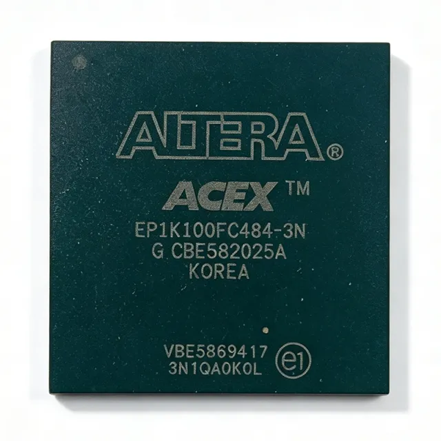
EP1K100FC484-3 - 100K Gates ACEX-1K FPGA | Altera | 484-FBGA
EP1K100FC484-3

EP1K100FC484-3 - 100K Gates ACEX-1K FPGA | Altera | 484-FBGA

The Altera (Intel) EP1K100FC484-3 is a member of the ACEX-1K family of low-cost, 2.5V SRAM-based FPGAs, providing 100,000 system gates, 4,992 logic elements (LEs), and 49,152 RAM bits in a 484-ball FineLine BGA (FC) package. Built on a 0.18 µm CMOS process with a 2.5V core, it is designed for system-on-a-programmable-chip (SOPC) integration in cost-sensitive designs. The device includes 333 user I/O pins and 624 LABs/CLBs, supporting densities up to 257,000 equivalent gates for complex digital designs. An FPGA (Field Programmable Gate Array) is a semiconductor device containing programmable logic blocks, interconnect, and I/O that can be configured by the customer after manufacture. FPGAs sit in the programmable logic category between fixed-function ASICs and general-purpose processors: they offer hardware-level parallelism and deterministic timing without the NRE cost of an ASIC. The ACEX-1K family specifically targets cost-sensitive, medium-density applications where designers need 10K-100K gates with embedded memory and PLL support, falling into the broader taxonomy: FPGA → programmable logic → programmable device → digital IC → semiconductor. Key features of the EP1K100FC484-3 include an internal configuration of 4,992 logic elements organized into 624 LABs, 12 embedded array blocks (EABs) for dual-port RAM/ROM, up to 49,152 bits of on-chip RAM, six clock input pins and four dedicated clock outputs, plus multi-volt I/O support for 2.5V, 3.3V, and 5V interfacing via dedicated VCCIO banks. The device also integrates a robust embedded array block architecture for efficient memory and specialized logic functions, and supports in-system programmability through the serial configuration scheme. Architecturally, the EP1K100FC484-3 uses an enhanced embedded array that combines dedicated dual-port RAM blocks (EABs) with fine-grained logic elements (LEs). Each EAB can be configured as 4,096 bits of RAM (with parity) or 2048 bits of true dual-port RAM, while each LE contains a 4-input LUT, a programmable register, and a carry chain for fast arithmetic. The FC484 package is part of Altera's SameFrame migration path with other FineLine BGA packages, allowing drop-in compatibility across density points within the family. Typical applications include telecommunications line cards, industrial control systems, consumer electronics with custom glue logic, low-volume prototyping for ASIC replacement, and embedded DSP preprocessing. The wide I/O count and embedded RAM make it suitable for bus interfacing, FIFO buffering, and state-machine-heavy control logic. The 484-FBGA package is suitable for high-density designs where signal integrity and board space are priorities. Design consideration: the EP1K100FC484-3 is an older 2.5V core device requiring level shifters to interface with modern 1.8V or 1.2V logic. Designers should also plan for an external configuration PROM (such as EPC2 or EPC8) or a microprocessor-driven configuration scheme, as SRAM-based FPGAs lose their configuration on power-down. The FC484 BGA footprint is the largest in the ACEX-1K family and should be matched against PCB manufacturing capability. This page synthesizes distributor availability data, drop-in compatible family members, and practical design notes that complement the official Altera ACEX-1K datasheet for sourcing and design-in decisions.

询价 联系我们
EP1K100FC484-3N - 100K-Gate ACEX 1K FPGA, 484-BGA | Intel
EP1K100FC484-3N

EP1K100FC484-3N - 100K-Gate ACEX 1K FPGA, 484-BGA | Intel

The Intel (formerly Altera) EP1K100FC484-3N is a 100,000-gate ACEX 1K family Field-Programmable Gate Array (FPGA) built on a 2.5V, 0.22 µm CMOS process, packaged in a 484-ball FineLine BGA (FBGA) and offering 333 user I/Os, 4,992 logic elements, 49,152 RAM bits, and a -3 speed grade with internal operating frequencies up to 200 MHz. The device combines a 4-input look-up-table (LUT) logic fabric with embedded array blocks (EABs) that implement RAM, ROM, dual-port RAM, or first-in first-out (FIFO) memory without external components. An FPGA (Field-Programmable Gate Array) is a programmable logic device that lets engineers implement arbitrary digital logic, signal-processing datapaths, glue logic, and embedded memory on a single chip after PCB fabrication. In the broader hierarchy, an FPGA sits above simple PAL/GAL SPLDs, above CPLDs, and below ASICs - it occupies the high-density, high-flexibility tier of programmable logic. The ACEX 1K family was Altera's first low-cost, die-efficient architecture that paired LUT-based logic with embedded memory, targeting system-on-a-programmable-chip (SOPC) designs. Key features include 624 logic array blocks (LABs), 12 EABs providing 49,152 bits of embedded memory, multiVolt I/O support for interfacing with 2.5V, 3.3V, and 5V systems, JTAG-based IEEE 1149.1 boundary-scan test, in-system programmability via the passive serial configuration scheme, and a dedicated configuration circuitry. The 484-ball FBGA package supports 333 user I/O pins - among the highest in the ACEX 1K family - enabling wide parallel buses, multiple communication interfaces, and address/data multiplexing for external memory or bus peripherals. Typical applications span telecommunications line cards, industrial control and factory automation, glue logic and bus bridging, glue-logic replacement of discrete 74-series logic, DSP pre/post-processing, and legacy ASIC prototyping. The combination of 100K ASIC gates of logic, dual-port RAM, and a 200 MHz internal fabric makes the EP1K100FC484-3N a practical choice for cost-sensitive volume production where an ASIC is not yet economical. When designing with the EP1K100FC484-3N, plan the I/O bank voltage assignments early because the device supports 2.5V, 3.3V, and 5V interfaces through multiVolt I/O but requires careful reference-voltage planning. The configuration scheme (PS, JTAG, or PPA) must be selected before PCB layout, and decoupling capacitors must be placed within 100 mils of every VCCINT and VCCIO pin. This page consolidates distributor pricing, same-brand drop-in equivalents, and ACEX 1K design considerations not available on a single manufacturer datasheet page, giving engineers a one-stop reference for sourcing and selecting this legacy FPGA.

USD $65.10 联系我们
EP1K100FC4842N - ACEX-1K 100K Gate FPGA, 484-BBGA | Altera
EP1K100FC4842N

EP1K100FC4842N - ACEX-1K 100K Gate FPGA, 484-BBGA | Altera

The Altera (Intel) EP1K100FC4842N is a member of the ACEX-1K programmable logic device family, providing low-cost system-on-a-programmable-chip (SOPC) integration in a single 484-ball BGA package. It features 100,000 typical gates, 49,152 bits of embedded array (EAB) memory, 4,992 logic elements, and 333 user I/O pins. The device operates from a 2.5V core supply with the "-2" speed grade, making it suitable for cost-sensitive high-volume designs. A Field-Programmable Gate Array (FPGA) is a semiconductor device built around a matrix of configurable logic blocks (CLBs), programmable interconnects, and I/O cells that allow the device to be reconfigured post-manufacturing for almost any digital function. FPGAs sit between general-purpose microcontrollers and fixed-function ASICs in the programmable logic hierarchy: gate array -> programmable logic device (PLD) -> complex PLD (CPLD) -> field-programmable gate array (FPGA) -> SoC FPGA. They offer hardware-level parallelism, deterministic timing, and rapid design iteration through HDL-based synthesis. Key features of the EP1K100FC4842N include 12 embedded array blocks (EABs) providing dual-port RAM up to 49152 bits total, tristate buffers per LAB for bus-oriented applications, multi-volt I/O support for 2.5V, 3.3V, and 5.0V mixed-voltage interfaces, JTAG-compliant boundary-scan testing (IEEE 1149.1), and built-in PCI compliance at 66 MHz. The device supports up to 49,152 RAM bits of true dual-port memory with byte enables, parity checking, and shift-register mode. The EP1K100FC4842N uses a SRAM-based Look-Up Table (LUT) architecture with a 0.18 µm CMOS process and 4-input LUTs, achieving density efficiency at low cost. Its continuous routing architecture uses direct-drive, fast-path connections for predictable timing closure. The "-2" speed grade denotes the second-fastest bin in the family, balancing Fmax and price for mainstream logic designs. Typical applications include PCI bus interfaces, bus bridges, DSP datapath acceleration, telecommunications line cards, industrial control, and embedded control blocks in copiers, network switches, and routers. Multi-volt I/O makes the part especially useful as a glue-logic bridge between 5V legacy ASICs and 3.3V processors. When designing with this device, plan for a 2.5V regulated core supply and separate VCCIO rails per I/O bank. The 484-BBGA package requires careful PCB stack-up and BGA escape routing. Use the Altera Quartus development suite for synthesis, place-and-route, and timing analysis. This page synthesizes distributor stock signals, drop-in pin-compatible ACEX-1K variants, and practical design notes not aggregated in the original ACEX-1K datasheet (Altera ACEX-1K Programmable Logic Device Family Data Sheet).

询价 联系我们
EP1K100FI256-2 - 100K Gate ACEX 1K FPGA, 256-BGA | Intel / Altera
EP1K100FI256-2

EP1K100FI256-2 - 100K Gate ACEX 1K FPGA, 256-BGA | Intel / Altera

The Intel (formerly Altera) EP1K100FI256-2 is an ACEX 1K family Field Programmable Gate Array (FPGA) delivering 100,000 system gates with 4,992 logic elements in a 256-ball FineLine BGA package. Per the manufacturer datasheet, the device integrates a look-up table (LUT)-based logic fabric with embedded array blocks (EABs) and is fabricated on a 2.5 V CMOS process supporting maximum operating frequencies up to 250 MHz. The "-2" speed grade designates a mid-range performance bin between the -1 (slower) and -3 (faster) ACEX 1K variants. A Field Programmable Gate Array (FPGA) is a type of programmable logic device (PLD) that combines configurable logic blocks, programmable interconnect, and I/O cells on a single die. Within the broader semiconductor taxonomy, FPGAs belong to programmable logic -> logic ICs -> integrated circuits. The ACEX 1K family occupies the low-cost system-on-a-programmable-chip (SOPC) tier of the Altera/Intel portfolio, combining LUT logic with EAB memory for efficient megafunction implementation such as FIFO buffers, RAM blocks, and specialized I/O functions. Key features of the EP1K100FI256-2 include 49,152 bits of embedded memory distributed across EABs, 186 user I/Os supporting multiple I/O standards, 2.5 V core supply with 3.3 V tolerant I/O, and in-system programmability via IEEE 1149.1 JTAG and Altera-specific configuration schemes. The device supports dual-port EAB memory and includes built-in clock management for synchronous design implementation. The architecture combines a die-efficient LUT fabric with EABs that can be configured as dual-port RAM, ROM, or specialized logic functions, providing an optimal balance between logic density and on-chip memory. The 0.22 µm CMOS process delivers predictable timing closure suitable for glue-logic, bus interfacing, and protocol bridging applications in cost-sensitive industrial and communications equipment. Typical applications include industrial control glue logic, communications protocol bridging, peripheral bus interfacing (PCI, ISA, UART bridges), low-density DSP preprocessing, and legacy system modernization. The 256-FBGA package supports compact board layouts while exposing the full 186 user I/O count for high-pin-count bridging scenarios. When designing with this device, verify Quartus or MAX+PLUS II support for the ACEX 1K family, as Intel has formally discontinued new ACEX 1K design entries in modern toolchains. The "FI" package code indicates industrial temperature grade (-40 °C to +85 °C) suitable for harsh-environment deployments. This page synthesizes distributor pricing, drop-in alternatives from the same ACEX 1K family, and practical design notes for legacy FPGA migration not found in the original manufacturer datasheet.

询价 联系我们