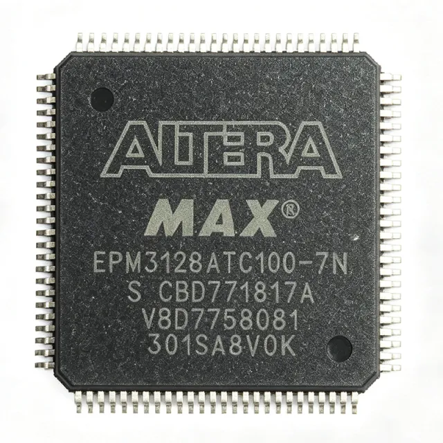
EPM3064ATI100-10N
EPM3064ATI100-10N - MAX 3000A CPLD, 64-Macrocell, 100-TQFP | Altera
The Intel (formerly Altera) EPM3064ATI100-10N is a member of the MAX 3000A family of Complex Programmable Logic Devices (CPLDs) fabricated on a 3.3-V CMOS EEPROM process. The device integrates 1,250 usable gates, 64 macrocells, and 66 user I/O pins in a 100-pin TQFP (industrial, -10 speed grade) package, with a worst-case pin-to-pin propagation delay of 10 ns and internal counter frequencies reaching 227.3 MHz.
What is a CPLD? A Complex Programmable Logic Device is a non-volatile programmable logic IC that sits in the product hierarchy below FPGAs but above simple PAL/GAL devices. CPLDs combine an EEPROM (or flash) configuration memory, an AND/OR logic plane, and a wide macrocell fabric, giving deterministic timing, instant-on behavior (no external boot PROM required), and high-drive I/O suitable for bus interfacing, glue logic, and state-machine decoding. The MAX 3000A family is the 3.3-V extension of Altera's classic MAX architecture, succeeding the 5-V MAX 7000 family and targeting cost-sensitive industrial and consumer glue-logic applications.
Key features of the EPM3064ATI100-10N include in-system programmability via the built-in IEEE Std. 1149.1 JTAG interface, MultiVolt I/O supporting 2.5 V/3.3 V/5 V mixed-voltage interfacing, PCI-SIG compliance (Revision 2.2) at -4/-5/-6/-7/-10 speed grades, programmable power saving per macrocell, and a JTAG-based boundary-scan test interface. The EEPROM cells retain configuration for more than 20 years and are reprogrammable in-circuit, eliminating the need for an external boot PROM and supporting rapid prototyping and field upgrades.
Architecturally, the device consists of four Logic Array Blocks (LABs), each containing 16 macrocells, connected via a programmable interconnect array (PIA). The PIA routes up to 36 signals to each LAB, while each macrocell combines a programmable AND/OR array with a flip-flop and I/O control block. The JTAG port (TCK, TMS, TDI, TDO) supports ISP and complies with the IEEE 1149.1 boundary-scan standard for board-level test access.
Typical applications include bus and address decoding in industrial controllers, glue-logic integration on PC/104 and embedded SBC boards, state-machine and timer replacement, level translation between 3.3 V and 5 V domains, and PCI interface logic where deterministic -10 ns timing meets the PCI Local Bus Specification, Revision 2.2. The industrial operating range of -40 C to +85 C and in-system programmability make it well suited to factory-automation backplanes and telecom control cards.
A key design consideration is the JTAG chain topology: when multiple devices share TDI/TDO, ensure the JTAG chain order is consistent with the Quartus II / MAX+PLUS II programming file, and provision a TCK pull-down to avoid floating-clock states. For new designs, the MAX II family (e.g., EPM240T100) offers lower cost, lower power, and a 100-pin TQFP-compatible footprint migration path.
询价
联系我们