产品(39,000+)

PEX8712-CA80BC - 12-Lane PCIe Gen 3 Switch | Broadcom
PEX8712-CA80BC

PEX8712-CA80BC - 12-Lane PCIe Gen 3 Switch | Broadcom

The Broadcom PEX8712-CA80BC is a PCI Express switch integrated circuit designed for 12-lane, 3-port PCIe Gen 3 systems. It is identified in the product listings as a special-purpose interface or PCI Express switch IC and uses a 324-pin FCBGA package measuring 19 x 19 mm. Broadcom describes the PEX 8712 as an ExpressLane PCIe Gen 3 switch developed on 40 nm technology, with multi-host switching capability for connecting multiple hosts to their respective endpoints. A PCIe switch is an interface IC that sits between a host or root complex and multiple PCIe endpoints. It provides fan-out, non-blocking interconnection, and centralized switching for systems such as servers, storage equipment, communications platforms, and graphics systems. The PEX8712-CA80BC is intended for designs that require a wider PCIe lane count and multiple downstream connections while maintaining Gen 3 PCIe operation. The verified product information identifies the device as a 12-lane, 3-port PCI Express Gen 3 switch. The Broadcom product page also specifies a typical power of 3.5 W and identifies the integrated package as a 19 x 19 mm, 324-pin FCBGA. These characteristics make the device suitable for board-level infrastructure where a compact, high-density switch implementation is required. The target orderable designation PEX8712-CA80BC is associated with the Broadcom PEX 8712 family. The listings use the related notation PEX8712-CA80BC-G, while the requested product identifier is PEX8712-CA80BC. Package details, electrical limits, thermal resistance, reference clock requirements, lane-specific performance, and the complete pin assignment require confirmation from the manufacturer datasheet before schematic release. Typical implementation involves routing the host-facing PCIe lanes, endpoint-facing lanes, auxiliary power, reference clock, control signals, and configuration interfaces through a dense multilayer PCB. Because the device is supplied in an FCBGA package, careful escape routing, via-in-pad or microvia strategy, reference-plane continuity, power delivery, and thermal management are essential. The 3.5 W typical power figure also makes power budget and junction-temperature calculations a central part of system validation. For new designs, verify the exact ordering code, package ball map, electrical characteristics, firmware requirements, reference design, and supported platform configuration with Broadcom. For replacement evaluation, use the manufacturer cross-reference process or the Request a Quote form on this page to confirm availability and technical suitability rather than assuming that a different PCIe switch is pin-compatible.

询价 联系我们
PEX88096B0-DB - 96-Lane PCIe 4.0 Switch | Broadcom | Storage
PEX88096B0-DB

PEX88096B0-DB - 96-Lane PCIe 4.0 Switch | Broadcom | Storage

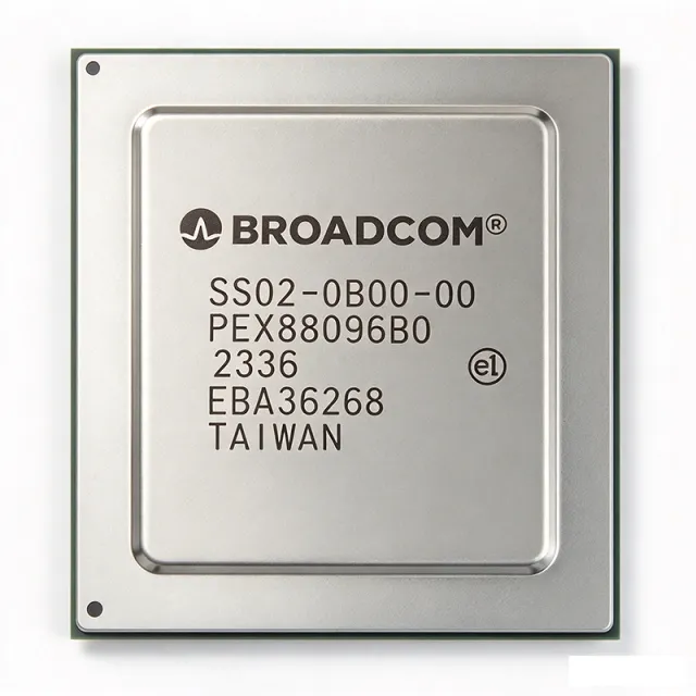
The Broadcom PEX88096B0-DB is a 96-lane PCI Express 4.0 managed switch from the PEX88000 series, delivered in a 1550-ball BGA package (37.5 x 42.5 mm) optimized for high-density storage and fabric applications. It provides 48 downstream ports and supports up to 98 solid-state drives through fan-out switching, while operating at the full PCIe 4.0 data rate of 16 GT/s per lane. A PCI Express (PCIe) switch is a high-speed serial fabric device that expands a single root-complex link into many endpoint links, enabling fan-out topologies in servers, storage arrays, and accelerator platforms. PCIe 4.0 is the fourth generation of the PCI Express standard, doubling the per-lane bandwidth of PCIe 3.0 to 16 GT/s. As a managed switch, the PEX88096 supports advanced features such as hot-plug, surprise-down recovery, dynamic port bifurcation, and Spread Spectrum Clocking (SSC) isolation, which are essential for enterprise storage and NVMe deployments. Key features include 96 total PCIe 4.0 lanes with 48 configurable downstream ports, integrated DMA and I/O virtualization support, hot-plug capability on every port, advanced error reporting (AER), and Broadcom's proprietary chip-link diagnostics. The device supports bifurcation configurations such as x4, x8, x16 per port and provides per-port signal-integrity tuning for reliable operation across long backplane traces. The 1550-ball BGA exposes a wide SERDES and sideband I/O complement suitable for adapter cards, backplanes, and custom ASIC/FPGA co-designs. Architecturally, the PEX88096B0 uses a non-blocking cut-through switching fabric with per-port credit-based flow control, multi-queue VC support, and a 32-bit MCU management interface. It is firmware-compatible with the broader PEX88000 family (including the PEX88064, PEX88080, and PEX88128), allowing OEMs to scale port count and lane count on a single software platform. Typical applications include NVMe SSD JBOD enclosures with 96+ drives, composable disaggregated storage fabrics, GPU/CPU accelerator pooling backplanes, hyperscale data-center storage tiers, and PCIe fan-out adapter cards. Both active and low-power standby states are exposed, making the device usable in dense thermal envelopes where chassis airflow is constrained. When designing with the PEX88096B0-DB, allocate at least six PCB layers with impedance-controlled 85 ohm differential SERDES routing, a dedicated reference clock distribution network with SSC support, and provide thermal management through the central heat-spreader pad. The on-chip microcontroller requires an external SPI flash for firmware boot.

USD $1,145.00 有现货
PEX90144 - 144-Lane PCIe Gen6 Switch | Broadcom | AI
PEX90144

PEX90144 - 144-Lane PCIe Gen6 Switch | Broadcom | AI

The Broadcom PEX90144 is a 144-lane PCI Express 6.0 packet switch built on a 5nm process, part of the Broadcom ExpressFabric PCIe switching family. It supports port widths of 2, 4, 8, or 16 lanes and delivers up to 256GB/s of bidirectional raw bandwidth per x16 port, with up to 9.2Tb/s of raw bandwidth achievable through the device in its largest configuration. A PCIe switch is a fabric device that expands a single root-complex PCI Express link into multiple downstream endpoints, aggregating GPU, NIC, storage controller, and accelerator traffic. In the system hierarchy, it sits between the host CPU root port and the endpoint tier, and is a core building block of modern data center interconnect fabrics alongside CPU PCIe controllers and retimers. Key differentiating features include hardware multi-host support for sharing the switch fabric across several hosts, an in-house Broadcom SerDes PHY exceeding 36dB of performance margin at Gen6 PAM-less NRZ data rates, and an embedded PCIe protocol analyzer for in-system debug without external interposer hardware. Turnkey fabric management software simplifies bring-up and topology configuration for large racks. Architecturally, the 5nm CMOS process integrates the SerDes, packet-routing fabric, and management engines on a single die, keeping per-lane power low while sustaining Gen6 64GT/s signaling. The device scales above its siblings, sitting as the widest device in Broadcom's published PCIe Gen6 switch lineup, which also includes 104-lane and 88-lane configurations. Typical applications include AI rack-scale connectivity between host CPUs and GPU accelerators, high-density server PCIe expansion chassis, composable and disaggregated infrastructure, and NVMe storage fabrics. It was publicly demonstrated integrated into a Dell PowerEdge XE7745-style PCIe board at SC25. Design consideration: at this bandwidth scale, signal-integrity planning for Gen6 64GT/s channels, substrate stack-up, and thermal design for the large BGA package are critical; consult the Broadcom PEX90000 series product brief for validated topologies. This page synthesizes distributor availability, family cross-references, and practical design guidance not found in the manufacturer datasheet.

询价 联系我们
PGA206UA - 5MHz FET-Input Programmable Gain In-Amp | TI
PGA206UA

PGA206UA - 5MHz FET-Input Programmable Gain In-Amp | TI

The Texas Instruments PGA206UA is a high-speed digitally programmable gain instrumentation amplifier (PGA) delivering a 5 MHz bandwidth, 100 pA maximum FET-input bias current, and digitally selectable gains of 1, 2, 4, and 8 V/V in a 16-pin SOIC (SOL-16) surface-mount package. A programmable gain instrumentation amplifier is a precision differential amplifier whose closed-loop gain is set by digital control inputs rather than external resistors. It sits within the amplifier hierarchy as an instrumentation amplifier -> precision op amp -> analog front-end (AFE) -> signal chain IC, combining a true three-architectural-input instrumentation amplifier front end with internally switched gain networks. PGAs are essential in data acquisition systems where a single amplifier must handle sensor signals spanning several orders of magnitude without manual range switching. Key features include fast settling to 0.01% after a gain change, +/-40V input protection that survives overrange faults common in industrial field wiring, and a low maximum offset voltage of 1.5 mV. The FET input stage keeps bias current at 100 pA max, preserving accuracy with high-impedance sources such as pH probes, photodiodes, and piezoelectric sensors. Technically, the PGA206 uses internally switched precision resistor networks controlled by two digital gain-select lines, a scheme the datasheet notes pairs naturally with an external logic latch to acquire gain data from a high-speed digital bus. Slew rate is 25 V/us and the supply range is +/-4.5V to +/-18V, allowing operation from standard +/-5V, +/-12V, or +/-15V analog rails. Operation is specified from -40C to +85C. Typical applications include multi-range data acquisition front ends, programmable sensor interfaces, test and measurement instrumentation, and dynamic signal conditioning where gain must change on-the-fly between measurements. Design consideration: total response time after a gain change equals the switching time plus the settling time to the new output voltage, so budget for settling in high-throughput scanning systems. This page synthesizes distributor pricing, drop-in alternatives, and practical design notes not found in the manufacturer datasheet.

询价 联系我们
PGA207UA - 5MHz Programmable Gain Instrumentation Amp | TI
PGA207UA

PGA207UA - 5MHz Programmable Gain Instrumentation Amp | TI

The Texas Instruments PGA207UA is a high-speed digitally programmable gain instrumentation amplifier offering a 5 MHz bandwidth, 100 pA maximum FET-input bias current, and digitally selectable gains of 1, 2, 5, and 10 V/V, housed in a 16-pin SOIC (SOL-16) surface-mount package. A programmable gain instrumentation amplifier (PGIA) is a precision differential amplifier whose closed-loop gain is set digitally rather than by external resistors. In the signal-chain hierarchy it sits between sensors and data converters, combining the true instrumentation-amplifier input stage (high common-mode rejection, balanced high-impedance inputs) with gain-switching logic, so a single ADC channel can resolve signals spanning several orders of magnitude. Key features of the PGA207 include two CMOS/TTL-compatible address lines for gain selection, analog inputs internally protected against overloads up to +/-40V even with the supplies off, and laser-trimmed offset voltage for low drift. A fast 0.01% settling specification allows the gain to be switched between conversions in high-throughput data-acquisition systems without dead time. Architecturally, the device uses a three-amplifier instrumentation topology with FET input transistors, giving negligible input bias current (100 pA max) for high-source-impedance sensors, a 25 V/us slew rate, and 18 nV/sqrt(Hz) input noise with 75 dB CMRR. Laser trimming at the Burr-Brown production line holds offset voltage to 1.5 mV max, preserving accuracy at the lowest gains. Typical applications include programmable data-acquisition front ends, dynamic signal ranges from PT100 sensors and strain-gauge bridges, test and measurement instrumentation, and industrial process-control analog front ends feeding 12- to 16-bit ADCs. When designing, remember the gain lines are logic-level inputs: tie them to clean CMOS/TTL levels and route away from the input traces. The +/-40V input protection removes the need for external clamp diodes in most industrial environments. This page consolidates distributor pricing, drop-in family alternatives, and engineering design guidance not found in a single manufacturer datasheet page.

询价 联系我们
PGA207UA/1K - 5MHz Programmable Gain In-Amp | Texas Instruments
PGA207UA/1K

PGA207UA/1K - 5MHz Programmable Gain In-Amp | Texas Instruments

The Texas Instruments PGA207UA/1K is a high-speed, digitally programmable gain instrumentation amplifier delivering gains of 1, 2, 5, and 10 V/V with a 5 MHz bandwidth, a FET input stage with 100 pA maximum bias current, and a 16-pin SOL-16 SOIC surface-mount package. A programmable gain instrumentation amplifier (PGIA) is a precision differential amplifier whose closed-loop gain is set digitally rather than by external resistors. Within the signal-chain hierarchy, it sits between raw transducers and ADCs as a front-end conditioning device, combining the high input impedance and CMRR of a true three-op-amp instrumentation amplifier with gain-switching logic that lets one device serve multiple transducer full-scale ranges. Key features of the PGA207UA/1K include digitally selectable gains (1, 2, 5, 10 V/V) via two CMOS/TTL-compatible address lines, fast settling to 0.01%, a FET input with maximum bias current of 100 pA, and internal input protection rated for plus/minus 40V overloads even with power supplies off. The device is laser-trimmed for low offset voltage (1.5 mV max) and low drift, eliminating manual calibration in most data acquisition designs. Technically, the PGA207 architecture uses a true instrumentation amplifier input stage whose gain is switched by the two digital address lines, so no external gain resistors are needed and gain accuracy is factory-determined. The 5 MHz bandwidth at higher gains supports multiplexed data acquisition channels, while the FET input minimizes loading on high-impedance sources such as photodiodes and piezoelectric sensors. Supply operation spans plus/minus 4.5V to plus/minus 18V, with a slew rate of approximately 25 V/us. Typical applications include multiplexed data acquisition front ends, programmable test and measurement signal conditioning, and industrial sensor interfaces where input channels of different amplitude must share one ADC. Fast settling allows channel-to-channel switching without long dead time, improving system throughput. Design consideration: ensure supply headroom within the plus/minus 4.5V to plus/minus 18V range and route the digital gain-select lines away from the high-impedance inputs to prevent digital noise coupling into the analog front end. This page synthesizes distributor pricing, drop-in family alternatives, comparison data, and practical design notes not found in the manufacturer datasheet.

询价 联系我们
PGA281 - Zero-Drift Programmable Gain Instrumentation Amplifier | TI
PGA281

PGA281 - Zero-Drift Programmable Gain Instrumentation Amplifier | TI

The PGA281 is a high-precision instrumentation amplifier from Texas Instruments featuring digitally-controllable gain and signal-integrity test capability. It uses proprietary autozeroing techniques to achieve low offset voltage, near-zero offset and gain drift, excellent linearity, and nearly no 1/f noise. The device is available in a 16-pin TSSOP package (PW) and operates over a wide supply range, making it suitable for precision sensor interfaces and data acquisition systems. An instrumentation amplifier (INA) is a type of differential amplifier that amplifies the difference between two input signals while rejecting common-mode voltages. It is characterized by high input impedance, high common-mode rejection ratio (CMRR), and low offset voltage. The PGA281 belongs to the family of programmable gain instrumentation amplifiers (PGIAs), which allow the gain to be set digitally or via external resistors, providing flexibility in signal conditioning chains. This category sits within the broader hierarchy of analog amplifiers, which are essential building blocks in electronic systems for signal conditioning and measurement. Key features of the PGA281 include gain programmable from G = 0.2 to 10,000 using an external resistor, fully differential outputs with integrated clamping, low offset voltage of 10 µV (typ) and 35 µV (max), low offset drift of 0.1 µV/°C (typ) and 0.3 µV/°C (max), and low input bias current of 5 pA (typ). These specifications make it ideal for high-accuracy applications where drift and noise are critical. The PGA281 employs a zero-drift architecture that continuously corrects offset and drift, achieving near-zero temperature coefficients. The integrated clamping circuitry protects the outputs from overvoltage conditions, enhancing system robustness. The device supports a wide supply range, typically ±5V, and provides rail-to-rail output swing, maximizing dynamic range. Typical applications include precision current sensing (10 µA to 100 mA), sensor signal conditioning for bridge sensors, thermocouple amplifiers, and data acquisition front-ends. Its low offset and drift make it suitable for medical instrumentation, industrial process control, and test and measurement equipment. When designing with the PGA281, ensure proper decoupling of the power supply pins and consider the thermal performance of the TSSOP package. The gain-setting resistor should be a precision resistor to maintain gain accuracy. The device's signal-integrity test capability allows for system-level diagnostics, which is valuable in safety-critical applications.

询价 联系我们
PGA309AIPWR - Programmable Sensor Conditioner | TI | 16-TSSOP
PGA309AIPWR

PGA309AIPWR - Programmable Sensor Conditioner | TI | 16-TSSOP

The PGA309AIPWR from Texas Instruments is a voltage output programmable analog signal conditioner designed specifically for resistive bridge sensors. It integrates a precision analog signal path with digital calibration capabilities, enabling correction of zero, span, zero drift, span drift, and sensor linearization errors. Housed in a 16-pin TSSOP (PW) package, this device operates over a temperature range of -40°C to +125°C, making it suitable for industrial and automotive environments. A programmable sensor conditioner is an integrated circuit that amplifies and calibrates the small differential output of a bridge sensor, such as a strain gauge or pressure sensor, converting it into a linear, temperature-compensated voltage output. It sits between the sensor and the ADC or microcontroller, forming a complete sensor signal chain. This category falls under sensor interface ICs within the broader analog signal processing domain. Key features include a programmable gain amplifier (PGA) with adjustable gain, a digital-to-analog converter (DAC) for offset and span calibration, and an internal temperature sensor for drift compensation. The device supports a supply voltage up to 5.5V and provides a ratiometric or absolute voltage output. Its digital interface allows in-system calibration via a two-wire serial interface, simplifying production trimming. The PGA309 employs a chopper-stabilized amplifier architecture to achieve low offset and drift, ensuring high accuracy over temperature. The integrated calibration engine uses look-up tables to linearize the sensor response, reducing the need for external components. This architecture provides a complete, factory-calibrated solution that minimizes assembly cost and improves yield. Typical applications include industrial pressure transmitters, automotive manifold absolute pressure (MAP) sensors, and precision weigh scales. The device's wide temperature range and programmable features make it ideal for harsh environments where sensor accuracy is critical. When designing with the PGA309AIPWR, ensure proper decoupling of the supply pins and careful layout of the analog input traces to minimize noise. The calibration coefficients should be stored in an external EEPROM, as the device does not have non-volatile memory on-chip.

询价 联系我们
PI2DBS212ZHEX - 2-Channel Broadband Switch | Diodes
PI2DBS212ZHEX

PI2DBS212ZHEX - 2-Channel Broadband Switch | Diodes

The Diodes Incorporated PI2DBS212ZHEX is a 2-channel differential broadband switch IC with a stated 1.2 V to 1.8 V single-supply range and a 28-pin TQFN package measuring 3.5 mm by 5.5 mm. It is categorized as a special-purpose analog switch and is intended for telecommunications signal routing. The verified distributor results also identify it as a dual 1:2 analog multiplexer, indicating that each channel can route a signal between multiple paths. An analog switch is a semiconductor-controlled routing element that connects or isolates circuit nodes with relatively low impedance in the selected state. In the broader hierarchy, this PI2DBS212ZHEX is a special-purpose analog switch, then an interface IC, then a semiconductor. Broadband switches are used where a signal must reach different downstream circuits with controlled insertion loss, isolation, and switching behavior. Their performance depends on supply voltage, signal amplitude, frequency, control logic, layout parasitics, and the impedance of the connected network. The PI2DBS212ZHEX is specified for single-supply operation from 1.2 V to 1.8 V. Two channels and differential broadband routing are its principal verified functional characteristics. The 28-TQFN package supports compact surface-mount layouts, while the exposed pad, where applicable, provides a thermal connection to the PCB. The available distributor snippets do not provide verified insertion loss, bandwidth, on-resistance, off-isolation, leakage, switching time, control thresholds, or absolute maximum ratings, so those values remain unavailable in this data set. Telecommunications equipment is the clearest fit because the manufacturer and DigiKey classify the device as a telecommunications switch. It may also be evaluated for broadband test paths, routing networks, and communication modules when its complete electrical limits satisfy the system requirements. The low 1.8 V upper supply limit is important: downstream circuitry must remain compatible with this range, and signal amplitudes must not exceed verified device limits that are not present in the supplied records. PCB implementation should follow the manufacturer pinout and land pattern once the official datasheet is obtained. Place power and ground connections directly to their assigned pins, keep high-frequency switched traces short, and minimize copper around sensitive routing nodes. Because exact pin names, control timing, and electrical characteristics are unavailable, a board should not be released for production until those details are verified against the official PI2DBS212 datasheet. This product record consolidates verified distributor identification, sourcing information, and design caveats while clearly separating known facts from missing technical data. It is intended to support early component selection, quotation requests, and engineering follow-up rather than replace the manufacturer datasheet or a completed signal-integrity evaluation.

询价 联系我们
PI2USB4122ZHEX - USB 3.2 Gen 1 4:1 Mux/DeMux Switch | Diodes Inc
PI2USB4122ZHEX

PI2USB4122ZHEX - USB 3.2 Gen 1 4:1 Mux/DeMux Switch | Diodes Inc

The Diodes Incorporated PI2USB4122ZHEX is a high-performance USB 3.2 Gen 1 (formerly USB 3.0) 4:1 mux/demux switch IC housed in a 42-TQFN (9x3.5 mm) package with an exposed thermal pad. The device supports four differential channels that can be routed between one USB Type-C/USB 3.0 port and four possible source/sink endpoints, enabling switching of SuperSpeed USB (5 Gbps) signals with minimal insertion loss and return loss across the full USB 3.2 Gen 1 frequency spectrum. A USB switch (also called a USB mux/demux or USB crossbar switch) is a high-speed analog multiplexer designed to route USB 2.0 and SuperSpeed USB signals between multiple physical connectors or controllers while preserving signal integrity. As a category, USB switches sit within the broader hierarchy of analog switches and multiplexers -> signal switches -> interface ICs -> semiconductors. They are essential building blocks in any system that must share limited USB ports among multiple functions (charging, data, audio, debug), and they sit electrically downstream of the USB PHY and upstream of the physical connector. PI2USB4122 is the second-generation Diodes Inc. offering in this category and operates from a single 1.8 V supply rail, simplifying integration into modern low-voltage SoCs. Key differentiating features include 5 Gbps SuperSpeed USB channel support, low 5 ohm typical on-resistance per channel, -3 dB bandwidth exceeding 2.5 GHz to preserve USB 3.2 Gen 1 eye margins, 1.8 V single-supply operation, and integrated sideband/USB 2.0 pass-through routing. The exposed thermal pad on the TQFN package keeps the die-to-ambient thermal resistance low enough for hot-plug events without derating. The PI2USB4122 uses a wide-bandwidth CMOS pass-gate architecture with adaptive biasing to maintain flat frequency response up to 2.5 GHz. Internal ESD protection exceeds 2 kV HBM on the high-speed data lines, reducing external TVS diode count. The control logic accepts standard GPIO inputs for channel selection, allowing direct connection to a USB Type-C port controller without an external I/O expander. Typical applications include USB Type-C port multiplexers in laptops, tablets and docking stations, smartphone fast-charge/data switching paths, USB 3.0 hubs with multiple upstream ports, and Thunderbolt/USB4 sideband routing. The exposed-pad TQFN package makes it suitable for both handheld and dock designs where PCB real estate is constrained. When designing with this part, note the NRND (Not Recommended for New Design) status - the family remains in production for existing platforms but new designs should evaluate the PI3USB4122 or PI3USB31432 successors. Decoupling must include a 0.1 uF X7R cap on VCC placed within 2 mm of the exposed pad, and the high-speed differential pairs require 85 ohm differential impedance with matched trace lengths within the data-sheet tolerance window. This page synthesizes distributor pricing across DigiKey, Mouser, Arrow and LCSC, drop-in alternative candidates from the same Diodes Inc. family, and practical design notes drawn from the manufacturer datasheet - information not aggregated on any single distributor site.

询价 联系我们
PI3DBS16213XEAEX - PCIe Gen 4 MUX 12GHz Switch | Diodes Inc
PI3DBS16213XEAEX

PI3DBS16213XEAEX - PCIe Gen 4 MUX 12GHz Switch | Diodes Inc

The Diodes Incorporated PI3DBS16213XEAEX is a 2-channel, 3:1 PCIe Gen 4 multiplexer/switch IC that routes high-speed differential signals between a single common port and three separate downstream paths, delivering up to 12 GHz of -3 dB bandwidth for next-generation server and add-in-card applications. Housed in a 24-pin X1QFN (2x4 mm) exposed-pad package, the device operates from a 3.3 V supply and is rated for the industrial -40 °C to +85 °C temperature range with bidirectional analog switching on each channel. Background Knowledge: A PCIe multiplexer (MUX) is a type of high-speed analog switch that belongs to the broader family of analog switches and multiplexers used in digital interface ICs. PCIe switches sit within the signal-integrity layer between a host CPU/chipset and peripheral endpoints, allowing designers to share a single PCIe lane across multiple downstream devices (such as SSDs, NICs, or riser connectors). They are commonly deployed in storage backplanes, GPU workstations, and server riser cards where lane routing flexibility is required without expanding the host's native PCIe fan-out. Key features of the PI3DBS16213 include 12 GHz bandwidth enabling PCIe Gen 4 (16 GT/s) signaling, two differential channels for 4-lane packet switching capability, low insertion loss for signal-integrity compliance, and bidirectional flow-through pin assignment that simplifies PCB routing on inner stripline layers. The X1QFN-24 (2x4 mm) package exposes a thermal pad that ties to the system ground plane for EMI shielding and thermal dissipation. Architecturally, the device uses a passive FET-based switching matrix with minimal parasitic capacitance, optimizing return-loss and crosstalk figures required for PCIe Gen 4 link-training sequences. Internal bias generation on each channel reduces the BOM by eliminating external DC blocking caps on many reference designs. Typical applications include PCIe Gen 4 server backplanes, NVMe SSD port multipliers on storage enclosures, GPU workstation riser cards, and any design that needs to switch PCIe lanes between two downstream partners without unplugging cables. The 3.3 V single-rail operation is compatible with mainstream server auxiliary rails. Design consideration: maintain a continuous reference (ground) plane under the X1QFN exposed pad to achieve the datasheet's signal-integrity targets; non-continuous flex would degrade return loss at the Nyquist frequency of PCIe Gen 4 (8 GHz fundamental). Source impedance should target 85 Ω differential with skew matched to within 5 ps per channel. This page synthesizes distributor pricing, drop-in-compatible alternatives, application guidance, and engineering design notes not consolidated in the manufacturer brief, giving procurement and design engineers a single decision-ready reference.

询价 联系我们
PI3DPX1202A1ZB - DP 1.2 Redriver, 5.4Gbps, 48-TQFN | Diodes Inc
PI3DPX1202A1ZB

PI3DPX1202A1ZB - DP 1.2 Redriver, 5.4Gbps, 48-TQFN | Diodes Inc

The Diodes Incorporated PI3DPX1202A1ZB is a low-power DisplayPort 1.2 redriver with integrated DDC/AUX channel switch, supplied in a 48-pin TQFN (7x7 mm) package. It supports all three DisplayPort 1.2 data rates - 1.62 Gbps (RBR), 2.7 Gbps (HBR) and 5.4 Gbps (HBR2) - and dual-mode DisplayPort (DP++) with TMDS clock frequencies up to 340 MHz, enabling HDMI interoperability through a passive adapter. The device presents a 1-channel high-speed signal path with internal 50 ohm input pull-downs, configurable output level and pre-emphasis, and an Aux Listener that supports link training. What is a DisplayPort redriver? A redriver (also called a signal repeater or retimer-less repeater) is a linear equalizer placed in series with a high-speed serial link. Unlike a retimer it does not add a clock-data-recovery block; instead it compensates for channel loss with adjustable input equalization and output de-emphasis, then re-drives the signal to restore eye-diagram margin. Redrivers sit between a source (GPU, SoC) and a sink (monitor, dongle) and belong to the signal-conditioning family of interface ICs alongside retimers, crosspoint switches and redrivers for USB, PCIe and HDMI. Key features include an ultra-low-power design (136 mA typical at 400 mVpp swing, 0 dB setting), pin-to-pin compatibility with the prior-generation PI3EQXDP1201, dual-mode (DP++/TMDS) input and output, integrated DDC/AUX channel switch, and selectable output level and pre-emphasis through external configuration. The 48-TQFN package combines an exposed thermal pad with a compact 7x7 mm body to fit space-constrained docking stations and embedded DisplayPort designs. The PI3DPX1202A1ZB uses Pericom's (now Diodes) proven linear-redriver architecture, with adaptive or fixed equalization that recovers the high-frequency content attenuated by PCB traces, cable assemblies, and connector transitions. This allows system designers to extend usable cable length, route signals through denser board layouts, or pass strict DisplayPort 1.2 compliance eye-mask tests at the connector. Typical applications include notebook docking stations, DisplayPort 1.2 graphics cards, motherboards with embedded DP outputs, DP-to-HDMI adapters (DP++/TMDS), 4K UltraHD monitors, and Thunderbolt accessory boards. The 5.4 Gbps HBR2 rate supports 4K@60 Hz (3840x2160) color-depth-rich video streams. When designing with this part, place the device as close as practical to the source connector to maximize the recovered signal integrity budget on the far end. Use the AC-coupling capacitors specified in the datasheet, follow the recommended reference-resistor values for the desired output swing, and respect the thermal-pad soldering guidelines for the 48-TQFN package. This page synthesizes distributor stock, same-family Diodes alternatives, and PCB-layout guidance beyond the manufacturer datasheet, with information gain not duplicated on DigiKey or Mouser product pages.

询价 联系我们
PI3DPX1202A1ZBE - 5.4Gbps DisplayPort 1.2 Redriver | Diodes Inc
PI3DPX1202A1ZBE

PI3DPX1202A1ZBE - 5.4Gbps DisplayPort 1.2 Redriver | Diodes Inc

The Diodes Incorporated PI3DPX1202A1ZBE is a low-power DisplayPort 1.2 redriver with integrated DDC/AUX channel switch, supplied in a 48-pin TQFN (V-QFN7070-48, 7x7 mm) package with exposed thermal pad. The device supports one channel at up to 5.4 Gbps data rate per lane, making it suitable for DisplayPort 1.2 (HBR2) source-side and sink-side signal conditioning. Per the Diodes datasheet, the PI3DPX1202A1 offers signal buffering/redriver functionality with integrated DDC/AUX multiplexer switching between source and sink. A signal buffer/redriver is a linear or adaptive repeater placed in series with a high-speed serial channel to compensate for channel loss caused by PCB traces, connectors, cables, or inter-symbol interference. It restores signal amplitude and rise/fall times without re-timing the data (a redriver is protocol-transparent), which is critical for DisplayPort, HDMI, USB 3.0, and PCIe Gen2/Gen3 links where budgets may be exceeded by the physical medium. Within the broader component taxonomy, a redriver sits below retimers (which recover clock/data) and above simple repeaters, and it belongs to the Interface ICs > Signal Buffers, Repeaters family of mixed-signal analog conditioning products. Key features include 5.4 Gbps per-lane support (DisplayPort HBR2), adaptive equalization to compensate for frequency-dependent channel loss, transmit de-emphasis to reduce inter-symbol interference at the source, integrated DDC/AUX switch for source/sink routing, low standby current, and 3.3 V single-supply operation. The TQFN-48 (7x7 mm) package with exposed pad provides a low thermal resistance path for surface-mount designs. Internally, the redriver combines a CTLE-style adaptive equalizer at each input with a fixed or selectable de-emphasis driver at each output, plus auxiliary logic for DDC/AUX channel switching. The equalizer extends the usable channel length at HBR2 (5.4 Gbps) where 28 AWG cable losses exceed 10 dB at the Nyquist frequency. The DDC/AUX switch supports bidirectional auxiliary and EDID transactions without an external mux. Typical applications include notebook docking stations, monitor input panels, DisplayPort dongles and adapters, embedded display boards, video capture cards, and any compact DisplayPort source/sink where PCB trace or cable length exceeds the native 8-10 dB loss budget at HBR2 rates. When designing with this part, place it within 4 inches of the DisplayPort connector; provide a solid 3.3 V decoupling network (10 uF bulk + 0.1 uF/0.01 uF high-frequency) at VCC; and route the high-speed TX/RX pairs with 100 ohm differential impedance and length matching within 5 mils per pair. This page synthesizes distributor pricing, drop-in same-package alternatives from the Diodes DisplayPort redriver family, DDC/AUX mux companion parts, and practical PCB layout notes not aggregated in the manufacturer datasheet.

询价 联系我们
PI3USB102GZLEX - USB 2.0 2:1 Switch with 5V Protection | Diodes Inc
PI3USB102GZLEX

PI3USB102GZLEX - USB 2.0 2:1 Switch with 5V Protection | Diodes Inc

The Diodes Incorporated PI3USB102GZLEX is a high-performance USB 2.0 high-speed switch configured as a single differential channel 2:1 multiplexer/demultiplexer, packaged in a 10-pin TQFN (1.3x1.6 mm) with an exposed thermal pad. It supports USB 2.0 high-speed (480 Mbps) signaling, offers low on-resistance (5 ohm max), a 1 GHz -3 dB bandwidth, and integrated 5V over-voltage protection on Y+/Y- pins per USB 2.0 specification, allowing all I/O pins to withstand Vbus shorts (5V +/- 10%) whether the chip is powered on or off. A USB switch is a specialized analog multiplexer designed to route USB 2.0 differential pairs between two physical ports or between a single port and a downstream controller. It belongs to the broader family of analog switches and multiplexers, which sit under interface ICs in the semiconductor taxonomy. These parts are critical in systems where one USB physical-layer transceiver must service multiple connectors, OTG roles, USB Type-C role swaps, dock/multi-connector designs, or test-mode path selection. By isolating one data path while activating another, the switch lets one SoC PHY serve two USB connectors without contention. Key differentiating features include very low bit-to-bit skew, high channel-to-channel noise isolation, flow-through pinout for simplified PCB routing, and an improved Ioff voltage range that reduces leakage when VCC is removed. Bidirectional operation means it supports both host-side and device-side roles equally well, and it operates across the -40C to +85C industrial temperature range. The 10-TQFN (1.3x1.6) footprint measures only 2.08 mm^2, enabling it to fit comfortably inside USB connector shields, Type-C mid-mount boards, and dongle-class products. Typical applications for the PI3USB102GZLEX span consumer tablets, notebooks, dock stations, USB Type-C adapters, OTG phones, and any system that needs to share one USB 2.0 PHY between two physical ports. Inside a tablet, for example, it sits between the SoC's USB pins and the system micro-USB or Type-C connector, providing 5V Vbus short protection for the SoC's USB lines. The part can also multiplex between an internal USB header and an externally accessible connector for service-mode diagnostics or docking. When designing with the PI3USB102GZLEX, place the device adjacent to the USB connector so the 5V Vbus short protection works as close to the system boundary as possible. Use a 100 nF decoupling capacitor close to VCC, and follow the USB 2.0 differential pair impedance target of 90 ohm differential. When the chip is powered down, signal leakage through the switch is dominated by Ioff, so confirm this does not exceed downstream PHY leakage budgets. This page synthesizes distributor pricing, drop-in same-package alternatives, and practical PCB design considerations - information that goes beyond what is found in the manufacturer datasheet alone.

询价 联系我们
PI3VST01UE - VGA HPD Signal Generator | MSOP-8 | Diodes
PI3VST01UE

PI3VST01UE - VGA HPD Signal Generator | MSOP-8 | Diodes

The Diodes Incorporated (formerly Pericom) PI3VST01UE is a single-channel VGA Hot Plug Detect (HPD) signal generator IC housed in an 8-pin MSOP (Mini Small Outline Package). The device generates a buffered HPD logic signal used in legacy VGA connectors, supporting DisplayPort-to-VGA adapters, docking stations, and monitor-side hot-plug detection circuits where a clean, low-jitter logic-level assertion is required. Key features include a wide 3.0 V to 5.5 V single-rail supply range, CMOS/TTL-compatible HPD output, low quiescent current draw suitable for always-on bias rails, and an integrated pull-up on the HPD output pin per the VESA-recommended 1 kohm impedance. The MSOP-8 surface-mount package is footprint-compatible with standard industry pinouts and supports automated PCB assembly. The PI3VST01UE is a specialized analog mixed-signal interface IC belonging to the analog switch / special-purpose switch family (also classifiable as a video interface switch). Within the broader component taxonomy it sits under interface ICs, video ICs sub-category, semiconductor -> integrated circuit -> analog mixed-signal IC -> HPD signal generator. Its function is to provide electrical buffering and level translation of the HPD logic signal that source devices use to detect cable presence on VGA/DisplayPort output chains. Typical applications include DisplayPort-to-VGA adapters, video docking stations, monitor-side cable-presence detection on VGA inputs, KVM switches that must expose HPD to a graphics source, and legacy graphics cards that lack a native HPD output stage. It is also used in industrial video distribution equipment where hot-plug events must be regenerated cleanly to avoid host GPU re-enumeration glitches. When designing with this device, observe standard ESD precautions on the VGA DDC/HPD lines and decouple VCC with at least a 0.1 uF ceramic capacitor placed within 5 mm of the supply pin. The exposed pad on the MSOP-8 should be soldered to the PCB ground plane for thermal performance and pin-1 reference accuracy. This page synthesizes distributor pricing (DigiKey, Mouser, Octopart), package-level cross-references, drop-in alternatives, and PCB-level design notes into a single reference that is not duplicated on the manufacturer datasheet.

询价 联系我们
PI4IOE5V96248ZLEX - 48-bit I2C I/O Expander 56-TQFN | Diodes Inc
PI4IOE5V96248ZLEX

PI4IOE5V96248ZLEX - 48-bit I2C I/O Expander 56-TQFN | Diodes Inc

The Diodes Incorporated PI4IOE5V96248ZLEX is a 48-bit I2C-bus I/O expander organized as 6 banks of 8-bit quasi-bidirectional I/O, packaged in a 56-pin TQFN (7x7 mm) with an exposed thermal pad. It operates from a 2.3 V to 5.5 V supply, supports a 1 MHz I2C (Fast-mode Plus) interface, and provides an open-drain interrupt output plus a hardware reset pin for cascading and address expansion. An I2C I/O expander is a digital IC that multiplies the limited GPIO resources of a host microcontroller by exposing additional general-purpose input/output pins addressable over the two-wire I2C serial bus. In the broader component hierarchy, this places the device within the interface IC category (I/O expanders), itself a subclass of digital logic and bus-interface semiconductors that sit between a controller and peripheral signals. The PI4IOE5V96248 specifically targets MCUs whose GPIO count is the limiting factor for keypads, switches, LEDs and other human-machine interfaces. Key features include built-in LED driver capability with selectable drive strength (25 mA / 30 mA per pin), 250 nA typical standby current, push-pull and open-drain output modes, hardware reset, and cascading capability through user-configurable I2C addresses. The 56-TQFN exposed-pad package provides a low thermal resistance path that sustains continuous high-current LED drive without derating. The device integrates 5 V tolerant I/O on a 2.3 V-5.5 V supply, allowing direct interface to 3.3 V and 5 V rails without level shifters. Internally the chip implements six 8-bit I/O banks (P0..P5), each with independent control registers for direction, pull-up enable, output value, and interrupt-on-change masking. The interrupt output aggregates any unmasked change across the 48 pins and signals the host, while the reset pin simplifies multi-chip synchronization and cascaded configurations. The 1 MHz I2C clock and cascading address expansion make it suitable for very large GPIO fanouts in industrial control panels. Typical applications include industrial keypads and control panels, multi-LED status indicators, white goods human-machine interfaces, point-of-sale terminals, and any MCU-limited system requiring 48 or more general-purpose I/O lines. The integrated LED driver also makes it a strong fit for RGB lighting arrays that otherwise occupy multiple MCU pins with software PWM. When designing with this part, route the 56-TQFN exposed pad to a contiguous ground copper pour for both thermal dissipation and low-impedance return. The I2C pull-ups must be sized for the 1 MHz Fast-mode Plus clock; values in the 1 kOhm to 2.2 kOhm range are typical for 3.3 V and 5 V rails. Multiple PI4IOE5V96248 devices may share the bus by setting their A0/A1/A2 address straps to unique values, expanding the system to 192 I/O or more without any firmware change to the bus protocol layer. This page synthesizes distributor pricing, drop-in alternatives, and practical I2C expander design notes not found in the manufacturer datasheet alone.

询价 联系我们
PI5USB31213 - USB Type-C DRP Controller 10Gbps | Diodes Inc.
PI5USB31213

PI5USB31213 - USB Type-C DRP Controller 10Gbps | Diodes Inc.

The Diodes Incorporated PI5USB31213 is a USB Type-C Dual Role Port (DRP) controller with integrated 2:1 USB 3.2 Gen 2 differential mux switches supporting 10Gbps SuperSpeed data rates, housed in a 24-pin X1-QFN (2x4 mm) package. It supports both pin control and I2C control based on the ADDR pin setting. A USB Type-C port controller manages configuration channel (CC) logic, connector orientation detection, and power role negotiation between host, device, and dual-role ports. Within the power management and interface IC hierarchy, DRP controllers bridge the USB Type-C connector and the system USB controller, automatically configuring port roles and flipping SuperSpeed differential pairs for either plug orientation. Key features include compliance with USB Type-C Specification 1.1, dual differential channel 10Gbps mux/deMux switching, automatic port orientation configuration through CC detection, and VCONN sourcing to power active cables and accessories. In host mode the device monitors the ID pin for connector status and offers default current mode to power attached accessories. The PI5USB31213 supports host-mode, device-mode, and dual-role-mode operation selected via the PORT pin, and integrates the USB controller interface and Type-C connector logic in one die, reducing external component count compared to a discrete mux plus separate CC controller. The 5V VCONN sourcing capability eliminates an external VCONN supply for powered cables. Typical applications include smartphones and tablets with USB Type-C connectors, laptops and notebooks requiring dual-role ports, docking stations, and desktop motherboards implementing USB 3.2 Gen 2 front-panel ports where a 10Gbps switchable mux is required. Design considerations: note that the PI5USB31213 is classified NRND (Not Recommended for New Designs) by Diodes Incorporated; new designs should use the actively promoted PI5USB31213A, which shares the same feature set including USB 3.2 Gen 2 10Gbps switching and Type-C 1.1 support. Verify SuperSpeed channel insertion loss budget over the mux at 10Gbps in the layout. This page synthesizes distributor pricing from LCSC, DigiKey, and Mouser, drop-in alternative analysis, and lifecycle guidance not found in the manufacturer datasheet, as of 2026-10-19.

询价 联系我们
PI6C557-03AQE - PCIe 2.0 Spread Spectrum Clock Generator | Diodes Inc
PI6C557-03AQE

PI6C557-03AQE - PCIe 2.0 Spread Spectrum Clock Generator | Diodes Inc

The Diodes Incorporated PI6C557-03AQE is a spread-spectrum clock generator compliant with PCI Express 2.0 and Ethernet timing requirements, packaged in a 16-pin QSOP (also referenced as 16-SSOP by some listings). The part accepts a 25 MHz fundamental-mode crystal reference and produces two pairs of differential HCSL outputs at user-selectable frequencies of 25 MHz, 100 MHz, 125 MHz, and 200 MHz. Spread-spectrum modulation is applied through a proprietary PLL architecture to substantially reduce electromagnetic interference (EMI) on the system reference clock. A spread-spectrum clock generator is a timing device that intentionally modulates the output frequency around a center value at a low modulation rate. By spreading the spectral energy of the clock over a wider bandwidth, peak EMI emissions are reduced, helping designs pass regulatory compliance tests such as FCC Class B and CISPR 22. Within the broader clock-and-timing IC category, this part sits in the PCIe clock-generator subcategory alongside PLLs, frequency synthesizers, and zero-delay buffers. Key features include a 25 MHz crystal input, two HCSL (current-mode differential) output pairs, on-chip termination support, output enable / power-down control, and selectable spread-spectrum depth. HCSL is the signaling standard required by PCIe 2.0/3.0 reference clocks and is also used in mainstream Ethernet PHYs. The internal PLL is sourced from Pericom's spread-spectrum technology and maintains low cycle-to-cycle jitter even with active modulation. Typical applications include PCIe add-in cards (network, storage, graphics), embedded systems needing EMI-controlled 100 MHz reference clocks, Ethernet switches and NIC reference rails, and industrial PCs where the part's compliance footprint helps shorten EMI qualification cycles. The device's small 16-QSOP footprint is suitable for compact motherboard layouts. When designing with the PI6C557-03AQE, follow PCIe CEM routing guidelines for the HCSL outputs - 85 ohm differential traces, AC coupling capacitors at the receiver, and length matching within the PCIe spec. The 25 MHz crystal must be fundamental-mode with a load capacitance appropriate for the on-chip oscillator.

询价 联系我们
PI6C557-03LEX - 200MHz PCIe Clock Generator | Diodes
PI6C557-03LEX

PI6C557-03LEX - 200MHz PCIe Clock Generator | Diodes

The Diodes Incorporated PI6C557-03LEX is a 200 MHz PCI Express and Ethernet clock generator with two differential HCSL outputs, supplied in a 16-TSSOP package. It accepts a 25 MHz crystal input and uses Pericom PLL techniques to generate selectable 25 MHz, 100 MHz, 125 MHz, and 200 MHz clock frequencies. The verified distributor data identifies a 3.3 V supply, a -40°C to +85°C operating range, and two clock outputs. Its clock-generation and spread-spectrum functions position it within the clock and timing IC category as a phase-locked-loop-based timing device for high-speed digital systems. A clock generator produces reference and data-rate clocks for digital circuits that require stable timing, phase control, and predictable edge placement. In a PCI Express system, a spread-spectrum clock can reduce electromagnetic-interference peaks by distributing clock energy over a frequency band. The PI6C557-03 family is designed for PCI Express and Ethernet clock requirements, making it suitable for computer, embedded, communications, and industrial equipment where a local reference clock is needed. The PI6C557-03LEX provides selectable frequency operation and two differential HCSL output pairs according to the manufacturer datasheet. Its HCSL outputs are intended for high-speed signaling, while configurable spread-spectrum operation helps control radiated and conducted EMI. The manufacturer states that the differential outputs use open-source drivers and require external series and shunt resistors; resistor values and placement should therefore follow the applicable PCI Express layout guidance. The device accepts a 25 MHz crystal input and generates two pairs of differential outputs at 25 MHz, 100 MHz, 125 MHz, or 200 MHz, depending on configuration. This frequency range supports both low-frequency clock distribution and higher-speed PCI Express clocking. The 3.3 V operating supply and 16-TSSOP surface-mount package support compact PCB designs where external clock conditioning and controlled spread-spectrum operation are required. Typical applications include PCI Express endpoint and motherboard clocking, embedded computer platforms, Ethernet interface equipment, communications infrastructure, and industrial control systems. The device is most appropriate when a system needs configurable clock selection, differential outputs, and spread-spectrum EMI reduction rather than a simple low-frequency oscillator or single-ended clock buffer. PCB implementation should preserve short, controlled-length clock traces, provide the required external termination network, and place crystal and decoupling components close to the device. Differential pair routing, return paths, resistor placement, and output configuration must be checked against the manufacturer datasheet and the target PCI Express or Ethernet design guidelines. This page combines verified manufacturer and distributor information with application guidance and replacement analysis.

询价 联系我们
PI6CG33A06ZLFEX - 6-Output PCIe 7.0 Clock Generator | Diodes Inc
PI6CG33A06ZLFEX

PI6CG33A06ZLFEX - 6-Output PCIe 7.0 Clock Generator | Diodes Inc

The Diodes Incorporated PI6CG33A06ZLFEX is an ultra-low-jitter, 6-output PCIe 5.0/6.0/7.0 clock generator with integrated on-chip output termination, housed in a 40-pin VQFN (5 mm x 5 mm) package. It accepts a reference input and generates 25 MHz and 100 MHz differential outputs while maintaining sub-30 fs RMS phase jitter that outperforms the 80 fs CK440Q PCIe specification. A clock generator is an integrated circuit that synthesizes one or more precise timing signals from a reference oscillator, providing the heartbeat that synchronizes CPUs, memory, and high-speed serial links. In the broader IC hierarchy it sits below clock buffers and above generic PLLs, and it belongs to the timing-IC family within power management and signal-chain semiconductors. Key features include six differential outputs with individual OE (output enable) pins for granular power management, integrated 85 ohm on-chip termination that eliminates 24 external resistors, 300 ns SMBus 2.0-compatible data hold time, and support for PCIe Gen 1/2/3/4/5/6/7 standards. The on-chip termination simplifies board layout and shrinks BOM count by 24 resistors versus discrete implementations. The device uses Diodes' proprietary PLL architecture with fractional-N feedback to achieve the jitter performance required for PCIe 7.0 while maintaining backward compatibility with PCIe 5.0 and 6.0. Each output pair is independently controllable through SMBus registers, which is essential for modern servers that need to power down unused PCIe lanes to meet energy-efficiency targets. Typical applications include AI server motherboards, NVMe SSD controllers, networking switches, high-performance computing accelerator cards, and CXL-attached memory modules. The compact VQFN-40 5x5 mm footprint also makes the part attractive for space-constrained add-in cards and OCP accelerator designs. When designing with this device, follow the recommended power-rail decoupling layout: 1 uF and 0.1 uF ceramic capacitors placed within 2 mm of each supply pin. Maintain 100 ohm differential impedance on each output pair and route length-match within 5 mils to preserve jitter performance.

询价 联系我们
PI6CG33A06ZLFEX-13R - 6-Output PCIe 5.0/6.0/7.0 Clock Generator | Diodes Inc
PI6CG33A06ZLFEX-13R

PI6CG33A06ZLFEX-13R - 6-Output PCIe 5.0/6.0/7.0 Clock Generator | Diodes Inc

The Diodes Incorporated PI6CG33A06ZLFEX-13R is a 6-output ultra-low jitter clock generator designed to meet the demands of the PCI Express 7.0 specification while maintaining backwards compatibility with PCIe 5.0 and 6.0. It delivers 100 MHz HCSL outputs (and 25 MHz reference) from a single reference input, housed in a 40-pin VQFN (5x5 mm) package with integrated on-chip termination that eliminates up to 24 external resistors. Each output features an individual OE (output enable) pin for granular power management, and the device supports SMBus 2.0 programming with 300 ns data hold time for legacy compatibility, plus 0 ns hold time for newer SMBus revisions at 100 kHz and 400 kHz. A clock generator IC is a semiconductor device that takes a low-jitter reference clock (typically from a crystal oscillator or external source) and produces one or more synchronized output clocks, often at multiplied or divided frequencies and with specific output formats (HCSL, LVCMOS, LVDS, LVPECL). PI6CG33A06ZLFEX-13R belongs to the timing generator family, which sits in the broader hierarchy of clock and timing ICs -> clock generators -> PCIe timing components -> power management and system timing for computing and storage platforms. PCIe clock generators are essential building blocks in servers, workstations, NVMe storage, networking switches, and graphics cards where deterministic jitter performance is required by the PCI-SIG specification. Key features include ultra-low additive jitter to meet PCIe 7.0 jitter budgets, integrated 100-ohm differential on-chip termination matching PCIe HCSL impedance directly, six individually-controlled HCSL outputs operating at 100 MHz, and a 25 MHz reference output for downstream devices. The 3.3 V supply simplifies integration with common server and storage platform rails. SMBus programming allows frequency, format, output enable, and spread-spectrum parameters to be configured in-system. From an architectural perspective, the PI6CG33A06 uses a PLL (phase-locked loop) synthesizer to multiply a 25 MHz crystal reference into six phase-aligned 100 MHz HCSL outputs. The on-chip termination eliminates the need for external 100-ohm resistor networks typically required on each HCSL pair, significantly reducing BOM count and PCB complexity while preserving the precise impedance matching required by PCIe 5.0/6.0/7.0 physical-layer compliance testing. Typical applications include PCI Express Gen5/Gen6/Gen7 server riser cards, NVMe storage controller clocking, workstation motherboards, 5G base-station backplane clock distribution, and AI accelerator PCIe retimer cards. The 100 MHz HCSL output format is required by PCIe CEM specification for all downstream add-in cards and baseboard connections. When designing with this device, place 0.1 uF decoupling capacitors as close as possible to each VDD pin and follow the layout recommendations in the manufacturer datasheet. Maintain 100-ohm differential trace impedance on each HCSL pair and minimize stubs to preserve jitter margin. Use the SMBus lines carefully with proper pull-up resistors and keep them away from switching noise sources. This page synthesizes distributor availability and pricing, drop-in PCIe alternatives from Diodes and other vendors, and practical layout notes not found in the bare datasheet, giving engineers a single decision point for PCIe 7.0 clock tree selection.

询价 联系我们
PI7C1401AZFEX I2C/SPI Quad Port Expander | Diodes Incorporated
PI7C1401AZFEX

PI7C1401AZFEX I2C/SPI Quad Port Expander | Diodes Incorporated

Diodes Incorporated PI7C1401AZFEX is an I2C-bus/SPI to quad port expander designed for managing common port types such as SFP+ and QSFP+ modules. It provides an I2C-bus or SPI host interface, an interrupt output to the host, and four I2C interfaces for downstream port management. General-purpose pins support low-speed control signaling to connected modules, making the device suitable for networking, telecommunications, and other multi-port systems. The PI7C1401AZFEX operates from a 1.8 V to 3.3 V supply and is packaged in a 56-pin TQFN measuring 11 mm by 5 mm. Its dual-serial-host architecture allows a system controller to reach several peripheral or module ports through one low-speed management link. Rather than assigning a separate controller interface to every port, the PI7C1401 centralizes port-management traffic and reports module or port events through a dedicated host interrupt. Four downstream I2C interfaces are the principal expansion function of the device. These interfaces suit modules that expose management registers, status indicators, or configuration controls through I2C. The upstream SPI or I2C connection supports integration with network processors, field-programmable gate arrays, embedded controllers, and other digital systems. General-purpose control pins add flexibility for slower module-management signals and reduce the need for additional discrete interface components. The PI7C1401 is specifically intended for common networking-port form factors, including SFP+ and QSFP+ equipment. It can be used in optical transceiver cages, switch and router line cards, telecommunications equipment, and industrial control systems that need scalable port management. Its four-port structure is especially useful where a host must monitor or configure multiple pluggable modules while retaining a compact board footprint. Designers should use the manufacturer pin-description table and recommended application schematic when assigning signals. The 1.8 V to 3.3 V supply requirement must be reconciled with the voltage levels used by the host and downstream modules. Decoupling, exposed-pad connection, ground-plane continuity, and signal-routing guidance should follow the manufacturer layout recommendations. Interrupt behavior and the electrical characteristics of the I2C and SPI interfaces should also be checked against the system timing budget. This page organizes the PI7C1401AZFEX function, supply range, package, port-expansion architecture, application fit, and procurement information. It also identifies the technical fields that require confirmation from the manufacturer datasheet, helping engineers evaluate the device without confusing general port-expander functionality with package-specific or timing-specific guarantees.

询价 联系我们
PI7C21P100NHE 64-Bit PCI Interface IC | Diodes Incorporated
PI7C21P100NHE

PI7C21P100NHE 64-Bit PCI Interface IC | Diodes Incorporated

Diodes Incorporated PI7C21P100NHE is a 64-bit PCI interface IC used as a PCI-to-PCI bridge, with an operating supply range of 2.3 V to 2.7 V and 3 V to 3.6 V. The device is identified with a 304-CSBGA (31x31) supplier package designation and a 304-BGA package case in the manufacturer-oriented product listing. The PI7C21P100NHE is intended for systems requiring PCI interface bridging and embedded PCI connectivity. A PCI interface IC is a specialized semiconductor that connects PCI buses or peripheral buses and helps translate or coordinate data transactions within a computer system. Within the broader hierarchy, the PI7C21P100NHE belongs to interface ICs, interface controllers, PCI bus controllers, and embedded system semiconductors. Its function is determined by the bridge architecture, signal handling, supported operating conditions, and package implementation. The documented headline characteristics are the 64-bit PCI interface, dual listed supply ranges of 2.3 V to 2.7 V and 3 V to 3.6 V, and the 304-CSBGA (31x31) package designation. These parameters make the part relevant to embedded platforms where a compact, high-pin-count interface solution is required. The exact pin assignments, clocking architecture, performance limits, current consumption, and configuration requirements must be confirmed from the manufacturer datasheet before a board design is released. Typical uses for this device include embedded industrial controllers, PCI-compatible data-acquisition equipment, legacy PCI expansion systems, and customized embedded platforms that require a dedicated PCI bridge. The tight integration of a complex bridge into a BGA package favors multilayer PCB construction and careful high-speed signal-layout practices. Thermal and power planning should account for the device’s actual operating profile under the manufacturer’s stated maximum conditions. The most important design step is to verify the complete pinout and electrical requirements against the manufacturer documentation for the exact ordering code. Package descriptions differ across listings, so the board footprint should be selected from the authoritative mechanical drawing rather than inferred from a marketplace summary. Confirm supply tolerances, decoupling requirements, clock sources, reset behavior, and PCI signal-integrity constraints during schematic review. This page consolidates the product identification, sourcing URLs, technical constraints, and design considerations needed to evaluate the PI7C21P100NHE. It also distinguishes verified attributes from parameters that must be obtained from the official datasheet, helping engineers make a controlled design decision without relying on an unreviewed family-level substitution.

询价 联系我们
PI7C7300ANAE - 3-Port PCI Bridge Interface IC | Diodes Incorporated
PI7C7300ANAE

PI7C7300ANAE - 3-Port PCI Bridge Interface IC | Diodes Incorporated

Diodes Incorporated PI7C7300ANAE is a 3-port PCI-to-PCI bridge interface IC packaged in a 272-ball PBGA measuring 27 x 27 mm. The device is intended to bridge PCI-compatible expansion or embedded-system buses, consolidating the physical and logical interface functions needed when one PCI host must communicate with multiple PCI agents. Its defining published features are the three-port bridge configuration, conventional parallel PCI interface, and high-density 272-ball BGA package. A PCI-to-PCI bridge is a specialized interface integrated circuit within the broader PCI interface-controller hierarchy. It sits electrically between two PCI bus segments and allows compatible PCI devices or subsystems on the secondary side to communicate with the host-side PCI bus. Such bridges are especially relevant to embedded computing, industrial control, communications equipment, and legacy PCI expansion systems where a bus translation function is required but a newer host-to-PCI interface is not appropriate. The PI7C7300ANAE provides three PCI ports for designing systems around multiple downstream PCI agents. This makes it useful where a central host must coordinate several bus participants, including endpoint devices, bridges, or controller functions implemented in an embedded subsystem. Because the device uses a large-array BGA package, its implementation depends on multilayer PCB routing, controlled impedance, solid thermal management, and careful high-speed signal routing rather than a simple two-row peripheral package. The 272-ball PBGA is the principal mechanical constraint when evaluating this component. Its 27 x 27 mm footprint provides dense access to the PCI bridge's power, ground, clock, control, and data contacts, but it also demands exact land-pattern compliance, ball-to-pad alignment, and assembly-process validation. Tube packaging is listed in the verified distributor data, so procurement and assembly planning should account for the component's handling requirements before committing to a production build. Typical applications include embedded PCI backplanes, industrial controller platforms, communications gateways, test systems, and specialized expansion chassis that retain conventional PCI connectivity. In these systems, the PI7C7300ANAE serves as the central bus-routing element rather than as a general-purpose processor, memory device, or isolated interface transceiver. Adjacent Ethernet, USB, serial, and industrial interface components may support the wider system, but the bridge remains the component responsible for PCI-to-PCI transaction forwarding. Designers should obtain the manufacturer datasheet and verify all electrical, timing, clocking, power, thermal, and pin-level requirements before schematic capture or PCB layout. The high-density BGA also benefits from assembly-capability review, impedance-controlled stack-up selection, via placement around the device, and adequate power-plane distribution. This page consolidates verified distributor and datasheet-link information, purchasing considerations, application context, and the limits of the currently available substitute data.

询价 联系我们