接口IC
子分类
产品(1568)

TCA9617BDGKR - 1MHz FM+ I2C Bus Repeater, VSSOP-8 | Texas Instruments
The Texas Instruments TCA9617BDGKR is a 2-bit bidirectional I2C/SMBus buffer and repeater that performs voltage level translation between mixed-voltage buses in a single 8-pin VSSOP (DGK) package. It supports I2C Standard-mode, Fast-mode, and Fast-mode Plus (Fm+) operation up to 1 MHz, and translates bidirectionally between a low-voltage A-side bus (0.8 V to 5.5 V) and a high-voltage B-side bus (2.2 V to 5.5 V), enabling seamless interconnect between legacy 3.3 V/5 V microcontrollers and modern low-voltage processors operating at 1.0 V, 1.2 V, or 1.8 V rails. An I2C bus repeater is a specialized bus interface device that electrically isolates two physical I2C segments while still allowing them to behave as one logical bus. By buffering the SCL and SDA lines, a repeater overcomes the classic I2C limitation of bus capacitance: each segment of the bus is loaded independently, so engineers can attach far more devices, run longer PCB traces, or use longer cables than would otherwise be possible. The TCA9617B also performs voltage level translation (also called a level shifter), so the same repeater allows a low-voltage MCU to talk to a 5 V sensor without dedicated glue logic. Key specifications of the TCA9617BDGKR include: 1 MHz maximum clock frequency, support for 0.8 V to 5.5 V on the A-side, 2.2 V to 5.5 V on the B-side, EN (enable) input with powered-off high-impedance behavior, low standby current (VCCA suspend), and integrated pull-up current sources that eliminate the need for external bus pull-ups on the B-side. The BiCMOS internal design provides clean edges and controlled rise/fall times even at full Fm+ speed. The device is offered in three temperature grades with -40 °C to +85 °C as the commercial grade. Typical applications include I2C bus extension between boards, voltage translation between low-voltage MCUs and 3.3 V/5 V peripherals, server backplanes, telecommunications equipment, and any system where the total bus capacitance exceeds the 400 pF Fast-mode or 550 pF Fast-mode Plus limit imposed by the I2C specification. The repeater transparently regenerates SCL and SDA so that slaves on either side see a clean, well-formed waveform. When designing with the TCA9617B, observe that the A-side and B-side each require their own pull-up resistors; the B-side pull-ups must be to VCCB and the A-side pull-ups must be to VCCA. Avoid enabling the device with EN high before both VCCA and VCCB rails have ramped. Series resistance on the bus should be kept low to preserve Fm+ rise-time margins. This page synthesizes distributor pricing, drop-in alternatives, and practical design notes not found in the manufacturer datasheet, providing a single reference for engineers selecting an I2C repeater/level shifter for mixed-voltage systems.
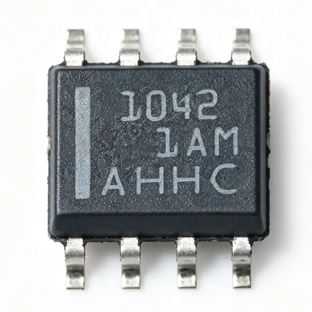
TCAN1042GVDRQ1 - Automotive CAN FD Transceiver | Texas Instruments
TCAN1042GVDRQ1 is an automotive fault-protected CAN transceiver from Texas Instruments, supporting CAN FD data rates up to 5 Mbps with I/O level shifting. It is housed in an 8-pin SOIC (D) package and operates across a temperature range of -55°C to 125°C. A CAN transceiver is a physical layer interface between a CAN controller and the CAN bus twisted-pair wiring. It converts the differential CAN bus signals (CANH/CANL) into single-ended logic levels for the controller, and vice versa. In automotive and industrial networks, the transceiver must handle harsh electrical environments, including voltage transients, ground offsets, and short-circuit conditions, all of which TCAN1042GVDRQ1 is designed to protect against. Key features include fault protection against bus short-circuits and high-voltage transients, I/O level shifting for interfacing with 3.3V or 5V controllers, flexible data-rate operation up to 5 Mbps, and low-power standby mode. The device meets the requirements of ISO 11898-2 for automotive CAN, providing robust communication with a 1/1 driver/receiver configuration and half-duplex operation. Technically, TCAN1042GVDRQ1 integrates a differential driver and receiver, providing differential transmit and receive capability. The I/O level shifting feature allows direct connection to microcontrollers with lower logic levels, eliminating the need for external level translators. Fault protection safeguards the device and bus against short circuits, thermal stress, and voltage surges, ensuring reliable communication in noisy environments. Typical applications include automotive body control modules, gateways, battery management systems, industrial automation, and medical devices where reliable CAN communication is required. The wide operating temperature range and AEC-Q100 qualification (implied by automotive designation) make it suitable for under-hood and harsh environment deployments. During design, ensure proper decoupling capacitors (100 nF and 10 uF) are placed close to the VCC pin to minimize noise, and use the appropriate bus termination resistors (120 ohms) at both ends of the bus. The SOIC-8 package allows compact PCB layouts, but thermal management should be considered for high-temperature environments.

TCAN1044DRQ1 - 8Mbps CAN FD Transceiver, 8-SOIC | Texas Instruments
The Texas Instruments TCAN1044DRQ1 is an automotive-qualified, high-speed Controller Area Network (CAN) transceiver meeting the physical-layer requirements of the ISO 11898-2:2016 standard. It supports both classical CAN and CAN FD (Flexible Data-Rate) networks at data rates up to 8 megabits per second (Mbps), and ships in an 8-pin SOIC (DRB) package with an operating temperature range of -40 C to +125 C. A CAN transceiver is a physical-layer interface IC that bridges a digital CAN protocol controller (typically embedded in a microcontroller) to a differential two-wire CAN bus. The transceiver translates the controller's single-ended TXD/RXD logic signals to the bus's dominant/recessive differential signaling required by ISO 11898-2, while providing bus-side ESD protection, common-mode range, and dominant-time-out fault protection. The TCAN1044-Q1 family sits in the CAN interface IC -> interface IC -> integrated circuit hierarchy and is a foundational building block for in-vehicle networks (IVN). Key features include 8 Mbps CAN FD data-rate support for next-generation vehicle networks, IEC 61000-4-2 ESD protection on bus pins, low-loop delay for propagation-tight networks, and a low-power standby mode with a remote-wake-up wake request via the bus (per the TCAN1044 family datasheet). The device operates from a single 4.5 V to 5.5 V VCC supply, draws typically 50 mA in normal mode, and integrates thermal shutdown plus bus-dominant time-out to prevent network lockup. The TCAN1044DRQ1 architecture uses a high-speed differential driver and a wide-common-mode receiver that exceeds the -2 V to +7 V common-mode range required by ISO 11898-2:2016. Internal level shifting on TXD/RXD allows direct connection to 3.3 V or 5 V microcontrollers without external logic-level translators, and the integrated bus fault protection tolerates -58 V to +58 V transients common in automotive 12 V/24 V systems. Typical applications include automotive body and chassis CAN nodes (BCM, gateway modules), CAN FD powertrain networks, industrial CAN-bus field-bus nodes, and electric-vehicle battery management system (BMS) master/slave communication. The AEC-Q100 Grade 1 qualification makes it appropriate for under-hood and safety-critical vehicle ECUs. When designing with this part, observe the 60 ohm bus termination requirement of ISO 11898-2 and place a 100 nF VCC decoupling capacitor within 2 mm of the supply pin. Avoid routing the CANH/CANL differential pair over splits in reference planes, and use a 120 ohm characteristic-impedance cable/trace geometry. This page synthesizes distributor pricing, drop-in pin-compatible alternatives, and practical PCB design notes for the TCAN1044DRQ1 - information not consolidated in the manufacturer datasheet alone.

TCAN1051-Q1 - Automotive Fault-Protected CAN FD Transceiver | Texas Instruments
TCAN1051-Q1 from Texas Instruments is an automotive fault-protected CAN transceiver with flexible data-rate and sleep mode, meeting ISO 11898-2 (2016) High-Speed CAN physical layer standard. It comes in an 8-pin SOIC package, supporting data rates up to 2 Mbps in CAN FD networks; variants with the G suffix support up to 5 Mbps, while V-suffix versions add a secondary power supply input for I/O voltage. A CAN transceiver is the physical-layer interface between a CAN protocol controller (MCU) and the two-wire differential CAN bus. In the automotive hierarchy, the CAN bus connects ECUs such as engine control, body control, and infotainment modules. The transceiver converts TXD/RXD logic signals from the MCU into differential CANH/CANL signals on the bus and provides bus fault protection. Key features include high on-chip IEC ESD protection, silent mode for reduced power consumption, and AEC-Q100 automotive qualification. The device is designed for harsh automotive environments, with fault protection that withstands bus transients. The flexible data-rate option enables CAN FD networks up to 5 Mbps, making it suitable for modern vehicle architectures that require higher bandwidth. The TCAN1051 family uses a robust physical-layer design with protection diodes and a dominant time-out function, ensuring reliability under bus shorts and high-voltage transients. The device supports both 5 V and (in V variants) 3.3 V I/O reference voltage, allowing direct interface with low-voltage microcontrollers. Typical applications include automotive body control modules, battery management systems, powertrain control, and industrial automation networks. The TCAN1051-Q1 is also widely used in diagnostics (OBD-II) and infotainment systems. Design consideration: ensure proper termination (120 ohm) and place TVS diodes and bus filtering capacitors close to the on-board connectors to prevent transient events from propagating into the PCB.

TCAN1051DRBRQ1 - Automotive CAN FD Transceiver | TI
The Texas Instruments TCAN1051DRBRQ1 is an automotive fault-protected CAN transceiver with CAN FD flexible data-rate support up to 2 Mbps, integrated sleep mode, and a 5 V supply, housed in an 8-pin VSON (DRB) 3x3 mm package rated from -55C to +125C. A CAN (Controller Area Network) transceiver is the physical-layer interface IC that converts the logic-level TXD and RXD signals of a CAN controller into the differential CANH and CANL bus signals defined by ISO 11898. Within the vehicle networking hierarchy, the transceiver sits between the MCU/CAN controller and the twisted-pair bus, providing dominant/recessive signaling, bus fault protection, and low-power standby or sleep behavior for networked electronic control units. Key features include automotive AEC-Q100 qualification, fault protection on the CAN bus pins (protection against faults to battery, ground, and overvoltage per the TI TCAN1051-Q1 product page), CAN FD flexible data-rate support up to 2 Mbps, and a sleep mode that reduces quiescent current for always-on vehicle networks. The -55C to +125C operating range supports under-hood and chassis deployments. The device implements a half-duplex differential physical layer with integrated receiver and driver stages. Internal protection circuitry clamps bus-pin transients and survives DC fault conditions on CANH and CANL, reducing the need for extensive external TVS components in harsh 12 V and 24 V vehicle power environments. Typical applications include body control modules, gateways, ADAS sensor clusters, battery management systems, and industrial CAN networks requiring robust fault tolerance and low standby power. Design consideration: confirm the sleep-mode wake behavior and bus biasing scheme against the TI datasheet, and verify that the 3x3 mm VSON thermal pad is well soldered to ground for transient robustness. This page synthesizes verified distributor listings, drop-in same-family alternatives, and design guidance not consolidated in the manufacturer datasheet.

TCAN1145DRQ1 - Automotive CAN FD Transceiver | Texas Instruments
The Texas Instruments TCAN1145DRQ1 is an automotive CAN FD transceiver with selective wake and SPI-configurable operation, supporting data rates up to 5 Mbps and processor I/O voltages from 1.8 V to 5 V in a 14-pin SOIC package. It is designed for high-speed CAN networks that need enhanced data rates, reduced-node sleep operation, and controlled low-power wake behavior. A CAN transceiver is the physical-layer interface between a host processor and a Controller Area Network bus. The TCAN1145-Q1 family supports enhanced high-speed CAN FD and high-speed CAN operation, while its selective-wake function uses wake-up frame identification to reduce the number of active network nodes. Its SPI interface provides access to device configuration and status functions, allowing a microcontroller to manage transceiver behavior without relying on undisclosed control assumptions. The principal verified feature set includes support for CAN FD data rates up to 5 Mbps, nominal processor I/O operation from 1.8 V to 5 V, and selective wake for partial networking. The TCAN1145DRQ1 ordering variant is identified by DigiKey as a 1/1 half-CANbus transceiver in a 14-SOIC package. The TI product description also associates the device with automotive CAN FD applications and ISO 11898-2:2016-compatible selective-wake functionality. The device is intended for vehicle body, comfort, infotainment, gateway, and distributed control networks where sleeping nodes must be awakened selectively. Compared with a conventional always-on CAN transceiver, the selective-wake architecture can reduce activity in a partial network and preserve energy when only selected nodes communicate. The SPI interface also supports firmware-controlled configuration, which is useful when a system needs programmable bus-management behavior. Designers should confirm the complete electrical limits, pin functions, transceiver modes, ESD behavior, loopback behavior, and timing values from the manufacturer datasheet before layout release. CAN bus routing requires controlled differential impedance, appropriate termination, common-mode protection according to the vehicle design, and careful separation from noisy high-current paths. The transceiver should be placed near the connector and bus protection network, while SPI and ground returns should be routed away from the CANH and CANL conductors. TCAN1145DRQ1 is best suited to new automotive electronic systems that specifically need CAN FD, selective wake, SPI access, and a 1.8 V to 5 V processor interface. The TCAN1042HGDR comparison reference is useful for evaluating a different TI CAN transceiver, but it should not be treated as a drop-in replacement without confirming its pinout and electrical requirements. This page combines manufacturer information, distributor package identification, cross-reference context, and design guidance for engineering evaluation.
TCAN1472-Q1 - Automotive CAN SIC Transceiver, 8Mbps, 8-SOIC | TI
The Texas Instruments TCAN1472-Q1 is an automotive-grade, fault-protected CAN FD transceiver with Signal Improvement Capability (SIC) that supports classical CAN and CAN FD up to 8 Mbps, available in an 8-pin SOIC (D) package with industry-standard pin-out. It is qualified to AEC-Q100, listed as Functional Safety-Capable, and is designed to meet the physical-layer requirements of ISO 11898-2:2024 Annex A (CAN SIC). A CAN (Controller Area Network) transceiver is the physical-layer interface between a CAN protocol controller (typically an MCU or ASIC) and the differential CAN bus wiring. It converts the controller's TX/RX logic-level signals to the bus's dominant/recessive differential voltages and adds bus-side protection, fault detection, and EMC filtering. SIC is an optional extension layer that actively reshapes the bus waveform to reduce ringing on long stubs and high-speed topologies, allowing faster bit rates (up to 8 Mbps with CAN FD) on networks that previously had to slow down for signal integrity reasons. Key features of the TCAN1472-Q1 include: support for classical CAN and CAN FD up to 8 Mbps with active SIC; ±58 V (typ.) fault-protected CAN bus pins; IEC 61000-4-2 ESD rating of ±8 kV contact / ±15 kV air on bus pins; low-current standby mode with remote wake-up via bus; and an operating voltage range of 4.5 V to 28 V (load-dump tolerant up to 40 V). 'V'-suffix variants (e.g. TCAN1472VDRQ1, TCAN1472VDFFRQ1) include a VIO logic-level supply pin so the device can interface directly with 1.8 V / 2.5 V / 3.3 V MCUs without external level shifters. The device integrates a 3.3 V / 5 V tolerant reference output, thermal shutdown, driver-dominant time-out, and under-voltage lockout on both VCC and VIO. Its bus-side hardware meets ISO 11898-2:2024 Annex A (SIC), ISO 11898-2:2016, and SAE J2284, making it drop-in compatible with existing 8-pin CAN FD footprints such as TCAN1042-Q1 and TCAN1044A-Q1 while adding the SIC waveform improvement stage. Typical applications include automotive body and chassis ECUs (BCM, gateway, HVAC, lighting), ADAS sensor fusion ECUs, xEV battery-management and powertrain controllers, industrial CAN networks with long stub lengths, and any automotive CAN FD node that needs to coexist with classical CAN on the same bus. The wide supply range also makes the part well suited for 12 V and 24 V truck and off-road CAN bus systems. When designing with the TCAN1472-Q1, place a 100 nF decoupling capacitor as close as possible to VCC and (on V-suffix parts) VIO, and a 4.7 µF or larger bulk capacitor on the bus-side CAN supply. On long-stub networks, leave SIC enabled to suppress reflections; on point-to-point links SIC can be turned off for the lowest loop delay. Always verify that the chosen package thermal pad layout matches the 8-pin SOIC land pattern. This page synthesises TI datasheet parameters, distributor pricing tiers, and drop-in alternatives in the same 8-SOIC footprint - information not all collected on a single manufacturer page.
TCAN330D - 3.3V 1Mbps CAN Transceiver | Texas Instruments
Texas Instruments TCAN330D is a 3.3-V, one-half CAN bus transceiver with a maximum specified data rate of 1 Mbps, ISO 11898 high-speed CAN physical-layer compatibility, and an 8-pin SOIC package. It is designed to connect a 3.3-V CAN controller to a physical CAN bus in industrial, automotive, and embedded systems. The device also provides ultra-low-power Shutdown and Standby modes for battery-powered equipment. A CAN transceiver is the physical-layer interface between a digital CAN controller and the differential CANH and CANL bus conductors. Unlike a general-purpose differential line driver, a CAN transceiver combines transmit, receive, bus-fault, and low-power functions in one device. The TCAN330 belongs to the TCAN33x family of 3.3-V CAN transceivers and is positioned for systems using ISO 11898 high-speed CAN. Verified device features include one-half CAN transceiver operation, data rates up to 1 Mbps, 3.3-V operation, an 8-SOIC package, and Shutdown and Standby operating states. The SOIC package supports conventional surface-mount assembly, while the low-power modes are useful when a portable or battery-operated controller must disconnect from the bus without losing its local supply. Texas Instruments states that this family is available in standard 8-pin SOIC packages for drop-in compatibility. The TCAN330D physically separates the controller-side TXD and RXD signals from the bus-side CANH and CANL interface. Designers must still provide correct controller logic levels, bus termination, decoupling, and protection appropriate to the vehicle or industrial environment. The provided data does not establish every absolute maximum rating, transceiver delay, output-level value, or bus-fault threshold, so those specifications should be confirmed in the manufacturer datasheet before release. Typical uses include industrial automation controllers, electric-vehicle subsystems, battery management gateways, motor-control equipment, diagnostic interfaces, and embedded CAN nodes. For a compact design, the logic interface is tied to a 3.3-V CAN controller, while the differential bus side connects to CANH and CANL through the application's termination and protection network. Layout and power integrity remain critical even in an eight-pin interface IC. Place required decoupling capacitors close to the supply pins, keep bus traces short and appropriately routed as a differential pair, and verify common-mode and fault-tolerance requirements against the complete system. Because no verified pricing, lifecycle, or complete pin-level table was supplied, those details remain marked for confirmation rather than inferred. This product page combines verified distributor and manufacturer information, CAN physical-layer context, practical design guidance, and explicit data gaps. The resulting TCAN330D reference is intended to accelerate component review while keeping engineering decisions traceable to the supplied sources.
TCAN330DR - 3.3V 1Mbps CAN Transceiver | Texas Instruments
The Texas Instruments TCAN330DR is a 3.3-V high-speed CAN physical-layer transceiver specified for data rates up to 1 Mbit/s in an 8-pin SOIC package. It supports low-power shutdown and standby operation, making the device suitable for industrial automation, building control, embedded systems, and battery-powered equipment. The TCAN330 family is compatible with the ISO 11898 high-speed CAN physical-layer standard. A CAN transceiver is the physical-layer interface between a CAN controller and the differential CAN bus. It converts logic-level TXD and RXD signals into bus-compatible differential signaling, while the receiver converts bus levels back into logic. Within the hierarchy of CAN interface ICs, the TCAN330 belongs to the high-speed CAN transceiver class and combines bus-driver, receiver, protection, and low-power control functions. Verified device features include a 3.3-V supply-oriented design, operation up to 1 Mbit/s, 1/1 transceiver configuration, an 8-pin SOIC package, and shutdown and standby modes. The manufacturer states that the TCAN33x family is compatible with ISO 11898. Its low-power modes are intended to reduce consumption when a system is inactive or operating in a reduced-function state. The TCAN330 is intended for systems that use a separate CAN controller and require a physical-layer transceiver. Its 3.3-V interface orientation makes it particularly useful with low-voltage controllers and embedded processors. The standard 8-pin SOIC package also provides a practical migration path from conventional through-hole or larger-outline CAN implementations when board area permits. Typical use cases include industrial control networks, factory equipment, building-automation controllers, robotics, motor-control systems, and embedded communications modules. In these applications, the transceiver converts between the host controller and the CANH/CANL bus pair while supporting system-level power management through its low-power control functions. When laying out a TCAN330DR board, route CANH and CANL as a tightly coupled differential pair with continuous return-path geometry, place termination only where appropriate for the network topology, and keep high-current or high-voltage switching nodes away from the bus traces. Confirm the external controller voltage levels, bus protection requirements, and standby or shutdown polarity before finalizing the PCB.
TCAN332D - 3.3V, 1Mbps CAN Transceiver | Texas Instruments
The Texas Instruments TCAN332D is a 3.3 V single-supply CAN transceiver with a maximum signaling rate of 1 Mbps, one CAN channel, and an 8-pin SOIC package. It provides the physical-layer interface between a CAN controller and the differential CAN bus, supporting ISO 11898-2 high-speed CAN and CAN FD operation. The device is supplied from 3 V to 3.63 V and operates across the -40°C to +125°C temperature range. A CAN transceiver is a physical-layer interface IC that converts logic-level TXD and RXD signals into the dominant and recessive voltage levels used on a CAN bus. It also receives the bus differential voltage and returns a compatible controller signal. The TCAN332D belongs to the TCAN33x family of 3.3 V CAN transceivers with CAN FD support. Key features include 3.3 V single-supply operation, ISO 11898-2 compatibility, a 1 Mbps maximum signaling rate, and receiver common-mode input capability from -2 V to 7 V. The family also includes devices with data rates up to 5 Mbps, although the verified TCAN332D ordering information identifies the TCAN332D as a 1 Mbps CAN device. Ultra-low-power shutdown and standby functionality makes the family suitable for battery-powered equipment. The TCAN332D uses separate transmit, receive, ground, and CAN bus connections. Its differential bus architecture supports noisy automotive and industrial environments, while the transceiver-level logic interface connects directly to a CAN controller. Engineers should verify loopback, bus termination, fault behavior, and timing against the manufacturer datasheet before deploying a new network. Typical applications include automotive electronic control units, industrial automation equipment, robotics, building controls, battery-powered sensors, and CAN FD gateways. The 8-pin SOIC package supports conventional PCB assembly and is identified by Texas Instruments as available for drop-in-compatible CAN family implementations. Design attention should focus on decoupling, termination, common-mode range, ground return, and protection from transients. A 120-ohm termination is normally placed at each end of a properly terminated CAN bus, but the final network topology and protection strategy must match the system requirements. This page consolidates verified manufacturer and distributor information, same-package alternatives, application guidance, and design notes for engineers evaluating the TCAN332D.
TCAN334D - 3.3V CAN FD Transceiver | Texas Instruments | Industrial
The Texas Instruments TCAN334D is a 3.3-V CAN transceiver with one CAN channel, data rates up to 5 Mbit/s for TCAN33xG devices, and compatibility with ISO 11898-2 high-speed CAN. It is supplied in an 8-pin SOIC package and supports low-power standby operation with wake-up capability, making it suitable for industrial, embedded, and battery-powered network systems. The device operates from a single 3.3-V supply, reducing system complexity in designs that cannot support a 5-V transceiver rail. A CAN transceiver is the physical-layer interface between a CAN controller and the differential CAN bus. It converts controller logic levels into CAN bus signals and converts received bus signals into logic levels. The TCAN334D belongs to the TCAN33x family of 3.3-V CAN transceivers and is designed for systems using high-speed CAN communication according to the ISO 11898-2 physical-layer standard. The principal feature of the TCAN334D is its low-power behavior. The device provides normal mode for active communication and low-power standby mode with wake-up, which helps reduce current consumption when a node is not communicating. Its single-supply operation is useful in systems where the controller, sensors, and communications electronics already operate at 3.3 V. The TCAN334D family is also designed to support CAN FD operation, with data rates up to 5 Mbit/s specified for TCAN33xG devices. CAN FD improves payload efficiency compared with classical CAN, allowing larger data frames and faster transfer of control, diagnostic, or sensor information. Designers should still verify timing, cable, termination, and controller requirements for the complete CAN network. Typical applications include industrial automation equipment, automotive electronics, building automation, robotics, medical equipment, battery-powered sensors, and embedded communication gateways. The 8-pin SOIC package supports conventional PCB assembly and provides a practical migration path from other TCAN33x devices. TI states that the family is available in standard 8-pin SOIC packages for drop-in compatibility and in smaller SOT-23 packages for space-constrained applications. When designing around the TCAN334D, place the transceiver close to the CAN connector and provide the required bus termination, decoupling, and common-mode layout practices. Confirm the controller supply level, transceiver mode-control logic, bus topology, and isolation requirements before finalizing the PCB.

TCAN334DCNR - 3.3V CAN FD Transceiver, SOT-23-8 | Texas Instruments
The Texas Instruments TCAN334DCNR is a 3.3-V Controller Area Network (CAN) transceiver supporting CAN FD (Flexible Data Rate) up to 1 Mbps, housed in an 8-pin SOT-23 (DCN) package. Designed for ISO 11898-1 High-Speed CAN physical layer compliance, it integrates a 1/1 (one transmit, one receive) transceiver half between a CAN protocol controller and the physical bus, with low power Shutdown and Standby modes for battery-powered applications. A CAN transceiver is a physical-layer interface IC that converts the differential digital signals of a CAN protocol controller into the robust, fault-tolerant differential signaling required on the automotive or industrial CAN bus. Within the broader hierarchy, a CAN transceiver sits below the CAN controller (typically integrated in an MCU) and above the physical twisted-pair bus; it belongs to the Interface ICs > Networking transceivers category and is essential for in-vehicle networking (CAN, CAN FD), industrial automation (CANopen, DeviceNet), and any distributed control system requiring reliable multi-node communication. Key features include 3.3-V single-supply operation compatible with 3.3-V MCUs (no level shifter required), ultra-low current consumption in Shutdown/Standby modes, integrated bus dominant time-out protection, thermal shutdown, and an internal slope-control / driver output that meets the ISO 11898-2 (High-Speed CAN) requirements. Logic-side inputs are TTL-compatible and tolerate 5-V MCU rails. The TCAN334DCNR uses TI's BiCMOS process, allowing the high-voltage bus side (up to +-18-V fault on CANH/CANL) to coexist with the low-voltage 3.3-V digital core. Loop-delay symmetry is optimized for CAN FD frames with payload bit rates beyond 1 Mbps on the data phase, ensuring robust arbitration-to-data transitions. Typical applications include automotive body electronics (door modules, HVAC, seat controllers), industrial sensor networks, building automation, battery management (BMS) slave-node communication, and any 3.3-V MCU system requiring a compact CAN physical interface. When designing with this device, ensure the CAN bus termination (typically 120 ohms at each bus end) is correct, and route the CANH/CANL traces as a 100-ohm differential pair on the PCB. The 8-pin SOT-23 footprint gives strong thermal coupling for a small package, allowing sustained high-bus-traffic operation without exceeding junction ratings. This page synthesizes distributor pricing, drop-in alternatives, and practical design notes not found in the manufacturer datasheet alone, supporting faster design decisions for embedded engineers.
TCAN337D - 3.3 V, 1 Mbps CAN FD Transceiver | Texas Instruments
The Texas Instruments TCAN337D is a 3.3 V CAN FD transceiver with one CAN transmitter and one CAN receiver, a maximum specified data rate of 1 Mbps, and an 8-pin SOIC package. It is designed for 3.0 V to 3.6 V supply operation and supports operation from -40°C to 125°C. The device provides a half-duplex physical-layer interface between a CAN controller and a high-speed CAN bus. A CAN transceiver is the physical-layer interface within a Controller Area Network. A CAN controller generates and interprets digital frames, while the transceiver converts that logic-level information into differential bus signals and receives bus states back into logic-compatible signals. The TCAN33x family is compatible with the ISO 11898 High-Speed CAN Physical Layer standard, as stated on the Texas Instruments product page. The TCAN337D combines a 3.3 V operating range with a stated data rate of up to 1 Mbps and CAN FD support. Its supply current is listed as 180 mA in the supplied cross-reference data, while the receiver hysteresis is 120 mV. The 8-SOIC package is identified by DigiKey as a surface-mount package, and the family documentation states that the standard 8-pin SOIC packages support drop-in compatibility. Typical bus applications include industrial automation equipment, embedded controllers, vehicle electronics, battery-powered instruments, and other 3.3 V systems that communicate over a high-speed CAN network. Because CAN is a multi-node differential bus, transceiver placement, termination, grounding, and controller compatibility remain important system-level considerations. For a new PCB, place the transceiver close to the bus connector and CAN controller, provide a continuous ground reference, route the differential bus as a coupled pair, and install the required 120-ohm termination only at appropriate bus endpoints. Existing designs should verify voltage levels, pin mapping, transceiver mode, and timing before upgrading. This page combines verified manufacturer and distributor information, explicit data gaps, and engineering guidance for selecting and implementing the TCAN337D. It does not infer undocumented electrical limits, pricing, or cross-brand replacements.
TCAN337DR - 3.3V CAN FD Transceiver | Texas Instruments
The Texas Instruments TCAN337DR is a 3.3 V single-channel CAN transceiver with CAN FD support, designed for 3 V to 3.6 V operation and data rates up to 1 Mbps in an 8-pin SOIC package. It provides a compact physical-layer interface between a CAN controller and the differential CAN bus, while supporting ISO 11898-2 high-speed CAN communication. A CAN transceiver, also called a CAN bus interface IC, converts logic-level TXD and RXD signals into the differential CAN bus voltage and back again. In the system hierarchy, it belongs to interface ICs and specifically to the CAN physical-layer family. The TCAN337DR supports normal mode, silent mode, low-power shutdown, and standby operation, making it useful for both continuously connected and battery-powered equipment. Key verified features include 3.3 V single-supply operation, 3 V to 3.6 V supply range, up to 1 Mbps signaling rate, CAN FD compatibility, ISO 11898-2 compatibility, and an 8-pin SOIC package. The listed operating temperature is -40°C to 125°C, making the device suitable for industrial and automotive-temperature environments when the complete system satisfies its qualification requirements. The TCAN337 family includes a standard 8-pin SOIC option intended for drop-in compatibility, while SOT-23 options address space-constrained designs. TCAN337G variants extend the signaling rate to 5 Mbps, whereas the TCAN337DR is identified as a 1 Mbps device. This distinction is important when selecting a replacement or comparing newer CAN FD hardware. Typical applications include industrial automation equipment, automotive and transportation electronics, robotics, building controls, and embedded CAN gateways. The 3.3 V supply operation is especially useful with low-voltage processors, while the transceiver isolates the logical interface from the physical bus wiring. Designers should provide correct bus termination, a suitable common-mode network, and compliant transceiver decoupling. The SOIC footprint simplifies conventional leaded-board assembly, but exposed-pad-free packages may limit heat dissipation compared with an exposed-pad option. Verify the exact logic levels, bus fault limits, standby behavior, and CAN FD timing before substituting another device.
TCAN3403-Q1 - 3.3V Automotive CAN FD Transceiver | TI
The Texas Instruments TCAN3403-Q1 is an automotive-grade 3.3 V Controller Area Network (CAN) Flexible-Data-Rate (FD) transceiver with flexible I/O and standby mode, available in 8-pin SOIC (D) and 8-pin SON (DRB) packages. It supports data rates up to 5 Mbps (CAN FD) and is compliant with ISO 11898-2:2016 physical-layer requirements, including ±58 V bus fault protection for 12 V and 24 V battery systems. Internal logic-level translation through the VIO pin (1.7 V to 5.5 V) allows direct interface to 1.8 V, 2.5 V, or 3.3 V MCUs without an external level shifter. A CAN transceiver (also called a CAN physical-layer or CAN PHY) is the analog interface IC that sits between a digital CAN protocol controller (typically inside an MCU) and the differential CANH/CANL bus wires. It converts the controller's transmit (TXD) digital stream into a balanced differential signal on the bus and vice versa, while providing dominant/common-mode biasing, ESD protection, bus-fault survival, and optional low-power modes. CAN FD extends classic CAN by increasing payload size (64 bytes) and bit rate (up to 5 Mbps in the data phase), enabling higher bandwidth for automotive body, chassis, and powertrain networks; the TCAN3403-Q1 operates seamlessly on mixed classic CAN and CAN FD networks. Key features of the TCAN3403-Q1 include AEC-Q100 Grade 1 qualification for automotive use, ±58 V bus standoff (versus typical ±40 V parts), low-loop delay for FD arbitration, thermal-shutdown protection, and a standby mode with remote-wake request via the bus (per ISO 11898-2:2016). The 3.3 V single-supply operation eliminates the 5 V LDO that older 5 V transceivers required, reducing BOM cost and PCB area by roughly 10-30 mm². The device uses a symmetric differential driver architecture with controlled edge rates to minimize EMI and reflections on unterminated stubs. Integrated protection includes undervoltage lockout on both VCC and VIO, TXD dominant-timeout to prevent bus lockup, hot-plug support, and ±25 kV HBM / ±12 kV IEC 61000-4-2 contact discharge ESD on the bus pins. Typical automotive applications include body-control modules (BCM), gateway ECUs, infotainment domain controllers, ADAS sensor ECUs, and industrial CAN-FD nodes needing automotive-grade qualification. The wide bus-fault range also makes it suitable for 24 V truck and off-road machinery CAN buses where legacy 5 V parts would fail. Designers should add a 100 nF decoupling cap on VCC and VIO placed within 2 mm of the pins, and a common-mode choke plus split termination (60 Ω + 60 Ω with 4.7 nF to ground) on the bus side for IEC 61000-4-2 ESD compliance and best EMI performance. The STB pin enables standby mode (~15 µA ICC), so connect it to a GPIO for software-controlled sleep. This page synthesizes distributor pricing, drop-in alternatives, and practical design notes not found in the manufacturer datasheet.
TCAN3404-Q1 - Automotive 3.3V CAN FD Transceiver | Texas Instruments
The Texas Instruments TCAN3404-Q1 is an automotive-qualified 3.3V CAN flexible-data-rate (CAN FD) transceiver that supports data rates up to 8 Mbps and is housed in an 8-pin TSOT-23 (DDF) package. The device integrates ±58V bus fault protection and is compliant with the ISO 11898-2:2016 high-speed CAN physical layer specification. It is AEC-Q100 qualified for automotive applications and supports both low-power standby mode (controlled via the STB pin) and an ultra-low-power shutdown mode (controlled via the SHDN pin). A CAN FD transceiver, also called a CAN physical-layer (PHY) device, is the interface between a digital CAN controller (or microcontroller with integrated CAN MAC) and the differential CAN bus wires. It converts the controller's transmit (TXD) and receive (RXD) single-ended logic signals into differential bus voltages (CANH, CANL), and provides bus arbitration, fault protection, and ESD handling for the harsh automotive electrical environment. The TCAN3404-Q1 belongs to the broader category hierarchy of: CAN transceiver → CAN interface IC → serial interface IC → wired connectivity IC → interface & connectivity semiconductor. The 3.3V (rather than 5V) supply rail reduces power loss in modern automotive MCU domains. Key features include ±58V bus fault tolerance (industry-leading for the 8-pin TSOT-23 form factor), ±25V common-mode range on CANH/CANL, 8 kV HBM ESD protection on bus pins, low-loop delay to support 8 Mbps CAN FD frames, and ultra-low-power shutdown current. Internal pull-down resistors on STB and SHDN default the device to safe operating states if pins are left floating. The TSOT-23-8 package measures 2.9 mm × 1.6 mm and is well suited for space-constrained body electronics and zonal ECU modules. Architecturally, the TCAN3404-Q1 uses a single 3.3V supply rail, eliminating the need for an external charge pump or 5V regulator that legacy 5V CAN transceivers sometimes require. The transmitter and receiver share a common-mode reference and slope-control circuitry, allowing fast bit transitions while minimizing EMI on unshielded twisted-pair automotive harnesses. The device is designed for robust coexistence on mixed 3.3V/5V CAN networks, with a recessive bias that minimizes error frames during arbitration. Typical applications include automotive body control modules, gateway ECUs, ADAS sensor CAN-FD links, battery management system (BMS) communication buses, and infotainment CAN backbones. It is also used in industrial CAN-FD nodes and heavy-truck J1939 networks where ±58V load-dump survival is required. The shutdown mode is particularly useful in battery-powered systems that need to enter sleep states with the bus still biased. Designers should pair the TCAN3404-Q1 with a 3.3V CAN-capable MCU (such as TI's TMS570 or C2000 families) and provide a common-mode choke plus split termination on the bus to maximize radiated-emissions margin. Care must be taken not to leave SHDN floating in mission-critical designs; tying it to logic high enables ultra-low-power mode when the ECU shuts down. This page aggregates distributor stock, verified drop-in replacement MPNs (including the closely-related TCAN3403-Q1 and TCAN3413-Q1), and engineering design notes that supplement the manufacturer datasheet with PCB-layout, ESD, and mixed-voltage coexistence guidance.
TCAN3413 - 3.3V CAN FD Transceiver, ±58V Bus Fault, SOIC-8 | TI
The Texas Instruments TCAN3413 is a 3.3-V Controller Area Network Flexible Data-rate (CAN FD) transceiver in an 8-pin SOIC (D) package with ±58-V bus fault protection, ISO 11898-2:2016 compliance, and certified EMC operation up to 5 Mbps. It includes internal logic-level translation via the VIO pin that allows the I/O side to interface directly to 1.8-V, 2.5-V, or 3.3-V logic, eliminating the need for an external level shifter on multi-voltage MCUs. The device supports a low-power standby mode with wake-up over CAN that conforms to the ISO 11898-2:2016 wake-up pattern (WUP), making it well suited to automotive body and industrial remote-IO applications that must stay quiescent until bus activity resumes. A CAN bus is a differential, multi-drop vehicle and industrial field bus originally specified by Bosch and standardized by ISO 11898; CAN FD extends classical CAN from 1 Mbps to 5 Mbps and increases payload from 8 bytes to 64 bytes, while the physical-layer chip (the transceiver) adapts digital logic to the differential bus and protects downstream devices from the harsh bus-side environment. The TCAN3413 belongs to the TI CAN physical-layer IC family, which sits between the protocol controller (in the MCU) and the differential bus lines, and is widely deployed alongside TCAN3414 in the same product family. The device is a direct successor to legacy 3.3-V CAN transceivers and provides higher bus-fault tolerance, robust ESD protection on the bus pins, and more flexible power-saving options. Typical use cases include automotive body electronics, industrial control CAN nodes, building-automation sensors, and telecom base-station housekeeping buses. When designing with this part, ensure the VIO supply matches the MCU logic level and that bus termination follows ISO 11898-2:2016 guidance, as improper stub length and missing 120 ohm terminations are the leading cause of bus error frames. This page synthesizes distributor pricing, drop-in alternatives from the same TI CAN family, and practical design notes not found in the manufacturer datasheet.
TCAN3414 - 3.3V CAN FD Transceiver, 5Mbps, ±58V Bus Fault | Texas Instruments
The Texas Instruments TCAN3414 is a 3.3-V Controller Area Network Flexible Data Rate (CAN FD) transceiver with standby mode, supporting data rates up to 5 Mbps and providing ±58-V bus fault protection. Housed in 8-pin SOIC (D) and 8-pin SON (DRB) packages, it is designed for industrial, automotive, and building-automation networks that need robust communication in electrically harsh environments. A CAN transceiver is the physical-layer interface between a CAN protocol controller (typically a microcontroller's CAN module or an external CAN controller) and the differential CAN bus. It converts the controller's digital transmit/receive signals into the ISO 11898-2:2016 compliant differential bus levels, while providing ESD protection, common-mode rejection, and bus fault tolerance. Within the broader hierarchy, a CAN transceiver sits below the CAN controller and above the physical wiring harness, and is itself a type of line driver / interface IC in the Interface > Interface ICs category. Key features include certified electromagnetic compatibility (EMC) for classical CAN and CAN FD up to 5 Mbps, ±58-V bus fault protection on the CANH/CANL pins, ±30-V common-mode range, and ±8-kV HBM ESD protection per IEC 61000-4-2 contact discharge on bus pins. The 1.7-V to 3.6-V IO range allows direct interfacing with 1.8-V, 2.5-V, 3.3-V, and 5-V microcontrollers without level shifters. A standby mode (via the STB pin) reduces quiescent current for low-power system sleep states. From an architecture standpoint, the TCAN3414 integrates a high-speed differential line driver, a differential comparator receiver, internal slope control for reduced EMI, and thermal-shutdown protection. The driver exhibits typical loop delay under 200 ns, allowing robust CAN FD performance at 2 Mbps and 5 Mbps. The internal protection circuitry clamps inductive transients on the bus, and the device meets the GIFT/ICT compliant IEC 62228-3 and IEC 61000-4-2 standards for ESD on bus pins. This combination makes the TCAN3414 a robust drop-in upgrade for older 3.3-V CAN transceivers such as the SN65HVD233/234/TCAN332 families. Typical applications include industrial CAN nodes (PLC modules, motor drives, sensors), building-automation HVAC controllers, battery-management system (BMS) communication in 48-V mild-hybrid and energy-storage systems, automotive body and infotainment ECUs, and any embedded design that needs certified EMC and high bus-fault tolerance on a 3.3-V rail. The ±58-V bus fault protection eliminates the need for external TVS diodes in most 12-V and 24-V industrial systems, simplifying BOM and reducing PCB area. When designing with this device, place the VIO/VCC decoupling capacitors as close as possible to the device pins and use a 100-nF X7R ceramic plus a 1-µF bulk capacitor. Ensure the CAN bus is terminated with 120-Ω resistors at each end of the bus (per ISO 11898-2), and keep the CANH/CANL traces as a tightly coupled differential pair to minimize EMI emissions. This page synthesizes distributor pricing, drop-in alternatives, application guidance, and design notes that go beyond what the manufacturer datasheet alone provides. XAIPART cross-references verified stock from authorized distributors and pairs it with parametric comparison tables to help engineers select the correct 3.3-V CAN FD transceiver for industrial and automotive designs.

TCAN4572-Q1 - Automotive CAN FD Controller + SIC Transceiver | TI
The Texas Instruments TCAN4572-Q1 is an automotive-grade CAN FD controller with an integrated CAN Signal Improvement Capable (SIC) transceiver, housed in a VQFN-24 package. It combines an ISO 11898-1:2015 compliant CAN FD protocol controller with an ISO 11898-2:2016 compliant physical layer transceiver, supporting data rates up to 8 Mbps with SIC enabled for improved signal integrity on long or star-topology bus networks. A CAN FD (Controller Area Network Flexible Data-Rate) controller with integrated transceiver is a system-on-chip that combines a CAN protocol engine and a physical layer transceiver in one device. The protocol controller manages message framing, arbitration, and error handling per the ISO 11898-1 standard, while the transceiver converts digital logic levels to the differential CANH/CANL bus signals per ISO 11898-2. By integrating both blocks, the TCAN4572-Q1 reduces PCB area, BOM count, and host MCU CAN peripheral requirements, placing it within the broader hierarchy of automotive interface IC > CAN interface > CAN FD transceiver/controller > in-vehicle networking IC. Key features include support for classic CAN and CAN FD frames, an SPI interface to the host microcontroller, AEC-Q100 qualification for automotive applications, and SIC (Signal Improvement Capability) for cleaner signal edges on complex topologies. The device operates over a wide supply range suitable for 12V automotive battery rails and includes thermal shutdown, bus dominant time-out, and undervoltage protection. The architecture pairs a dedicated CAN FD controller core with a low-emission differential transceiver. By performing in-situ signal conditioning via SIC, the TCAN4572-Q1 allows designers to deploy CAN FD networks across unshielded cable, mixed topologies, or nodes with significant stub lengths without compromising the bit-time budget. Typical applications include automotive body and chassis ECUs, ADAS sensor networks, battery management system (BMS) communication in electric vehicles, industrial CAN FD gateways, and CAN FD Light systems. The integrated MCU interface simplifies bring-up across zonal architectures where the host processor may lack an on-chip CAN FD peripheral. Designers must evaluate bus topology termination, stub length, and SIC enable/disable timing relative to network jitter budgets. The SPI clock and chip-select routing should be kept short to avoid protocol-controller timing violations during bus error interrupts. This page synthesizes distributor availability, drop-in alternative candidates, and practical design guidance drawn from the Texas Instruments TCAN4572-Q1 datasheet in a single product brief not found on the manufacturer page or distributor listings alone.
TCAN6062-Q1 - CAN XL Transceiver, AEC-Q100, SOIC-8 | TI
The Texas Instruments TCAN6062-Q1 is an automotive-grade, high-speed Controller Area Network (CAN) transceiver that meets the physical layer requirements of the ISO 11898-2:2024 Annex A (CAN XL) specification, housed in an 8-pin SOIC (D) package. Key parameters include CAN XL data-rate support up to 20 Mbps, integrated Signal Improvement Capability (SIC) mode, and PWM decoding on the TXD pin for FAST TX/FAST RX operation. A CAN transceiver is a physical-layer interface IC that converts the differential CAN bus signals (CANH, CANL) into the single-ended TXD/RXD logic levels required by a host microcontroller or CAN controller. It sits in the hierarchy bus transceiver -> bus interface IC -> interface IC -> semiconductor, providing galvanic isolation, level shifting, bus dominant/recessive arbitration, and EMC/ESD protection for the in-vehicle network. Modern CAN XL extends classical CAN and CAN FD by adding a higher data-rate payload channel while preserving backward compatibility with ISO 11898-2. Key features include an integrated standby mode for low-power sleep current, ±8 kV IEC 61000-4-2 ESD protection on the bus pins, ±58 V bus fault protection, and AEC-Q100 Grade 1 qualification (–40 °C to +125 °C ambient). The TCAN6062-Q1 also supports PWM-decoded signaling on TXD, enabling the SIC mode to actively reduce signal ringing during dominant-to-recessive transitions, which is critical for reliable multi-drop CAN XL networks at high data rates. The device architecture pairs a high-speed differential driver/receiver pair with an internal logic core that monitors TXD and decodes PWM-coded commands to switch between normal, FAST TX, FAST RX, SIC, and standby states. Compared with legacy CAN FD transceivers (e.g. TCAN1044A-Q1), the TCAN6062-Q1 adds CAN XL PHY support and the signal-conditioning features required for ISO 11898-2:2024 Annex A compliance, while remaining pin-compatible to 8-pin SOIC footprints used by prior TCAN families. Typical applications include automotive CAN XL backbone and zone-architecture networks, ADAS sensor ECUs (radar, lidar, camera), powertrain and chassis CAN nodes, body-domain controllers, and industrial CAN networks migrating from CAN FD to CAN XL. A key design consideration: ensure the bus termination (typically 120 Ω at each end of the CAN XL backbone, with SIC transceivers often allowing split termination) is sized according to the cable DC resistance and number of in-line stubs. STB pin logic levels must respect the wake/sleep timing in the datasheet to avoid bus contention on cold-start. This page synthesizes manufacturer specifications, distributor availability, AEC-Q100 compliance signals, and same-package cross-reference MPNs (TCAN1044A-Q1, TCAN1472-Q1) into a single engineering reference not duplicated on the TI datasheet alone.

TDA19989BET/C1,557 - 150MHz HDMI 1.4 TX | NXP Semiconductors
The NXP Semiconductors TDA19989BET/C1,557 is a 150 MHz pixel rate HDMI 1.4 transmitter video IC with 3 x 8-bit video inputs, HDCP 1.3 content protection, and CEC support, housed in a 64-pin TFBGA (4.5 x 4.5 mm) package. A video transmitter IC (also called an HDMI transmitter or video encoder) is an interface IC that converts a parallel digital video stream, such as ITU-R BT.656 or RGB data, into a serial TMDS (Transition Minimized Differential Signaling) signal compliant with HDMI or DVI standards. In the signal-chain hierarchy, it sits between a graphics source or video processor and the HDMI physical connector, performing serialization, encoding, and content-protection tasks required by the CEA-861B, HDMI 1.3a/1.4, and DVI 1.0 specifications. Key features include support for CEA-861B, DVI 1.0, HDMI v1.3a and HDMI 1.4 formats, HDCP 1.3 for encrypted content delivery, an I2C control interface, and ITU656 video input compatibility. The 150 MHz pixel rate supports video resolutions up to 1080p, while the 64-TFBGA footprint keeps board area to approximately 20.25 square millimeters for space-constrained designs. Architecturally, the TDA19989B family integrates TMDS serializers, an HDCP cipher engine, an audio return and CEC block, and flexible input multiplexing for three 8-bit video buses. The I2C register interface allows a host microcontroller to configure timing, audio, and protection parameters. The C/1,557 ordering suffix identifies the standard-rated commercial temperature grade in tape-and-reel packaging. Typical applications include set-top boxes, digital televisions and monitors, AV receivers, video projectors, and embedded systems that must output HDMI while processing ITU656 or RGB video internally. When designing with this device, provide a stable low-jitter TMDS reference clock and follow NXP layout guidance for 100-ohm differential impedance routing on the HDMI lanes; HDCP key handling also requires attention to firmware security practices. This page synthesizes distributor inventory data, drop-in alternative guidance, and practical design notes not found in the manufacturer datasheet alone.
TDA19989BET/C1551 - 150MHz HDMI 1.4 Transmitter | NXP
The NXP TDA19989BET/C1551 is a 150 MHz pixel rate HDMI 1.4 transmitter IC with HDCP 1.3 content protection and CEC support, housed in a 64-ball TFBGA (4.5 x 4.5 mm) package. It accepts parallel digital video (RGB/YCbCr, ITU656) and serializes it for HDMI or DVI output at pixel rates up to 150 MHz. An HDMI transmitter is a video interface IC that converts parallel or digital video bus data into the TMDS (Transition Minimized Differential Signaling) serial stream defined by the HDMI and DVI standards. Within the system hierarchy, it sits in the video signal chain between a graphics source (SoC, FPGA, or video processor) and the physical HDMI connector, and belongs to the broader class of interface ICs and video processing ICs. Key features include the 150 MHz pixel clock supporting 1080p60 video, compliance with CEA-861B, DVI 1.0, and HDMI v1.3a signaling with HDMI 1.4 capability, and integrated HDCP 1.3 cipher engine for protected content. An I2C host interface programs registers, controls the HDCP state machine, and reads EDID from the sink via DDC. CEC support enables consumer electronics control channel communication over the HDMI cable. Architecturally, the TDA19989 family combines input video formatting, TMDS serialization, audio embedding, infoframe generation, and HDCP encryption in a single low-power CMOS die. The 3 x 8-bit video input bus accepts RGB or YCbCr formats, while audio is accepted via I2S or S/PDIF-style inputs and multiplexed into the TMDS stream. Typical applications include set-top boxes, Blu-ray/DVD players, digital media adapters, automotive infotainment head units, and embedded boards with HDMI display outputs. Its compact 4.5 mm BGA suits space-constrained consumer and industrial designs. Designers should note that HDCP license agreements govern use of the cipher, and that the 64-TFBGA requires controlled-impedance TMDS routing on the PCB. Note the part is listed as obsolete by some sources, so verify lifecycle for new designs. This page synthesizes distributor pricing, same-family drop-in alternatives, and practical design notes not found in the manufacturer datasheet.

TDA51S-41HC - 5kVrms Isolator w/ DC-DC 150Mbps | MORNSUN
The MORNSUN TDA51S-41HC is a high-performance reinforced digital isolator with an integrated isolated DC-DC converter, providing 5000Vrms isolation, 150Mbps signal rate, and 150kV/us common-mode transient immunity in a 16-pin SOIC-16-300mil (wide-body) package. It operates from -40C to +125C, with a primary-side supply of 3.13V to 3.56V (3.3V nominal) and a secondary-side supply supporting up to 5.5V, and carries a UL1577-based 5000Vrms isolation rating. An isolated data transceiver with an integrated isolated power supply is a device that combines galvanic signal isolation and an on-chip (or on-module) isolated power source in one package. In the power-management hierarchy, it sits above standalone digital isolators, which require a separate isolated DC-DC converter or power module to energize the isolated side. By eliminating that external isolated supply, this device class delivers a complete, small-form-factor isolation solution with fewer components, lower BOM cost, and reduced layout risk. Key features of the TDA51S-41HC include the integrated isolated DC-DC converter, which removes the need for a separate isolated power supply; 150Mbps data rate for high-speed serial links; 150kV/us CMTI for immunity against fast switching transients typical of SiC and IGBT power stages; 5000Vrms reinforced isolation per UL1577; and a wide -40C to +125C industrial operating range. The device provides three forward-direction and one reverse-direction channel, with a fail-safe option: if the input signal is lost, the default output is low for devices with the H suffix, which matches the 41HC suffix in this MPN. The integrated power architecture uses on-chip transformer-based isolation for both signal and power transfer, keeping the total solution footprint small while maintaining reinforced-insulation creepage and clearance in the SOIC-16-300mil wide body. Typical applications include isolated RS-485/fieldbus nodes in industrial automation, isolated power and communication for IGBT/SiC gate-drive circuits, battery management systems, and PLC I/O modules. The combination of signal and power isolation is especially valuable where board space or single-supply constraints make a discrete isolated supply impractical. Design consideration: verify that the integrated DC-DC output power budget covers the isolated-side load; the converter is intended to supply the isolated-side transceiver and light external loads, not full power rails. This page synthesizes distributor data, the MORNSUN datasheet, drop-in family alternatives, and practical design notes not found on the manufacturer product page.
TDA51S485HC - Isolated RS-485 Transceiver 500kbps | MORNSUN
The MORNSUN TDA51S485HC is an isolated, half-duplex enhanced RS-485/RS-422 transceiver with integrated signal isolation, fully compliant with the TIA/EIA-485-A standard, supporting data rates up to 500 kbps in a 16-pin SOIC-16 (300 mil) package. An isolated RS-485 transceiver is a communication interface IC that combines a differential line driver and receiver with galvanic isolation between the logic side and the bus side. Isolation is a critical layer in industrial system hierarchy: within power management and interface electronics, it breaks ground loops, blocks common-mode transients, and protects low-voltage controllers from high-voltage faults on long cable runs in factories and buildings. Key features of the TDA51S485HC include full TIA/EIA-485-A compliance, half-duplex operation on a single twisted pair, data transmission up to 500 kbps, and an integrated fail-safe circuit. The fail-safe function guarantees a defined receiver output state when the bus is idle, shorted, or open, eliminating false characters caused by undriven bus conditions - a common problem in legacy RS-485 networks that otherwise requires external bias resistors. The enhanced transceiver architecture integrates the isolation barrier in a compact SOIC-16-300mil body, reducing board area compared to discrete optocoupler-plus-transceiver designs. It is engineered for harsh industrial environments where robust differential signaling, noise immunity, and long-distance communication over twisted-pair cable are required. Typical applications include industrial automation and PLC networks, building control and HVAC systems, motor control and inverter communication buses, energy metering, and security or access-control systems that communicate over RS-485 fieldbus segments. A key design consideration is bus termination and biasing: even with the internal fail-safe circuit, verify that your network topology, node count, and cable length remain within RS-485 loading and 500 kbps timing budgets; add 120-ohm termination at both cable ends for long runs. This page synthesizes distributor pricing, stock data, drop-in alternative information, and practical design notes not found in the manufacturer datasheet alone.