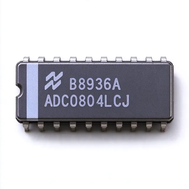
The Texas Instruments ADC0804LCJ is an 8-bit successive-approximation (SAR) analog-to-digital converter in a 20-pin ceramic DIP (CDIP) package, delivering a maximum sampling rate of 10 kSPS with a 100 µs conversion cycle, a 0–5 V (or ±5 V) pseudo-differential input range, an on-chip clock generator needing only an external RC network, and a tri-state 8-bit parallel µP-compatible data interface. It operates from a single 4.5 V to 6.3 V supply (typical 5 V) across an industrial -40°C to +85°C temperature range. The part is active in the market with 2,387 units in stock at XAIPART and MOQ of 1, priced at $11.25 per unit at qty 1, dropping to $6.5625 at qty 1000 as of 2026-11-02. This guide covers how to design it in, its verified pinout, drop-in alternatives within the ADC080x family, and sourcing strategy. For the full product listing, see the ADC0804LCJ product page, or browse the broader XAIPART component catalog.
What Is the ADC0804LCJ and Why Do Engineers Still Specify It?
The ADC0804LCJ is a complete 8-bit data acquisition front end on a single IC. TI designed the ADC0801-05 family for direct microprocessor bus interface without external latches, bus drivers, or an external clock oscillator. The LCJ suffix identifies the ceramic DIP package with the -40°C to +85C industrial temperature grade, distinguishing it from the ADC0804LCN (plastic DIP, 0°C to +70°C) and the ADC0804LCWM (SOIC-20 wide-body, surface mount).
The verified specification set is compact but complete for slow-to-moderate industrial acquisition:
| Parameter | Value |
|---|---|
| Resolution | 8 bits |
| Architecture | SAR (Successive Approximation) with differential potentiometric ladder |
| Sampling Rate (Max) | 10 kSPS |
| Conversion Time | ~100 µs per 8-bit conversion |
| Inputs | 1 single-ended (pseudo-differential) |
| Input Voltage Range | 0 V to 5 V, or ±5 V with ±5 V supplies |
| Data Interface | Parallel (µP-compatible), tri-state 8-bit output |
| Supply Voltage (VCC) | 4.5 V to 6.3 V (typ. 5 V) |
| Reference | External, REF/2 input; ratiometric operation supported |
| Operating Temperature | -40°C to +85°C |
| Package | 20-CDIP (0.300 inch, 7.62 mm), through-hole |
Takeaway: If your requirement is 8-bit resolution, sub-10 kSPS sampling, and a 5 V through-hole part with a wide industrial temperature range, the ADC0804LCJ remains a one-chip answer.
How Do You Design In the ADC0804LCJ? A Practical Technical Guide
Clock generation: one resistor and one capacitor
The ADC0804LCJ includes an on-chip clock generator, so no crystal or oscillator is required. Per the TI datasheet, a 10 kΩ resistor plus 100 pF capacitor on the CLK IN and CLK R pins produces approximately 640 kHz, which is internally divided to clock the SAR at the correct rate for the 100 µs conversion cycle. This is the standard configuration for the entire ADC0801-05 family.
Wiring the analog input
The analog front end uses pins 6 (VIN+) and 7 (VIN-) as a pseudo-differential pair. For single-ended 0–5 V operation, drive VIN+ with your signal and tie VIN- to analog ground. The differential potentiometric ladder architecture rejects common-mode noise on the VIN- node, which matters when the sensor sits at the end of long industrial wiring. For ±5 V bipolar operation, the datasheet supports operation with ±5 V supplies and a bipolar reference arrangement.
Reference and ratiometric measurement
Reference configuration is external via the VREF/2 pin (pin 17) and VREF pin (pin 20). For ratiometric systems — for example, a resistive bridge excited from the same 5 V rail — tie the reference to the bridge excitation voltage. This cancels absolute reference accuracy as an error term, because the ADC output is a ratio of input to reference rather than an absolute measurement.
µP bus interface and timing
Three control pins manage the interface:
- WR (pin 3, active low) — a falling edge on WR starts a conversion.
- INTR (pin 5, active low) — asserts when conversion completes, usable as a polled status line or a microprocessor interrupt.
- RD (pin 2, active low) — reading the data also clears INTR and readies the part for the next conversion.
The tri-state DB0–DB7 outputs connect directly to an 8-bit data bus shared with memory and other peripherals, gated by CS (pin 1). TI's design intent was a turnkey ADC for 8051, Z80, 68HC11, and PIC bus daughter cards with no glue logic — no external sample-and-hold is needed either, since the part integrates one on-chip.
What the minimum external component count looks like
A working acquisition channel needs: the ADC0804LCJ, one 10 kΩ resistor and one 100 pF capacitor for the clock, bypass capacitors on VCC, and the reference arrangement (a divider or direct tie depending on your span). That is the whole analog channel — a key reason the part remains a staple in education labs and breadboard prototypes.
Takeaway: Budget one RC pair for the clock, connect VIN- differentially for noise rejection, and use ratiometric referencing wherever the sensor and reference share an excitation source.
What Is the ADC0804LCJ Pinout?
The 20-pin DIP pinout is standard across the ADC080x family, so replacements swap without rewiring. The functionally critical pins are below; the complete pin table lives on the product page.
| Pin | Name | Function |
|---|---|---|
| 1 | CS | Chip select (active high) |
| 2 | RD | Read strobe (active low) |
| 3 | WR | Write strobe (active low); starts conversion |
| 4 | CLK IN | External clock input / RC network node |
| 5 | INTR | Interrupt output (active low); conversion complete |
| 6 | VIN+ | Analog input, positive (single-ended or differential+) |
| 7 | VIN- | Analog input, negative (ground reference) |
| 8–15 | DB0–DB7 | Tri-state 8-bit parallel data output (DB0 = LSB, DB7 = MSB) |
| 16 | GND | Ground (0 V reference for digital logic) |
| 17 | VREF/2 | Reference voltage / 2 input (sets input range center) |
| 18 | VCC | Positive supply, +4.5 V to +6.3 V (typ. +5 V) |
| 19 | CLK R | Clock RC timing resistor node |
| 20 | VREF | Positive reference voltage input |
Takeaway: Pin-compatible throughout the ADC080x DIP family — pin 1 is CS, pin 3 starts conversions via WR, and pins 6/7 form the differential analog input pair.
Which Alternatives Can Replace the ADC0804LCJ?
All verified alternatives come from the same ADC080x family and share the identical 8-bit SAR core and 10 kSPS timing. The selection differences are package, temperature grade, and linearity.
| Parameter | ADC0804LCJ | ADC0801LCN | ADC0802LCWM | ADC0805LCN |
|---|---|---|---|---|
| Resolution | 8 bits | 8 bits | 8 bits | 8 bits |
| Architecture | SAR | SAR (same core) | SAR (same core) | SAR (same core) |
| Package | 20-CDIP (0.300", 7.62 mm) | 20-PDIP (same footprint) | SOIC-20 (SMD) | 20-PDIP (same footprint) |
| Linearity | ±1 LSB max | ±1/4 LSB max (tighter) | ±1/2 LSB max | ±1 LSB max, with VREF/2 internal |
| Drop-in vs LCJ (DIP) | — | Yes, pin-to-pin | No — different footprint (SMD) | Yes, pin-to-pin |
Selection guidance from the verified data:
- ADC0801LCN — best linearity of the group at ±1/4 LSB max; a drop-in electrical upgrade in the same 20-pin DIP footprint if your circuit tolerates the looser ADC0804 linearity.
- ADC0805LCN — same ±1 LSB linearity and DIP footprint, with an internal VREF/2 arrangement; effectively interchangeable on the ADC side.
- ADC0802LCWM — identical SAR core in a SOIC-20 wide-body surface-mount package; use for new PCB layouts and volume production, but it is not footprint-compatible with the ceramic DIP.
- ADC0804LCN — identical electrical specifications and pinout in plastic DIP rated 0°C to +70°C; the lowest-cost true drop-in when the industrial temperature range is not required.
- Microchip parts — Microchip does not make a pin-compatible drop-in. Its cross-reference tool lists functionally similar SPI ADCs such as MCP3001 and MCP3002, but these require PCB redesign and firmware changes.
Takeaway: For a true drop-in, choose ADC0801LCN (tighter linearity), ADC0805LCN (same grade with internal VREF/2), or ADC0804LCN (commercial temperature, lower cost). Switch to the LCWM SOIC only when you control the PCB layout.
What Is the Supply and Pricing Situation for the ADC0804LCJ?
The ADC0804LCJ is listed as an active part in the XAIPART database, with 2,387 units in stock and a minimum order quantity of 1. Verified XAIPART pricing as of 2026-11-02 is:
| Quantity | Unit Price (USD) |
|---|---|
| 1–9 | $11.25 |
| 10–99 | $8.125 |
| 100–499 | $7.1875 |
| 500–999 | $6.875 |
| 1000+ | $6.5625 |
Authorized distribution includes DigiKey, Mouser, Heisener, and Octopart-listed suppliers. For design continuity, note that ceramic DIP parts like the LCJ are legacy-package products typically used in industrial maintenance and repair stock; the price spread between qty 1 ($11.25) and qty 1000 ($6.5625) is roughly 42%, so consolidating buys materially reduces unit cost. Check current stock on the ADC0804LCJ product page before committing to a BOM quantity.
Takeaway: Stock is available now at 2,387 units with MOQ 1; buy at the 100-piece tier ($7.1875) or above for the best unit economics on sustained production or spares pools.
Where Does the ADC0804LCJ Fit in Real Designs? Six Verified Use Cases
- Industrial process control data acquisition — Digitize a 4–20 mA loop signal conditioned to 0–5 V through a 250 Ω sense resistor, sampled at 100 Hz by a process controller. The pseudo-differential input and ratiometric reference reject common-mode noise from sensor wiring, and the -40°C to +85°C range handles factory-floor environments. The parallel output connects directly to legacy 8051, Z80, and 68xx microcontrollers without glue logic.
- Legacy digital panel meters and DVM front ends — The 8-bit resolution (≈0.4% steps) supports 3.5/4.5-digit panel-meter readouts, and the 100 µs conversion cycle easily covers the 2–3 readings-per-second typical DPM update rate. The ceramic DIP of the LCJ is preferred for long-life industrial instruments.
- Sensor signal-conditioning digitization — Thermocouple, RTD, strain gauge, and humidity front ends output into the 0–5 V input range. The 10 kSPS rate covers vibration and acoustic sensing below 4 kHz signal bandwidth, and the on-chip clock saves an oscillator in compact sensor modules.
- Microprocessor-compatible interface boards — Tri-state outputs, CS, and the INTR handshake were designed for direct µP bus daughter cards; the ADC shares a bus with memory and other peripherals, polled or interrupt-driven.
- Educational labs and breadboard prototyping — The through-hole 20-pin DIP fits standard solderless breadboards, and the minimal external parts (one RC clock, bypass caps, reference divider) let students focus on SAR theory. The parallel output drives LED bargraphs or logic analyzers directly.
- Audio VU metering and slow-signal digitization — For rectified audio level metering in vintage equipment restoration, 8 bits at 10 kSPS is sufficient, and the internal sample-and-hold eliminates a fast external T/H amplifier.
Takeaway: Every verified application shares one profile — one analog channel, slow-to-moderate bandwidth, 5 V rail, and a parallel-capable controller. If your design matches that profile, the LCJ fits.
Worked Design: A 4–20 mA Process-Loop Digitizer Channel
Problem: Digitize a 4–20 mA industrial transmitter loop into an 8-bit microcontroller at 100 Hz with industrial temperature capability.
Approach: Convert the loop current to voltage with a 250 Ω sense resistor: 4 mA × 250 Ω = 1.000 V and 20 mA × 250 Ω = 5.000 V, which maps directly onto the ADC0804LCJ's verified 0–5 V input range at a 5 V supply. Drive VIN+ from the sense resistor and connect VIN- to analog ground near the resistor to exploit the pseudo-differential input's common-mode rejection. Use the standard 10 kΩ + 100 pF RC on CLK IN/CLK R for the ~640 kHz clock. Reference the ADC from the same 5 V rail for ratiometric operation.
Timing check: One conversion takes ~100 µs. Sampling at 100 Hz consumes only 1% of the converter's 10 kSPS capability, leaving enormous margin for oversampling and averaging to improve effective resolution.
Interface: Pulse WR low to start each conversion; poll INTR (active low) or wire it to the MCU interrupt input; assert RD with CS to latch DB0–DB7 into the controller port. No latches, no bus drivers, no external sample-and-hold.
Result: A complete industrial acquisition channel in one IC plus three passive components, operating -40°C to +85°C in a breadboard-friendly ceramic DIP. At 1000-piece quantities the channel costs $6.5625 in converter cost as of 2026-11-02.
Takeaway: A 250 Ω sense resistor maps the 4–20 mA loop exactly onto the ADC0804LCJ's verified 0–5 V span — no gain stage required.
What Should Buyers Watch Next for the ADC0804LCJ?
Three trends anchor this part's sourcing outlook:
- Through-hole availability is the constraint. The LCJ's value is its 20-CDIP through-hole format with -40°C to +85C rating — a combination modern SMD ADCs do not replicate pin-to-pin. If your repair or maintenance strategy depends on DIP, keep the ADC0801LCN and ADC0805LCN (same footprint) qualified as alternates while the part is active.
- RoHS status needs verification for new designs. Ceramic DIP legacy parts historically shipped in lead-finish variants for industrial customers; for new RoHS-required designs, the plastic-DIP ADC0804LCN is the recommended substitute per the verified distributor guidance. Confirm the current declaration on the official TI ADC0804 datasheet.
- Linearity upgrades are free wins. Because the ADC0801LCN offers ±1/4 LSB max linearity versus the ADC0804's ±1 LSB max in the identical DIP footprint, new designs in this family should default to the ADC0801 grade unless sourcing drives otherwise.
For adjacent design reading, see our guide to the NE5534ADRG4 low-noise op-amp for front-end amplification ahead of the ADC input, the C8051F061 mixed-signal MCU guide for modern controllers with integrated ADCs, and more component deep-dives on the XAIPART blog.
Takeaway: Qualify ADC0801LCN/ADC0805LCN as DIP alternates now; move new RoHS-driven designs to the LCN plastic-DIP grade; and exploit the tighter-linearity ADC0801 grade in new layouts.
التعليقات
كن أول من يعلّق.
🔐 يرجى تسجيل الدخول لنشر تعليق.
ليس لديك حساب؟ إنشاء حساب