ADC/DAC
المنتجات (2,700+)

AD9049BR - 9-Bit 30 MSPS ADC | Analog Devices
The Analog Devices AD9049BR is a 9-bit monolithic sampling analog-to-digital converter with an onboard track-and-hold circuit and reference, a maximum sampling rate of 30 MSPS, a single analog input, and a 28-pin SOIC package. It is designed for low-cost, high-performance signal-conversion applications that require only a +5 V supply and an encode clock. The digital outputs are CMOS, while the encode clock is TTL compatible and supports both 5 V and 3.3 V operation. An ADC is a data-acquisition and signal-conversion integrated circuit that converts a continuous or sampled analog voltage into a digital code. Within the semiconductor hierarchy, the AD9049 is a sampling ADC, a data-converter IC, and a member of the broader ADC/DAC product category. Its 9-bit resolution provides 512 possible digital output codes and is appropriate for waveform capture, communications, instrumentation, and embedded control applications where a compact converter and direct digital output are more important than very high resolution. The AD9049BR combines the sampling mechanism, track-and-hold function, and internal reference in one monolithic device. According to the official Analog Devices product page, only +5 V power and an encode clock are required to achieve 30 MSPS operation. The encode clock provides sampling timing, while the CMOS output bus presents the converted digital result to a capture or processing system. The specified 5 V and 3.3 V clock compatibility expands its usefulness in mixed-voltage digital designs. This converter is appropriate for industrial digital instrumentation, communication receivers, control and monitoring systems, embedded signal capture, and test equipment. Its onboard track-and-hold and reference reduce the number of external analog functions required for basic sampling systems. Designers should still budget appropriate acquisition bandwidth, input drive, clock quality, bypass capacitance, output timing margin, and PCB signal-integrity control. For AD9049BR designs, the most important trade-off is the relationship between its 9-bit resolution and 30 MSPS throughput. The converter provides fast sampling and direct digital outputs, but it does not offer the fine quantization of a higher-resolution ADC. Application-specific input range, voltage, timing, and pin details were not present in the supplied verification data and must be confirmed in the manufacturer datasheet before layout or firmware is finalized. This page consolidates current manufacturer and distributor findings, verified pricing references, same-package candidate availability, and practical design guidance. It distinguishes confirmed AD9049BR facts from parameters that require datasheet verification, helping engineers identify gaps before committing a board layout or production BOM.

AD9051BRSRL - 10-Bit 60 MSPS Pipelined ADC | Analog Devices
The Analog Devices AD9051BRSRL is a 10-bit monolithic sampling analog-to-digital converter (ADC) with an integrated track-and-hold (T/H) amplifier and on-chip voltage reference, packaged in a 28-pin SSOP (5.30 mm body width) and shipping in Tape & Reel format. The device delivers 60 MSPS sampling rate with 9.3 effective number of bits (ENOB) at 10.3 MHz input and consumes only 250 mW of total power at full 60 MSPS rate, all from a single +5 V supply. It uses a pipelined architecture fabricated on a BiCMOS process to balance high dynamic performance against low cost. An analog-to-digital converter (ADC) is a mixed-signal integrated circuit that samples a continuous analog input and converts it to a discrete digital code at a defined sample rate. Within the converter taxonomy, the AD9051 falls into the pipeline ADC category - pipelined sub-family - which sits between flash converters (faster but power-hungry) and successive-approximation ADCs (lower power but slower). Pipeline ADCs are the workhorses of mid-bandwidth communications, instrumentation, and imaging systems. The 60 MSPS / 10-bit combination places the AD9051 in the entry-to-mid range of that family, where cost, ENOB, and power efficiency matter more than absolute speed. Key features include a selectable input bandwidth of 50 MHz or 130 MHz (user-selectable via a logic pin), a single +5 V supply requirement, and a built-in sample-and-hold that eliminates the need for an external front-end T/H. The reference is also internal, which simplifies PCB layout and reduces bill-of-materials cost. Industrial-temperature-range operation (-40 C to +85 C) and SSOP packaging allow the part to be used in dense, surface-mount designs where 28-pin dual-inline footprints are too tall. The AD9051's pipelined architecture samples on a clock edge, then processes each stage through low-resolution sub-ADCs and DACs, with inter-stage gain and digital error correction. The BiCMOS process allows fast analog sampling with low digital leakage, supporting 9.3 ENOB at 10.3 MHz input; this is more than adequate for video-rate and IF-sampling digitizers. The internal reference is trimmed at the factory, removing the need for an external reference and the associated routing noise. Typical applications include ultrasound imaging front ends, IF-sampling communication receivers, CCD/imaging camera digitizers, and low-cost instrumentation digitizers. The 50/130 MHz selectable bandwidth makes it equally usable for narrow-band IF strips and wider baseband signals such as composite video. The 250 mW power budget is friendly to fanless medical and industrial enclosures. When designing with the AD9051, run the encode clock from a low-jitter source and decouple AVDD and DVDD close to the pins. The selectable input bandwidth pin should be tied high or low before conversion begins; glitching this pin during operation can corrupt samples. Drive the analog input through a wideband op-amp with at least 100 MHz gain-bandwidth product for full-Nyquist linearity. This page combines distributor pricing, drop-in alternative parts, and design notes - a synthesis not found in the standalone AD9051 datasheet.
AD9051BRSRL-2V - 10-Bit 60 MSPS ADC, 28-SSOP | Analog Devices
The Analog Devices AD9051BRSRL-2V is a 10-bit monolithic sampling analog-to-digital converter (ADC) with a maximum sample rate of 60 MSPS, an onboard track-and-hold amplifier, and an internal voltage reference, housed in a 28-pin SSOP package and supplied on a 7-inch tape-and-reel. The part is specified over the industrial temperature range (-40C to +85C) and operates from a single +5 V analog supply; the digital outputs are CMOS-compatible and can be configured for either 5 V or 3 V logic levels, while the encode clock input is TTL-compatible. An analog-to-digital converter is a data-acquisition building block that converts a continuous-time analog input into a discrete digital code at a sampling clock rate, and belongs to the broader hierarchy of mixed-signal IC -> ADC -> pipelined/flash ADC -> semiconductor. The two-step (sub-ranging) architecture used in the AD9051 is optimized to deliver the best dynamic performance available while still keeping total power dissipation low, which makes it a popular choice for cost-driven designs that still need solid spurious-free dynamic range and signal-to-noise ratio. Key specifications include 60 MSPS sampling rate, 9.3 effective number of bits (ENOB) at fIN = 10.3 MHz, 250 mW total power consumption at 60 MSPS, a user-selectable input bandwidth of either 50 MHz or 130 MHz, and on-chip track-and-hold plus voltage reference. The internal T/H relaxes front-end analog driver requirements and the integrated reference eliminates an external reference component, reducing both BOM count and board area in cost-sensitive designs. Typical applications for the AD9051BRSRL-2V include digital video, professional CCD imaging, digital oscilloscopes, low-cost digital still cameras, portable instrumentation, and IF-sampling communication receivers where the selectable input bandwidth simplifies front-end anti-alias filter design. When laying out the PCB, keep the analog input traces short and use a solid ground plane; the encode clock should be routed with controlled impedance and kept away from the analog inputs to preserve SNR.

AD9054ABSTZ-200 - 8-Bit 200 MSPS ADC | Analog Devices
The Analog Devices AD9054ABSTZ-200 is an 8-bit monolithic analog-to-digital converter (ADC) optimized for high speed, low power, small size, and ease of use. Delivering a 200 MSPS guaranteed encode rate and a 350 MHz full-power analog bandwidth, the part is housed in a 44-pin LQFP (10x10 mm) package with exposed thermal pad. It operates from a single +5 V analog supply plus an ECL/LVDS-compatible clock, with an internal 2.5 V reference and an internal track-and-hold (T/H) front end. An ADC (analog-to-digital converter) is a mixed-signal integrated circuit that converts a continuous-time analog voltage or current into a discrete digital code word at a defined sample rate. Within the converter hierarchy, ADCs sit beneath data converters, which are themselves part of the signal chain IC family. 8-bit, >100 MSPS converters such as the AD9054A target applications where high sample rate and wide analog bandwidth matter more than bit depth, including IF sampling, instrumentation, digital oscilloscope front ends, and digital data-acquisition recorders. Key features of the AD9054ABSTZ-200 include 200 MSPS guaranteed conversion rate, 350 MHz analog input bandwidth, 1 V p-p analog input range for ease of interface, integrated dual-port architecture (per Analog Devices datasheet), and low power consumption relative to competitive 8-bit solutions. Per the Analog Devices datasheet, SNR is approximately 47 dB at 200 MSPS and SFDR is about 53 dB, with aperture delay and aperture jitter tightly controlled to support time-domain imaging. Operating temperature range is -40C to +85C, making the ADC suitable for industrial environments. Architecture-wise, the part is built on a bipolar process using an internal pipelined topology with error-correction logic across the first stages, paired with an on-chip reference and T/H. This combination reduces external component count and removes the need for external reference buffers. The LQFP-44 footprint has a Gull-Wing lead finish and supports standard SMT reflow profiles. Typical applications include IF sampling in communications receivers, digital oscilloscope and digitizer front ends, medical imaging signal paths (ultrasound / MRI baseband), radar preprocessing in defense and aerospace hardware, and high-speed data acquisition in test-and-measurement equipment. The 44-LQFP (STZ) package enables straightforward four-layer PCB layouts with controlled-impedance clock routing. When designing with the AD9054ABSTZ-200, source-terminate the clock at the driver and provide a clean analog ground plane tied through a single star point to the digital return, because the 350 MHz analog bandwidth makes the device very sensitive to ground bounce. Decouple AVDD with a 0.1 uF ceramic plus 10 uF tantalum placed within 5 mm of each supply pin, and verify SFDR is not degraded by the chosen clock source jitter (per the Analog Devices datasheet, jitter should remain below 0.5 ps RMS for full performance). This page synthesizes distributor pricing, drop-in same-family alternatives from Analog Devices, and verified cross-brand web-data equivalents - going beyond a basic datasheet reprint to support sourcing and design decisions.

AD9057BRS-60 - 8-Bit 60MSPS ADC | Analog Devices
Analog Devices AD9057BRS-60 is an 8-bit monolithic analog-to-digital converter (ADC) optimized for low cost, low power consumption, small package size, and ease of use. It supports up to 60 MSPS encode rate in the BRS-60 speed grade, with the same die also offered in 40 MSPS (BRS-40) and 80 MSPS (BRS-80) grades. The part integrates a 120 MHz full-power analog input bandwidth track-and-hold amplifier, an internal +2.5 V reference, and a single +5 V supply LDD-style digital interface, all housed in a 20-pin SSOP (RS-20) package. An 8-bit ADC is a converter that quantizes an analog input signal into 256 discrete digital codes (2^8) at a specified sample rate. In the broader taxonomy, the AD9057 belongs to flash / pipelined ADCs (sub-category of data converters), which sit inside signal-chain ICs and ultimately under analog/mixed-signal ICs. ADCs of this class are typically used as the front-end digitizer between a sensor or analog conditioning stage and a digital ASIC, FPGA, or DSP that performs further processing. Key features of the AD9057BRS-60 include 200 mW typical power dissipation at full sample rate, a 10 mW power-down mode for portable/battery applications, an on-chip 2.5 V reference that eliminates an external reference IC, 1 V p-p analog input range, single +5 V analog supply operation, and 3 V logic interface compatibility. The 120 MHz analog input bandwidth comfortably exceeds the 60 MSPS Nyquist requirement, allowing gentle anti-alias filter design and supporting undersampling IF architectures. The integrated track-and-hold minimizes aperture jitter and sample-rate-dependent phase error. Architecturally, the AD9057 is implemented as an 8-bit flash ADC with a front-end sample-and-hold and on-chip reference. The flash architecture gives single-cycle latency (one clock of pipeline delay is sometimes quoted for the pipelined grade) and excellent dynamic performance for repetitive or single-shot digitizations. Encoding logic is TTL/CMOS-compatible, allowing direct connection to a 5 V-tolerant FPGA or 3.3 V logic without level shifters in most cases. Typical applications include digital oscilloscopes, professional video digitizers, CCD/camera signal processing, medical ultrasound receive paths, cable modem upstream/downstream QAM demodulators, and general-purpose data-acquisition front ends. The 60 MSPS grade is the balanced middle option of the family: it provides more headroom than 40 MSPS for wide-bandwidth signals while consuming less power than the 80 MSPS grade. Design tip: keep the analog input trace impedance-controlled (typically 50 ohm or 75 ohm) and place a termination resistor at the ADC input pin to damp the track-and-hold kick-back; add small RC anti-alias filtering ahead of the input. Decouple VDD with 0.1 uF and 10 uF ceramic capacitors placed within 5 mm of the supply pins. This page synthesizes distributor pricing, drop-in same-package alternatives, and practical design notes that go beyond what the manufacturer datasheet provides alone.
AD9057BRSRL60SP211 - 8-Bit 60MSPS ADC, 20-SSOP | Analog Devices
The Analog Devices AD9057BRSRL60SP211 is an 8-bit monolithic analog-to-digital converter (ADC) operating at 60 MSPS encode rate, housed in a 20-pin SSOP package. It is part of the AD9057 family which offers 40 MSPS, 60 MSPS, and 80 MSPS speed grades, with a full-power analog input bandwidth of 120 MHz. The SRL60SP211 suffix encodes the 60 MSPS grade and the 20-SSOP packaging on tape-and-reel. According to the AD9057 product page, this converter is optimized for low cost, low power, small size, and ease of use. An analog-to-digital converter (ADC) is a mixed-signal integrated circuit that samples a continuous-time analog voltage at discrete intervals and quantizes each sample into a digital code. ADCs sit at the boundary between the analog front end (sensors, amplifiers, anti-alias filters) and the digital signal processing back end (FPGA, ASIC, microcontroller). The hierarchy places this part as: flash-style or two-step ADC -> ADC -> data converter -> mixed-signal IC -> semiconductor. Low-cost 8-bit ADCs like the AD9057 are commonly used in image processing, video digitizing, IF sampling communications, and instrumentation, where 60 dB of dynamic range and tens-of-MHz bandwidth are sufficient. Key features include single +5 V analog supply operation, low power consumption (typically <250 mW at 60 MSPS), TTL-compatible outputs, an internal +2.5 V reference, and a single-ended analog input. The 120 MHz analog bandwidth allows the part to under-sample IF signals or sample baseband signals with wide bandwidth. The 20-pin SSOP package is a thin shrink small-outline surface-mount package that is footprint-compatible across the AD9057 40/60/80 MSPS speed grades, enabling PCB reuse when board designers need to switch speed grades. The AD9057 architecture uses an internal track-and-hold front end followed by a 2-step flash quantizer, achieving 8-bit linearity without requiring external sample-and-hold or reference components. Encode (clock) inputs are TTL/CMOS compatible, and the digital outputs are 3-state TTL outputs for direct connection to an FPGA, ASIC, or backplane. The internal +2.5 V reference can be driven externally for system-wide calibration or left unconnected to use the internal reference as default. Typical applications include professional and consumer video digitizing, image processing front ends for line-scan or area-scan cameras, low-cost digital oscilloscope input stages, IF sampling for low-IF radios, and instrumentation data acquisition. The 60 MSPS grade is selected when designers need to balance sample rate against cost without paying for the 80 MSPS headroom. When designing with the AD9057BRSRL60SP211, pay attention to the analog input network: a 50 ohm termination followed by an AC-coupling capacitor and a bias network is typical, with an anti-alias filter preceding the ADC input. Decouple AVDD and DVDD with 0.1 uF ceramic capacitors placed as close to the pins as possible. Leave the exposed pad (where applicable) soldered to the ground plane for thermal dissipation. This page synthesizes verified distributor pricing, same-brand drop-in alternatives, and practical design notes not found in the manufacturer datasheet alone.

AD90585 - Dual 8-Bit 50 MSPS ADC | Analog Devices
The AD90585 is a dual 8-bit analog-to-digital converter (ADC) from Analog Devices, designed for high-speed data acquisition in communications and instrumentation systems. It integrates two independent 8-bit ADCs on a single monolithic IC, each capable of conversion rates up to 50 MSPS. The device includes an optional on-board voltage reference, simplifying system design and reducing external component count. The AD90585 operates from ±5V power supplies and features a flexible input range, making it suitable for a variety of signal conditioning topologies. An analog-to-digital converter (ADC) is a critical building block in digital signal processing chains, converting continuous analog signals into discrete digital values for processing by microcontrollers, DSPs, or FPGAs. The AD90585 belongs to the family of high-speed flash ADCs, which use a parallel comparator architecture to achieve very high sampling rates. This architecture is ideal for applications requiring wide bandwidth and low latency, such as radar, communications, and medical imaging. Key features of the AD90585 include two matched ADCs on a single chip, ensuring excellent channel-to-channel matching for applications like quadrature demodulation. The device offers a low power consumption of less than 1W, making it suitable for portable and power-sensitive designs. The low input capacitance of 10 pF minimizes loading on the driving amplifier, preserving signal integrity. The on-board voltage reference provides a stable and accurate reference, eliminating the need for an external reference in many designs. The AD90585 uses a flash architecture with a resistor ladder and comparator bank, achieving high-speed conversion with minimal latency. The device includes a reference ladder offset feature, which uses 2 kΩ pull-down resistors on the output data bits to equalize rise and fall times at high conversion rates, easing data latching into external logic. This design consideration is critical for reliable operation above 40 MSPS. Typical applications include quadrature demodulation for communications, digital oscilloscopes, and other high-speed data acquisition systems. The dual-channel architecture is particularly advantageous in I/Q demodulation, where two matched ADCs are required to process in-phase and quadrature components simultaneously. The low power and small footprint make it suitable for embedded systems and portable instrumentation. When designing with the AD90585, ensure that the analog input is properly buffered and that the reference ladder offset resistors are included for high-speed operation. The device requires careful PCB layout to minimize parasitic capacitance and maintain signal integrity. The ±5V supplies should be well-decoupled to avoid noise coupling into the analog input.
AD9058AJJ - Dual 8-Bit 50 MSPS ADC | Analog Devices | JLCC-44
The Analog Devices AD9058AJJ is a dual 8-bit 50 MSPS analog-to-digital converter that integrates two independent high-performance flash ADCs on a single monolithic IC, housed in a 44-pin JLCC (J-lead ceramic chip carrier) package measuring 16.39 x 16.39 mm. Each ADC channel supports up to 50 MSPS conversion rate with optimized dynamic performance (SNR and ENOB), and an optional onboard +2 V voltage reference can drive both ADCs for unipolar positive 0 V to +2 V input operation. An ADC (analog-to-digital converter) is a data converter integrated circuit that samples continuous analog signals and quantizes them into discrete digital codes for downstream DSP, storage, or transmission. The AD9058AJJ is a flash-architecture dual ADC - flash converters use a parallel bank of comparators to perform conversion in a single clock cycle, achieving the highest sampling speed among ADC architectures at the cost of higher power consumption and silicon area. As a dual device, the AD9058AJJ belongs to the data converter IC family within mixed-signal semiconductor products. Key features include 50 MSPS sampling rate per channel, 8-bit resolution, two independent ADC channels on one die, an optional internal +2 V reference, low input capacitance, and a wide analog input bandwidth supporting video and IF-sampling applications. The 44-pin JLCC hermetic package supports both commercial (0 C to +70 C) and military (-55 C to +125 C) temperature ranges for harsh-environment systems. The flash architecture eliminates the need for external sample-and-hold circuits in many applications, and the dual-channel integration reduces board space, BOM count, and channel-to-channel skew in I/Q or dual-channel data acquisition paths. With a single -5.2 V analog supply and TTL-compatible digital outputs, the AD9058AJJ interfaces directly to standard logic families. Typical applications include digital oscilloscopes, medical imaging front-ends, radar and sonar signal processing, I/Q demodulation for communications, professional video digitizers, and any dual-channel high-speed data acquisition system requiring matched ADC channels on a single substrate. When designing with this device, provide a low-impedance analog ground plane and decouple supplies close to the package; mismatch between the two ADC channels can be exploited for I/Q applications but must be characterized for matched-path designs. This page synthesizes distributor pricing, parametric drop-in alternatives, and practical design notes not consolidated in the manufacturer datasheet.

AD9058JJ - Dual 8-Bit 50 MSPS ADC | Analog Devices
Analog Devices AD9058JJ is a dual 8-bit analog-to-digital converter with two independent converters, a maximum conversion rate of 50 MSPS, and an optional onboard +2 V voltage reference in a 44-pin J-lead ceramic package. The two converter channels provide a cost-effective way to acquire two related analog signals in communications, instrumentation, and signal-processing systems. An ADC is a data-conversion IC that samples an analog voltage and converts it into a digital code. A flash-type ADC performs conversion through parallel comparison and encoding networks, making it appropriate for high-speed sampling where latency and throughput are important. The AD9058 belongs to the ADC/DAC category, within the broader data-converter and semiconductor hierarchy. Key features include two matched ADCs on one monolithic IC, operation at up to 50 MSPS, low input capacitance of 10 pF, and power consumption below 1 W. The flexible input range supports both unipolar and bipolar signal arrangements when the appropriate circuitry is used. The optional internal reference can drive both converters and can establish a 0 V to +2 V unipolar operating range. The monolithic dual-converter architecture reduces the need for two separate ADC packages while preserving independent analog inputs and digital outputs. A common device and matched channels are useful when sampling quadrature signals or monitoring two channels that must be acquired coherently. Input capacitance of 10 pF lowers the burden placed on source drivers, while the 50 MSPS ceiling supports communication demodulation, digital oscilloscopes, and other sampled-data systems. Typical uses include quadrature demodulation in communications, digital oscilloscopes, digital communications receivers, instrumentation, and control systems. The internal reference can simplify system design when an external precision reference is unnecessary, but external references may be preferred when multiple converters must share an especially stable reference. Designers should account for input bandwidth, settling time, source impedance, clock jitter, and analog supply requirements when selecting input circuitry. Decoupling should follow the manufacturer datasheet recommendations, and unused converter channels should be configured according to the prescribed interface and power-state sequence. This page consolidates the verified manufacturer description, lifecycle information, pricing references, family alternatives, and application guidance into an engineering-oriented resource for evaluating the AD9058JJ in dual-channel high-speed acquisition systems.
AD9066AR - Dual 6-Bit 60 MSPS ADC | Analog Devices
The Analog Devices AD9066AR is a dual 6-bit, 60 MSPS monolithic analog-to-digital converter with two matched ADCs, a single +5 V supply, and CMOS-compatible digital I/O in a 28-lead SOIC package. It combines a 400 mW low-power dissipation rating with an on-chip voltage reference and self-biased inputs for AC-coupled signals. An ADC is a mixed-signal data-converter IC that samples an analog voltage and produces a corresponding digital code. The AD9066 belongs to the flash-converter family, with parallel digital outputs designed for high-speed waveform capture and signal processing. Its dual architecture supports simultaneous conversion of two channels, including the in-phase and quadrature components found in RF demodulators. The AD9066AR offers two independent 6-bit conversion channels operating at up to 60 MSPS. Each channel provides six bits of resolution, while the matched converters support phase-sensitive I/Q measurement. The converter uses a single +5 V supply and CMOS-compatible output interface, allowing its digital outputs to connect directly to compatible FPGA, DSP, or data-capture logic when voltage and timing requirements are satisfied. The on-chip voltage reference provides a stable basis for converter calibration and reduces the need for an external reference circuit. For AC-coupled analog inputs, the self-biased input arrangement centers the signal near midscale with low offset. This feature simplifies the interface when the source is transformer-coupled or AC-coupled through a blocking capacitor, while the source impedance and settling requirements still need to be checked in the complete signal chain. The AD9066 was optimized for low-cost in-phase and quadrature demodulators, particularly digital direct-broadcast satellite receivers using QPSK modulation. It can also suit communications, RF instrumentation, feedback control, and other systems that need two synchronized high-speed sampling paths, provided that 6-bit resolution is adequate for the required signal-to-noise ratio. For layout, place input, reference, and decoupling connections according to the Analog Devices datasheet, minimizing trace length and keeping analog and digital return paths controlled. The 60 MSPS operating rate requires careful clock and output timing design; do not assume that a connector or FPGA interface is compatible solely because both use single-ended CMOS signals. This product page consolidates the verified AD9066AR operating data, sourcing information, package constraints, and application guidance. It also distinguishes orderable variants from genuine pin-compatible replacements so engineers can make a defensible board-level sourcing decision without confusing different package or reel codes with functional alternatives.
AD9066JR - Dual 6-Bit 60 MSPS ADC | Analog Devices
The Analog Devices AD9066JR is a dual 6-bit monolithic analog-to-digital converter optimized for low-cost in-phase and quadrature demodulation, with a conversion rate of 60 MSPS, 400 mW power dissipation, a single +5 V supply, and a 28-pin SOIC package. It converts two simultaneous analog signals into six-bit digital outputs while providing CMOS-compatible digital interfaces for downstream demodulation and processing. An ADC is a data-conversion IC that samples an analog voltage and represents it as a digital code. Within the signal-chain hierarchy, the AD9066 is a dual flash ADC: a dual analog-to-digital converter, a data converter, a signal-processing IC, and ultimately a semiconductor. Its paired I and Q channels support coherent quadrature demodulation, while its relatively low resolution reduces output logic and digital-processing demands compared with higher-resolution converters. Key features include two matched ADCs on one CMOS-compatible chip, 6-bit resolution, operation to 60 MSPS, a single +5 V analog supply, and CMOS-compatible outputs rated for 60 MSPS. The on-chip voltage reference biases the analog inputs to midscale, and the self-biased architecture supports AC-coupled inputs. The manufacturer identifies direct broadcast satellite receivers and QAM demodulators as primary applications. The AD9066JR commercial-grade version is specified for 0°C to +70°C operation. The AD9066 uses flash conversion to acquire high-speed samples without requiring a separate reference and ADC core for each channel. Two matched converters on one die help maintain matching between the in-phase and quadrature paths, which is important when phase and amplitude relationships carry information. Digital outputs are CMOS-compatible, while the encode input uses a CMOS stage with a TTL-compatible 1.4 V threshold. These interfaces allow the converter to be paired with external digital demodulators, processors, or FPGAs. Typical uses include direct broadcast satellite receivers, QAM demodulators, broadband quadrature phase-shift-keying receivers, communications receivers, and other sampled I/Q systems where 6-bit resolution is sufficient. The 60 MSPS sampling rate supports high-bandwidth signal acquisition, while the 28-pin SOIC package supports conventional surface-mount assembly and compact single-board construction. Designers should verify analog input range, common-mode behavior, required input coupling, digital output timing, and output encoding against the manufacturer datasheet before layout. Because the converter operates at 60 MSPS, controlled clock routing, low-impedance analog returns, adequate bypass capacitance, and separation of analog and digital return currents are important. The commercial temperature range also makes the AD9066JR unsuitable for applications requiring the broader industrial range of the AD9066AR. This page consolidates the verified manufacturer specifications, distributor pricing, package and temperature distinctions, substitution limits, and application guidance. It also distinguishes verified facts from unspecified electrical details, avoiding unsupported claims where complete pin-level or timing information was not present in the retrieved source material.
AD9070BR - 10-Bit 100 MSPS ECL ADC | Analog Devices
The Analog Devices AD9070BR is a monolithic 10-bit sampling analog-to-digital converter with a 100 MSPS conversion rate, an on-chip track-and-hold circuit, and ECL digital interfaces. It consumes 600 mW typical at 100 MSPS, provides 230 MHz analog input bandwidth, and accepts a 1 V p-p analog input range in a ceramic DIP package. A sampling ADC is a data-conversion IC that samples an analog voltage at a controlled instant and converts that sample into a digital code. The AD9070 belongs to the ADC and DAC product hierarchy, where it functions as a high-speed parallel-output converter. Its 100 MSPS throughput supports wideband signal acquisition while its 230 MHz analog bandwidth allows sampling signals above the converter's Nyquist frequency when used with suitable filtering. The AD9070's primary characteristics include 10-bit resolution, 100 MSPS conversion, 600 mW typical power at 100 MSPS, a 1 V p-p analog input range, and ECL-compatible digital outputs. Its on-chip track-and-hold circuitry reduces the need for external sample-and-hold components. The manufacturer also identifies an on-chip reference and a differential clock input as standard features. This converter combines an on-chip reference with an integrated sampling structure and ECL interface. ECL output levels are suited to high-speed digital systems that require fast data transfer, although the receiving logic, clock distribution, supply arrangement, and termination network must be designed carefully. According to the Analog Devices product page, the AD9070 operates over its full operating range with outstanding dynamic performance. Typical applications include broadband communications test equipment, digital oscilloscope and waveform-analysis front ends, radar or electronic-surveillance signal acquisition, high-speed instrumentation, and communications receivers. The 230 MHz analog bandwidth is especially useful when the input path must preserve high-frequency content, while the 100 MSPS conversion rate determines the maximum real-time sampling bandwidth. The main design consideration is that this is a high-speed, single-supply converter rather than a general-purpose low-voltage ADC. Layout must minimize clock and analog-input ringing, provide suitable input and reference decoupling, and route the 10-bit ECL output with controlled impedance. The exact ceramic-DIP pinout and full application circuit should be checked against the manufacturer datasheet before layout release. This page consolidates verified manufacturer information, distributor availability, pricing, technical comparisons, and engineering guidance. It also distinguishes documented AD9070BR capabilities from unverified substitute and pinout information so that procurement and design decisions can be made without treating inferred data as confirmed specifications.
AD9071BR - 10-Bit, 100 MSPS ADC | Analog Devices
Analog Devices AD9071BR is a 10-bit, 100 MSPS monolithic sampling analog-to-digital converter with an on-chip track-and-hold circuit, a 280 MHz analog input bandwidth, and TTL/CMOS-compatible digital outputs in a 28-lead plastic SOIC package. The converter operates from a single 5 V supply and requires an encode clock for full-performance operation. A sampling ADC is an analog-to-digital converter that uses an internal track-and-hold circuit to capture an input voltage before conversion. It belongs to the ADC hierarchy, which forms part of data-converter and signal-processing semiconductors. The AD9071 combines sampling, quantization, an internal reference, and parallel digital output in one device, allowing analog signals to be digitized for subsequent digital processing. The principal features include 10-bit resolution, a maximum conversion rate of 100 MSPS, low power operation at 100 MSPS, an on-chip track-and-hold circuit, and an on-chip reference. The analog input range is 1 V peak-to-peak, while the digital interface supports TTL-compatible 5 V or 3.3 V output operation. Its 280 MHz analog bandwidth is well above the 100 MSPS conversion rate, providing bandwidth for input signals and sampling requirements. The AD9071 uses a parallel digital output architecture rather than a serial interface. This allows captured words to be transferred directly into digital logic, buffers, DSPs, or programmable logic when their timing interfaces are compatible. The 28-lead package provides separate digital data and control connections, but the verified source excerpts supplied for this record do not include a complete pin-number-to-function table. Typical applications include digital communications, signal-intelligence systems, and other high-speed signal-processing installations. The device is particularly relevant where a sampling rate of 100 MSPS, 10-bit resolution, and a 1 V peak-to-peak input range are required without the complexity of a serial-output converter interface. Designers should treat the single 5 V analog supply and the encode clock as central to circuit planning. Input conditioning must provide a suitable 1 V peak-to-peak signal, while clock and digital-interface timing must be controlled to preserve conversion performance. The complete manufacturer datasheet should be used to verify pin functions, input common-mode requirements, output timing, and recommended application circuitry. This page consolidates the verified manufacturer descriptions, available distributor references, package information, selection trade-offs, and practical design guidance for AD9071BR. It also clearly separates confirmed parameters from information that was not supplied, avoiding unsupported electrical or replacement claims.

AD9081BBCZ - Quad 16-Bit 12GSPS RF DAC & 12-Bit 4GSPS ADC | Analog Devices
The AD9081BBCZ is a highly integrated mixed signal front end (MxFE) from Analog Devices, combining a quad, 16-bit, 12 GSPS RF digital-to-analog converter (DAC) core and a quad, 12-bit, 4 GSPS RF analog-to-digital converter (ADC) core. This device is designed for wideband communication systems, radar, and test and measurement applications, offering exceptional dynamic range and bandwidth. The AD9081 features a 16-lane, 24.75 Gbps JESD204C or 15.5 Gbps JESD204B serial interface, enabling high-speed data transfer to FPGAs and ASICs. The device is packaged in a 324-ball BGA-ED (15x15 mm) package, providing excellent thermal and electrical performance. A mixed signal front end (MxFE) is a single-chip solution that integrates high-speed data converters with analog front-end circuitry, such as amplifiers, filters, and mixers, to interface directly with RF signals. In the signal chain hierarchy, the MxFE sits between the antenna and the digital baseband processor, replacing multiple discrete components with a single, highly integrated device. This integration reduces board space, power consumption, and design complexity while improving performance by minimizing parasitic effects and signal degradation. Key features of the AD9081 include a 16-bit DAC with a maximum sample rate of 12 GSPS, a 12-bit ADC with a maximum sample rate of 4 GSPS, and a flexible digital signal processing (DSP) chain with programmable decimation and interpolation filters. The device supports multiple operating modes, including single-band and multi-band configurations, and offers a wide input frequency range up to 5 GHz for the ADC and output frequency range up to 7 GHz for the DAC. The AD9081 also includes an integrated clock multiplier, phase-locked loop (PLL), and digital up/down converters, simplifying system design. The AD9081 utilizes advanced BiCMOS process technology, achieving high linearity and low noise performance. The DAC features a spurious-free dynamic range (SFDR) of [DATA_NEEDED: SFDR] dBc, while the ADC achieves a signal-to-noise ratio (SNR) of [DATA_NEEDED: SNR] dBFS. The device operates from a 1.0 V core supply and 1.8 V I/O supply, with a total power dissipation of [DATA_NEEDED: power dissipation] W. The JESD204C interface supports subclass 1 deterministic latency, ensuring precise synchronization across multiple devices. Typical applications include 5G massive MIMO base stations, phased array radar, electronic warfare, and broadband test and measurement equipment. The AD9081's high sample rates and wide bandwidth make it ideal for direct RF sampling architectures, eliminating the need for multiple downconversion stages. In 5G systems, the device enables the digitization of entire frequency bands, simplifying the radio design and improving flexibility. When designing with the AD9081, careful attention must be paid to power supply decoupling and clock jitter, as these directly impact the converter's dynamic performance. The device requires a clean, low-jitter clock source, and the use of high-quality bypass capacitors is essential. Additionally, the thermal management of the 324-ball BGA package should be considered, as the device can dissipate significant power at high sample rates.

AD9172BBCZ - Dual 16-Bit 12.6 GSPS RF DAC | Analog Devices
The AD9172BBCZ is a high-performance, dual, 16-bit digital-to-analog converter (DAC) from Analog Devices, designed for direct-to-RF wireless applications. It supports DAC sample rates up to 12.6 GSPS and features an 8-lane, 15 Gbps JESD204B data input port, an on-chip DAC clock multiplier, and advanced digital signal processing (DSP) capabilities for single-band and multiband signal generation. The device is housed in a 144-ball BGA-ED (10x10 mm) package, offering a compact solution for high-density RF systems. A digital-to-analog converter (DAC) is an electronic component that converts digital data into an analog signal. In RF applications, a high-speed DAC like the AD9172 enables direct synthesis of radio frequency signals, eliminating the need for multiple upconversion stages. This reduces system complexity, power consumption, and board space. The AD9172 belongs to the family of RF DACs, which are specialized data converters optimized for generating signals in the gigahertz frequency range, often used in software-defined radios, radar, and communications infrastructure. Key features of the AD9172 include dual 16-bit DAC cores, a maximum sample rate of 12.6 GSPS, and an integrated JESD204B interface supporting up to 15 Gbps per lane. The on-chip clock multiplier allows flexible clocking from lower-frequency references, simplifying system design. The device also includes digital upconversion (DUC) and channelizer blocks, enabling multiband operation and reducing the digital processing load on FPGAs or ASICs. These features make the AD9172 ideal for applications requiring wide instantaneous bandwidth and high spectral purity. From a technical perspective, the AD9172 leverages advanced CMOS process technology to achieve high-speed operation while maintaining excellent dynamic performance. The DAC architecture includes a current-steering core with integrated output matching, providing a differential output that can drive RF transformers or amplifiers directly. The device supports multiple operating modes, including real and complex output, and offers programmable interpolation filters to optimize signal quality. The JESD204B interface simplifies high-speed data transfer, reducing the number of digital I/O pins compared to parallel interfaces. Typical applications for the AD9172 include wireless base stations, radar systems, electronic warfare, and test and measurement equipment. In wireless infrastructure, the device enables direct RF synthesis for 5G NR and LTE signals, supporting carrier aggregation and MIMO configurations. In radar, the high sample rate and wide bandwidth allow generation of complex waveforms for improved target detection. The device is also suitable for software-defined radio platforms, where flexibility and performance are critical. When designing with the AD9172, careful attention must be paid to power supply decoupling and clock jitter, as these directly impact the output signal quality. The device requires multiple supply rails, and proper filtering is essential to achieve the specified noise and spurious performance. Additionally, the JESD204B interface must be configured correctly to ensure reliable data transfer, and the reference clock should be generated from a low-jitter source to minimize phase noise.
AD9173BBCZ - Dual 16-Bit 12.6 GSPS RF DAC | Analog Devices
The AD9173BBCZ is a high-performance, dual, 16-bit digital-to-analog converter (DAC) from Analog Devices, designed for demanding RF and wideband applications. It supports DAC sample rates up to 12.6 GSPS and features an 8-lane, 15.4 Gbps JESD204B data input port, enabling high-speed data transfer from FPGAs or ASICs. The device integrates a high-performance on-chip DAC clock multiplier and advanced digital signal processing (DSP) capabilities, including channelizers, making it ideal for single-band and multiband radio architectures. A digital-to-analog converter (DAC) is a device that converts digital signals into analog voltages or currents. In RF systems, high-speed DACs like the AD9173 are essential for generating wideband waveforms directly at radio frequencies, eliminating the need for multiple upconversion stages. The AD9173 belongs to the family of RF transceivers and data converters, which are critical components in modern communication systems, radar, and test equipment. Key features of the AD9173BBCZ include dual 16-bit DACs, a maximum sample rate of 12.6 GSPS, and a JESD204B interface with 8 lanes at 15.4 Gbps. The on-chip clock multiplier allows the use of a lower-frequency reference clock, simplifying system design. The device also offers a flexible digital upconversion (DUC) engine with multiple channelizers, supporting both single-band and multiband operation. These features enable direct RF synthesis, reducing system complexity and power consumption. From a technical perspective, the AD9173 utilizes a high-speed CMOS DAC core with advanced interpolation filters and numerically controlled oscillators (NCOs). The JESD204B interface supports subclass 1 deterministic latency, ensuring precise synchronization in multi-chip systems. The device operates from a 1.0V core supply and 1.8V/3.3V I/O supplies, with power dissipation typically around 2.5W at full sample rate. The 144-ball BGA-ED package (10x10 mm) provides excellent thermal performance and signal integrity for high-frequency operation. Typical applications for the AD9173BBCZ include wireless infrastructure (4G/5G base stations), radar systems, electronic warfare, and test and measurement equipment. Its high sample rate and wide bandwidth make it suitable for generating wideband signals in software-defined radios and direct RF sampling architectures. The device's multiband capability allows a single DAC to generate multiple carriers simultaneously, reducing component count and cost. When designing with the AD9173, careful attention must be paid to power supply decoupling and clock jitter. Use low-noise LDOs for analog supplies and a high-quality clock source to achieve optimal SNR and SFDR. The JESD204B interface requires proper termination and impedance matching to ensure error-free data transfer at 15.4 Gbps.
AD9174BBCZ - 16-Bit 12.6 GSPS RF DAC | Analog Devices
The AD9174BBCZ is a high-performance, dual, 16-bit digital-to-analog converter (DAC) from Analog Devices that supports DAC sample rates up to 12.6 GSPS. Housed in a 144-BGA-ED (10x10) surface-mount package, the device embeds an 8-lane JESD204B data input port running at up to 15.4 Gbps per lane, an on-chip DAC clock multiplier, and digital signal processing optimized for single-band and multiband direct-to-radio-frequency (RF) wireless applications. An RF DAC is a data converter that directly synthesizes analog RF signals from digital baseband or IF data, removing multiple analog upconversion stages. In the signal chain hierarchy, the AD9174BBCZ functions as a digital-to-analog converter within the broader data converter IC family, and it is often paired with RF transceivers, FPGAs, and clock generators. The 16-bit resolution combined with 12.6 GSPS update rate enables wide instantaneous bandwidth for modern communication and radar waveforms. Key features include dual independent DAC channels, 16-bit resolution, maximum DAC sample rate of 12.6 GSPS, JESD204B input interface supporting 8 lanes at 15.4 Gbps, and a high-performance on-chip clock multiplier. The integrated DSP provides flexible interpolation, NCO, and digital upconversion functions that allow direct RF signal generation from L-band through C-band and above, depending on the clocking configuration. From an architecture perspective, the AD9174BBCZ integrates a programmable interpolator, digital upconverter, and numerically controlled oscillator (NCO) with the high-speed DAC core. This reduces the amount of external logic and programmable fabric required in the transmit path. The device is designed for dense multi-band deployments where low power, high output bandwidth, and excellent spectral performance are critical. Typical applications include 5G/6G wireless infrastructure, radar and electronic warfare systems, satellite communications, and high-performance test and measurement instrumentation. The combination of 12.6 GSPS sampling and 15.4 Gbps JESD204B lanes allows a single device to serve both single-band and multiband direct-to-RF architectures. When designing with this device, pay close attention to the reference clock quality, JESD204B link configuration, and PCB layout for the high-speed serial lines. The on-chip DAC clock multiplier reduces external clock component count but requires a clean low-jitter reference to achieve rated SFDR and phase noise performance.
AD9220AR - 12-Bit 10 MSPS Monolithic ADC | Analog Devices
The Analog Devices AD9220AR is a 12-bit, 10.0 MSPS monolithic analog-to-digital converter with one pipelined input in a 28-lead SOIC package. According to the verified manufacturer result, it operates from a single +5 V supply and belongs to the AD9221, AD9223, and AD9220 family, whose devices share interface options, package, and pinout. Its headline specifications are 12-bit resolution, 10.0 MSPS maximum sampling performance, and 28-SOIC packaging. An ADC is an integrated circuit that samples an analog input voltage and converts it into a digital code for processing, measurement, control, or communication. The AD9220AR uses a pipelined ADC architecture, which supports conversion speed and resolution while requiring multiple clock cycles to complete a conversion. Its single input and parallel data interface make it suitable for systems where a fixed, fast conversion rate is more important than multiplexing many channels. The verified product information identifies flexible sampling rates of 1.5 MSPS, 3.0 MSPS, and 10.0 MSPS, with low power dissipation values of 59 mW, 100 mW, and 250 mW corresponding to those operating modes. The family is specified as a complete 12-bit monolithic converter with true 12-bit linearity and temperature-drift performance. The AD9220AR is therefore useful when a design needs reproducible acquisition performance, a 5 V analog supply, and a conventional parallel digital interface. Technically, the device is designed as a single-supply, high-speed sampling ADC. The +5 V supply simplifies analog power planning, while the 28-lead SOIC package supports conventional surface-mount assembly. Designers should pay attention to the distinction between the family’s multiple sampling-rate options: the target MPN is specifically associated with the 10.0 MSPS class. Input conditioning, clock quality, grounding, and digital-interface timing remain essential for realizing the converter’s rated performance. Typical applications include industrial measurement, communications signal capture, instrumentation, digital oscilloscope and waveform-acquisition systems, and embedded data-acquisition modules. The converter can be paired with a microcontroller, FPGA, DSP, or other digital controller when serialized data storage, filtering, and system-level memory are required. The AD9220 family pin compatibility also permits upgrading among related family members when performance requirements change. A key design consideration is to use the manufacturer datasheet’s recommended analog input, reference, supply, and decoupling arrangements. Keep sensitive analog traces away from digital switching nodes, use a controlled clock source, and account for acquisition timing and settling before treating a conversion as valid. Do not infer pin functions from the package name; consult the complete datasheet pinout for the AD9220AR. This page combines verified manufacturer specifications, distributor listing information, lifecycle status, and same-package family comparison data. It distinguishes documented AD9220 family compatibility from unverified substitute claims and avoids presenting missing electrical details as established specifications.
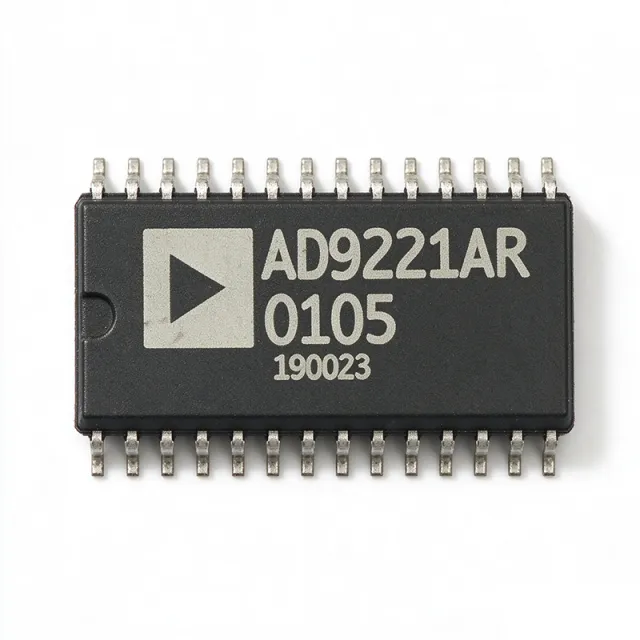
AD9221AR - 12-Bit 1.5 MSPS ADC, 28-SOIC | Analog Devices (Tape & Reel)
The Analog Devices AD9221AR is a monolithic 12-bit, 1.5 MSPS (mega-samples per second) single-supply analog-to-digital converter (ADC) housed in a 28-pin SOIC (Small Outline IC) wide-body package. It features pipelined architecture with true 12-bit linearity, 11.5-bit or better AC performance, and parallel digital output. The wide SOIC package (0.295 inch / 7.50 mm body width) provides robust thermal performance and ease of hand-soldering during prototyping, while tape-and-reel packaging enables high-volume automated assembly. An ADC (analog-to-digital converter) is a semiconductor device that transforms continuous analog voltage signals into discrete digital codes at a defined sampling rate. Within the signal chain hierarchy, the ADC sits between the analog front end (sensor, amplifier, anti-alias filter) and the digital processing block (DSP, FPGA, microcontroller). The 12-bit resolution places the AD9221 in the precision-conversion tier, delivering 4096 discrete output codes (LSB = VREF/4096) suitable for instrumentation, communications, and industrial control where 0.024% quantization steps are acceptable. Key features of the AD9221AR include flexible sampling rates (the AD9221 family spans 1.5, 3.0, and 10.0 MSPS across AD9221/AD9223/AD9220), low power dissipation (a critical advantage for portable and densely-populated designs), on-chip sample-and-hold, and a single +5 V supply operation. The device is pin-compatible with the higher-speed AD9223 (3 MSPS) and AD9220 (10 MSPS), allowing designers to scale sampling rate up or down without PCB rework. The pipelined architecture uses multiple low-resolution stages with inter-stage DACs and digital error correction, producing high throughput at moderate power. A precision bandgap reference and flexible input configuration support both single-ended and differential drive schemes, while the parallel CMOS-compatible digital interface simplifies connection to FPGAs, ASICs, or microcontrollers. Internal calibration ensures specified linearity over temperature. Typical applications include medical imaging (ultrasound front-end digitization), communications IF sampling, instrumentation and test equipment, industrial process control loops, CCD digitizers, and sonar/radar signal processing. Its combination of 12-bit precision with mid-rate sampling suits applications where higher-resolution SAR converters are too slow but full 14-16 bit pipelines are unnecessary. When designing with the AD9221AR, use a low-impedance input buffer (such as the AD8138 or AD8055) to drive the analog inputs, and place the reference bypass capacitor close to the REFCOM and VREF pins. Decouple AVDD and DRVDD separately to prevent digital switching noise from coupling into the analog front end. The wide SOIC footprint allows easy inspection and rework, an advantage for prototype builds. This page synthesizes distributor stock and pricing, drop-in same-family alternatives (AD9220/AD9223), and practical design notes not collected in any single location on the manufacturer datasheet.
AD9221AR-REEL - 12-Bit 1.5 MSPS ADC, 28-SOIC | Analog Devices
The Analog Devices AD9221AR-REEL is a monolithic 12-bit, 1.5 MSPS (mega-samples per second) single-supply analog-to-digital converter (ADC) housed in a 28-pin SOIC (Small Outline IC) wide-body package. It features pipelined architecture with true 12-bit linearity, 11.5-bit or better AC performance, and parallel digital output. The wide SOIC package (0.295 inch / 7.50 mm body width) provides robust thermal performance and ease of hand-soldering during prototyping, while tape-and-reel packaging enables high-volume automated assembly. An ADC (analog-to-digital converter) is a semiconductor device that transforms continuous analog voltage signals into discrete digital codes at a defined sampling rate. Within the signal chain hierarchy, the ADC sits between the analog front end (sensor, amplifier, anti-alias filter) and the digital processing block (DSP, FPGA, microcontroller). The 12-bit resolution places the AD9221 in the precision-conversion tier, delivering 4096 discrete output codes (LSB = VREF/4096) suitable for instrumentation, communications, and industrial control where 0.024% quantization steps are acceptable. Key features of the AD9221AR-REEL include flexible sampling rates (the AD9221 family spans 1.5, 3.0, and 10.0 MSPS across AD9221/AD9223/AD9220), low power dissipation (a critical advantage for portable and densely-populated designs), on-chip sample-and-hold, and a single +5 V supply operation. The device is pin-compatible with the higher-speed AD9223 (3 MSPS) and AD9220 (10 MSPS), allowing designers to scale sampling rate up or down without PCB rework. The pipelined architecture uses multiple low-resolution stages with inter-stage DACs and digital error correction, producing high throughput at moderate power. A precision bandgap reference and flexible input configuration support both single-ended and differential drive schemes, while the parallel CMOS-compatible digital interface simplifies connection to FPGAs, ASICs, or microcontrollers. Internal calibration ensures specified linearity over temperature. Typical applications include medical imaging (ultrasound front-end digitization), communications IF sampling, instrumentation and test equipment, industrial process control loops, CCD digitizers, and sonar/radar signal processing. Its combination of 12-bit precision with mid-rate sampling suits applications where higher-resolution SAR converters are too slow but full 14-16 bit pipelines are unnecessary. When designing with the AD9221AR-REEL, use a low-impedance input buffer (such as the AD8138 or AD8055) to drive the analog inputs, and place the reference bypass capacitor close to the REFCOM and VREF pins. Decouple AVDD and DRVDD separately to prevent digital switching noise from coupling into the analog front end. The wide SOIC footprint allows easy inspection and rework, an advantage for prototype builds. This page synthesizes distributor stock and pricing, drop-in same-family alternatives (AD9220/AD9223), and practical design notes not collected in any single location on the manufacturer datasheet.
AD9225AR - 12-Bit 25 MSPS ADC | Analog Devices
The Analog Devices AD9225AR is a monolithic 12-bit, 25 MSPS analog-to-digital converter with an on-chip sample-and-hold amplifier and voltage reference, supplied in a 28-pin SOIC W package. It operates from a single +5 V supply and has a typical power dissipation of 280 mW, making it suitable for compact, high-speed signal-acquisition systems that require parallel digital output. An ADC is a data-conversion IC that samples an analog voltage and converts it into a numeric value. The AD9225 belongs to the pipelined ADC family, a multistage architecture commonly used for conversion rates from tens of megasamples per second to hundreds of megasamples per second. Within the broader semiconductor hierarchy, it is an analog-to-digital converter, data-converter IC, signal-processing IC, and mixed-signal semiconductor. Key features include a 12-bit resolution, a 25 MSPS conversion rate, a guaranteed maximum differential nonlinearity error of 0.4 LSB, and guaranteed no missing codes. The converter includes both its sample-and-hold amplifier and voltage reference on chip, reducing the number of external analog components required. Its parallel output architecture supports direct connection to FPGA, CPLD, or data-capture logic for deterministic sampling throughput. The AD9225 uses a multistage differential pipelined architecture and supports a differential input arrangement with VIN and VINB connections. The manufacturer datasheet recommends centering the analog-input common-mode voltage at approximately 2.5 V by driving VINB from a low-impedance 2.5 V source. With the VREF pin connected directly to SENSE, the reference voltage is 1 V and the corresponding input span is 2 V p-p; the stated valid input-signal range is 1.5 V to 3.5 V. Typical uses include industrial process monitoring, communications infrastructure, digital oscilloscopes, radar and sonar signal chains, waveform capture, and precision control loops. The AD9225 is especially appropriate when 25 MSPS sampling is sufficient and parallel output provides an advantage over serial-interface converters. Its integrated sample-and-hold and reference functions simplify board design while the single +5 V supply reduces multi-rail complexity. The main design trade-off is input bandwidth and signal integrity at 25 MSPS. Differential routing, controlled impedance, a low-noise +5 V supply, proper reference decoupling, and careful return-path management are essential for preserving full-scale accuracy. Engineers should also account for digital-output timing when routing 12 parallel data bits plus clock signals into acquisition logic. This page consolidates the verified manufacturer specifications, current distributor availability, family pin-compatibility information, practical application guidance, and parameter-level replacement analysis. It is designed to help engineers determine whether the AD9225AR fits their acquisition architecture before purchasing or redesigning the board.
AD9226ARS - 12-Bit 65 MSPS ADC | Analog Devices
The Analog Devices AD9226ARS is a 12-bit, 65 MSPS analog-to-digital converter with an on-chip high-performance sample-and-hold amplifier and voltage reference, supplied in a 28-pin SSOP package. It is designed for data-acquisition systems requiring parallel digital output and single-supply operation. The verified product data identifies a monolithic, single-channel, pipelined ADC with differential analog inputs and no missing codes. An ADC is an integrated circuit that converts an analog voltage into a digital numerical value. The AD9226 belongs to the data-converter hierarchy and specifically uses a multistage differential pipeline architecture. Its 65 MSPS sampling rate supports high-speed signal capture, while 12-bit resolution provides 4096 possible digital codes. The internal sample-and-hold amplifier acquires the analog input, and the on-chip voltage reference supports repeatable conversion without requiring a separate reference device. Key features include 12-bit resolution, a 65 MSPS data rate, a single analog input channel, differential input architecture, and parallel output. The converter is specified as a single-supply device. The verified manufacturer listing also describes low-power dissipation and no-missing-code operation. These characteristics make the AD9226ARS suitable for communications, instrumentation, industrial control, test equipment, and other applications where sampled analog waveforms must be digitized rapidly. The AD9226 architecture uses a multistage differential pipeline to implement the conversion. This structure separates the conversion process into successive stages, allowing high throughput compared with a single-stage flash converter. The differential input arrangement can improve rejection of common-mode noise when the source is balanced and the analog front end is correctly implemented. The output interface is parallel, so system designers must account for the timing and routing of the data lines. Typical applications include communications receivers, radar and signal-processing systems, test and measurement instruments, medical instrumentation, industrial process monitoring, and embedded data-acquisition systems. In each case, the input bandwidth, conversion rate, reference accuracy, digital interface, and package availability must be checked against the system requirements before design release. The primary design consideration is ensuring that the analog input bandwidth and external circuitry match the 65 MSPS conversion rate. The sample-and-hold amplifier, voltage reference, power supply, clocking, and digital timing should be evaluated according to the manufacturer datasheet. This page summarizes verified product information and identifies specification fields that require confirmation from the current Analog Devices datasheet.
AD9226ARSZ - 12-Bit 65 MSPS Pipeline ADC | Analog Devices
The Analog Devices AD9226ARSZ is a monolithic, single-supply, 12-bit, 65 MSPS analog-to-digital converter featuring an on-chip high-performance sample-and-hold amplifier and internal voltage reference, housed in a 28-pin SSOP package. It delivers a differential input range and 65 MSPS conversion rate, consuming only a few hundred milliwatts from a single +5 V supply. An analog-to-digital converter (ADC) is a data converter that transforms continuous analog signals into discrete digital codes for processing by DSPs, FPGAs, and microcontrollers. Pipeline ADCs like the AD9226 use multiple low-resolution flash stages to achieve high sample rates with low latency; they sit within the hierarchy of successive-approximation (SAR), delta-sigma, and flash ADCs, and belong to the broader data-converter family of mixed-signal ICs used in signal-chain and instrumentation systems. Key features include a signal-to-noise ratio of approximately 69 dB, a spurious-free dynamic range (SFDR) of approximately 80 dB, an effective number of bits (ENOB) of 11.1 at fIN = 10 MHz, and a low-power architecture aimed at imaging and communications front-ends. The wideband sample-and-hold input supports differential or single-ended drive with simple passive or active signal conditioning, and the digital outputs provide CMOS-compatible parallel data. Internally the AD9226 uses a multistage differential pipeline architecture with output error-correction logic. The on-chip 2.5 V reference can be left internal or overdriven by an external reference for gain calibration or channel matching in multi-board systems; the data-ready output simplifies interface to FIFOs, DSPs, and FPGAs. Typical applications include medical ultrasound imaging, IF sampling in communications receivers, baseband digital signal processing, instrumentation digitizers, and CCD/camera imaging systems. The combination of 12-bit resolution, 65 MSPS sampling rate, and 28-SSOP footprint makes it a versatile front-end for mid-bandwidth data acquisition. When designing with the AD9226, the most important consideration is using a single +5 V supply rail and providing proper analog input common-mode biasing; bypassing the supply pins with 100 nF and 10 uF ceramic capacitors placed within a few millimetres of each pin maintains rated dynamic performance and minimizes digital coupling into the analog front-end. This page synthesizes distributor pricing, drop-in same-package alternatives, and practical design notes not found in the manufacturer datasheet, helping engineers shorten the selection and PCB procurement cycle.
AD9226ARSZRL - 12-Bit 65 MSPS Parallel ADC | Analog Devices
The Analog Devices AD9226ARSZRL is a 12-bit, single-channel, 65 MSPS pipelined analog-to-digital converter with a parallel data interface, an integrated voltage reference, and an on-chip sample-and-hold amplifier, packaged in a 28-lead SSOP. An ADC converts an analog voltage into a digital code for processing, instrumentation, communications, or control. The AD9226 belongs to the pipelined ADC family and uses multiple internal stages to achieve high sampling rates while balancing resolution, power, and design complexity. Its 12-bit resolution provides 4096 code levels, while the 65 MSPS sampling rate supports high-speed signal capture. The parallel interface exposes digital conversion results through dedicated output pins and is suitable for systems whose downstream logic can accept the required data timing. Key features include a single-supply architecture, a high-performance sample-and-hold amplifier, an integrated voltage reference, and a multistage differential pipeline. The verified manufacturer information identifies a 65 MSPS data rate, 12-bit resolution, one analog input, and a parallel data interface. The AD9226 also uses CMOS technology and is specified for an industrial temperature range of -40°C to +85°C. Its 28-pin SSOP package is intended for surface-mount assembly, and the AD9226ARSZRL ordering code uses tape-and-reel packaging. The converter is suitable for communications receivers, IF undersampling systems, baseband measurements, industrial signal acquisition, and embedded test equipment. Its pipeline architecture is particularly appropriate when a system needs predictable throughput and digital timing rather than the flexibility of a low-power successive-approximation ADC. The on-chip reference and sample-and-hold amplifier reduce the number of external analog functions required in a basic capture circuit. A key design consideration is the relationship between sampling rate, analog bandwidth, settling behavior, and downstream digital timing. The parallel outputs must be captured correctly by an external FPGA, ASIC, or other digital controller, while the analog input network must provide adequate impedance, bandwidth, and signal integrity. The AD9226ARSZRL is a fixed-function converter, so system flexibility must be provided by the surrounding analog and digital circuitry. Pricing and availability should be checked with authorized distributors as of 2026-10-22 because distributor inventory and lead time can change. This page combines verified manufacturer specifications, distributor listings, package information, and application-oriented design guidance. It also distinguishes confirmed drop-in alternatives from unverified cross-reference candidates so engineers can avoid treating a similar specification as proof of pin compatibility.