ADC/DAC
Produtos (2364)

5962-0423001QXC - 14-Bit 80 MSPS Military ADC QML Q | Analog Devices
The Analog Devices 5962-0423001QXC is a high-speed, high-performance monolithic 14-bit analog-to-digital converter (ADC), also known as the AD6645ASQ/QMLQ, housed in a 52-lead thermally-enhanced hermetic ceramic QFP package. The device is 100% production tested at 70 MHz analog input and 150 MHz at -35C to +85C case temperature, providing guaranteed dynamic performance across military temperature ranges. The SMD part number 5962-0423001QXC indicates QML Q qualification per MIL-PRF-38535, making it suitable for high-reliability defense and aerospace applications. What is an ADC? An Analog-to-Digital Converter is a mixed-signal integrated circuit that samples continuous analog input voltages and converts them into discrete digital codes. The 5962-0423001QXC uses a pipelined multibit architecture to achieve 80 MSPS sampling rates, falling within the high-speed ADC product category. Pipelined ADCs are the technology of choice for IF sampling, radar receivers, and digital oscilloscopes where both speed and resolution are required. Key features include 14-bit resolution, 80 MSPS maximum sample rate, ENOB of approximately 11.5 bits at Nyquist input, and SFDR exceeding 80 dBc. The integrated input buffer simplifies the front-end analog interface, eliminating the need for an external ADC driver in many cases. The device operates from a single 3.3V analog supply and 3.3V digital supply with separate grounds for noise isolation. The 5962-0423001QXC uses a fully differential architecture with a pipelined, multibit-per-stage core to balance speed, linearity, and power consumption. The on-chip input buffer handles the switched-capacitor input structure, while a digital error correction circuit removes missing-code errors. The QML Q qualification ensures the part meets Defense Logistics Agency (DLA) requirements for space, missile, and avionics systems. Typical applications include phased-array radar receivers, electronic countermeasures (ECM) systems, secure communication links, signals intelligence (SIGINT) platforms, and high-speed instrumentation. The wide input bandwidth supports IF sampling in software-defined radio (SDR) systems, eliminating aliasing-prone downconversion stages. When designing with this part, allocate adequate copper area for the thermal pad to maintain junction temperature below the maximum rating. The hermetic ceramic package requires careful thermal management for long-term reliability in vibration environments. Always follow the DLA-qualified manufacturer listing (QML) guidelines during PCB layout, derating, and screening procedures. This page synthesizes distributor pricing, military-grade alternatives, and design guidance drawn from Analog Devices datasheets not found on a single distributor summary.

5962-85127023A - 12-Bit SAR ADC, 28-LCC | Analog Devices
The 5962-85127023A is a military-grade, 12-bit successive-approximation analog-to-digital converter (ADC) manufactured by Analog Devices Inc. It is the SMD (Standard Microcircuit Drawing) version of the AD574A, a complete 12-bit ADC with 3-state output buffer circuitry for direct interface to an 8- or 16-bit microprocessor bus. The device features a single input channel, a SAR architecture, and is packaged in a 28-lead ceramic leadless chip carrier (28-LCC) measuring 11.43x11.43 mm. It includes an on-chip high-precision voltage reference and clock, guaranteeing full-rated performance without external circuitry or clock signals. An analog-to-digital converter (ADC) is an electronic component that converts continuous analog signals into discrete digital numbers. The SAR (successive-approximation register) architecture is a popular ADC topology that performs a binary search through all possible quantization levels before converging on the final digital output. This ADC belongs to the data acquisition subsystem, which is a critical part of any digital signal processing chain, bridging the analog world to digital processors. The 5962-85127023A is designed for high-reliability applications, particularly in aerospace, defense, and industrial environments where precision and durability are paramount. Key features of the 5962-85127023A include 12-bit resolution, a single-ended input, and a parallel output interface. The device operates from a standard ±12V and +5V power supply, and its internal reference and clock eliminate the need for external components, simplifying design. The 28-LCC package is hermetically sealed, providing excellent protection against moisture and mechanical stress, making it suitable for harsh environments. The device is fully specified over the military temperature range of -55°C to +125°C, ensuring reliable operation in extreme conditions. Technically, the AD574A design uses a precision voltage reference and a successive-approximation register to achieve high accuracy and speed. The 3-state output buffers allow direct connection to a microprocessor bus without additional interface logic, reducing system complexity. The device's conversion time is typically 25 microseconds, providing a throughput of up to 40 kSPS, which is adequate for many industrial and aerospace data acquisition applications. The internal clock ensures consistent conversion timing, and the device can be easily configured for 8-bit or 16-bit bus operation via the 12/8 control pin. Typical applications for the 5962-85127023A include military avionics, radar systems, industrial process control, and test and measurement equipment. Its high reliability and wide temperature range make it ideal for mission-critical systems where failure is not an option. The device's parallel interface simplifies integration with microcontrollers and DSPs, and its internal reference reduces external component count, saving board space and improving system reliability. When designing with this ADC, ensure that the analog input signal is properly buffered and filtered to avoid aliasing and to maintain signal integrity. The power supply should be well-regulated and decoupled with 0.1µF ceramic capacitors close to the device pins. The digital output lines should be terminated appropriately to minimize reflections and noise.

5962-8871901MXA - 12-Bit Quad DAC, 28-CDIP | Analog Devices
The 5962-8871901MXA is a military-grade, 12-bit quad digital-to-analog converter (DAC) from Analog Devices, part of the AD664 family. It integrates four complete voltage-output DACs on a single monolithic IC, housed in a 28-pin ceramic dual-in-line package (CDIP). This device is designed for precision analog output in harsh environments, offering double-buffered input latches and data readback functionality. It operates over the full military temperature range and is compliant with MIL-STD-883, making it suitable for aerospace, defense, and industrial applications. A digital-to-analog converter (DAC) is an electronic component that converts digital binary data into an analog voltage or current. The AD664 is a quad DAC, meaning it contains four independent DAC channels on one chip, each with its own output. This architecture is essential in multi-channel control systems where multiple analog signals must be generated simultaneously, such as in servo control, waveform generation, and automatic test equipment. DACs are a subset of data converters, which also include analog-to-digital converters (ADCs), and are fundamental building blocks in mixed-signal systems. Key features of the 5962-8871901MXA include 12-bit resolution, four DAC channels, and a double-buffered input latch structure that allows simultaneous update of all outputs. The device supports 4-, 8-, or 12-bit parallel word formats, enabling flexible interfacing with a wide range of microprocessors. A reset function clears all registers to a known state, and the data readback feature allows verification of written data. The R-2R ladder architecture ensures monotonicity and low glitch energy. Technically, the AD664 uses a segmented R-2R ladder network for each DAC, providing excellent linearity and low output noise. The double-buffered latches allow the host processor to write to all four DACs independently and then update them simultaneously with a single strobe, which is critical for applications requiring synchronized analog outputs. The device operates from a single +12V supply and provides a bipolar output range of ±10V, with a settling time of typically 10 µs. Typical applications include precision servo control systems, automatic test equipment, and military avionics. The 5962-8871901MXA is also used in industrial process control and instrumentation where multiple analog outputs are needed. Its military-grade qualification ensures reliable operation in extreme temperatures and vibration environments. When designing with this DAC, ensure that the digital supply and analog supply are properly decoupled to minimize noise coupling. The reference input should be driven by a low-impedance source to maintain accuracy. Also, consider the output settling time when designing the update rate of the system.
5962-8965501LA - 12-Bit Military ADC | Analog Devices
The 5962-8965501LA is a 12-bit analog-to-digital converter (ADC) manufactured by Analog Devices, designed for military-grade applications. It features 24 terminals, a wide operating temperature range of -55°C to +125°C, and a fast conversion time of 10.4 microseconds. This device is part of the 5962 series, which is known for high reliability and performance in harsh environments. An analog-to-digital converter (ADC) is a critical component in electronic systems that converts continuous analog signals into discrete digital values for processing by microcontrollers, DSPs, or FPGAs. The 5962-8965501LA is a successive approximation register (SAR) type ADC, which offers a good balance of speed, resolution, and power consumption. It is commonly used in data acquisition systems, industrial control, and military avionics where precision and reliability are paramount. Key features of the 5962-8965501LA include 12-bit resolution, which provides 4096 discrete levels, ensuring high accuracy in signal conversion. The device operates from a 5V supply, making it compatible with standard logic levels. Its military temperature range ensures operation in extreme conditions, and the 10.4 µs conversion time allows for sampling rates up to approximately 96 kSPS, suitable for many real-time applications. Technically, the ADC uses a SAR architecture with an internal sample-and-hold circuit, providing excellent linearity and low power dissipation. The device is packaged in a ceramic DIP (CDIP) or similar hermetic package, ensuring protection against moisture and mechanical stress. The 5962-8965501LA is compliant with MIL-STD-883, a military standard for microcircuits, guaranteeing its robustness and long-term reliability. Typical applications include military radar systems, missile guidance, avionics data acquisition, and industrial process control. Its wide temperature range and high reliability make it ideal for aerospace and defense applications where failure is not an option. When designing with this ADC, ensure proper decoupling of the power supply and reference voltage to minimize noise. The conversion start signal should be synchronized with the system clock to avoid timing errors. Additionally, the digital output should be buffered to drive capacitive loads without degradation.

5962-9078501MLA - 12-Bit Dual DAC, MIL-STD-883 | Analog Devices
The 5962-9078501MLA is a military-grade, 12-bit dual digital-to-analog converter (DAC) manufactured by Analog Devices Inc. It is designed for high-reliability applications requiring precision analog output in harsh environments. The device features two independent DAC channels, each providing a 12-bit resolution with a parallel interface. It operates from dual supplies of ±11.4V to ±15.75V and is packaged in a 24-pin ceramic dual-in-line package (CDIP) with a 0.300-inch (7.62mm) body width. The operating temperature range is -55°C to +125°C, making it suitable for aerospace, defense, and industrial applications. A digital-to-analog converter (DAC) is an electronic component that converts digital binary data into an analog voltage or current. It is a fundamental building block in data acquisition systems, where it translates digital signals from microprocessors or DSPs into real-world analog signals for control, measurement, or audio reproduction. DACs are categorized by resolution (number of bits), speed (conversion rate), and interface type (parallel or serial). The 5962-9078501MLA is a parallel-interface, 12-bit dual DAC, meaning it can simultaneously update two analog outputs from a single digital input bus, which is essential for applications like waveform generation, motor control, and calibration systems. Key features of the 5962-9078501MLA include its dual-channel architecture, which saves board space and reduces component count in multi-channel systems. The device is screened to MIL-STD-883, ensuring it meets stringent military reliability standards for temperature, shock, and vibration. The parallel interface allows for fast data transfer, with a typical settling time of [DATA_NEEDED: settling time] microseconds. The analog output voltage range is -5V to +5V, providing a bipolar output swing suitable for bipolar signal generation. The device also features an internal reference, simplifying external component requirements. Technically, the 5962-9078501MLA uses a segmented architecture to achieve 12-bit linearity, with a typical integral nonlinearity (INL) of [DATA_NEEDED: INL] LSB and differential nonlinearity (DNL) of [DATA_NEEDED: DNL] LSB. The device operates from dual supplies, allowing it to generate both positive and negative output voltages. The digital interface is TTL/CMOS compatible, and the device includes a chip select and write control for easy integration with microprocessors. The ceramic package provides excellent thermal and mechanical stability, crucial for military and aerospace environments. Typical applications include precision instrumentation, avionics control systems, radar signal generation, and military communication equipment. The device's wide operating temperature range and MIL-STD-883 screening make it ideal for mission-critical systems where reliability is paramount. In avionics, it can be used to generate analog control signals for flight surfaces, while in radar systems, it can produce precise analog waveforms for signal processing. When designing with this device, ensure that the power supply decoupling is adequate, with 0.1uF ceramic capacitors placed close to the supply pins. The reference input should be bypassed with a 10uF tantalum capacitor to reduce noise. Also, consider the settling time and update rate requirements of your application to ensure the DAC can meet the system's speed demands.
5962-9169003M3A - 12-Bit SAR ADC, 28-LCC | Analog Devices
The 5962-9169003M3A is a military-grade, 12-bit successive approximation register (SAR) analog-to-digital converter (ADC) from Analog Devices, designed for high-reliability applications. It features two input channels, a single SAR architecture, and a parallel interface, packaged in a 28-lead ceramic leadless chip carrier (LCC) measuring 11.43x11.43 mm. This device is part of the AD674B/AD774B family, which are complete 12-bit ADCs with on-chip voltage reference and clock, requiring only power supplies and control signals for operation. An analog-to-digital converter (ADC) is a critical component in electronic systems that converts continuous analog signals into discrete digital values for processing by microcontrollers, DSPs, or FPGAs. The SAR architecture is widely used for medium-to-high resolution conversions at moderate speeds, offering a good balance of speed, power, and cost. This ADC falls under the broader category of data converters, which are essential in applications ranging from industrial automation to aerospace instrumentation. Key features of the 5962-9169003M3A include 12-bit resolution, a maximum conversion time of 15 microseconds, and three-state output buffers for direct interface to 8- and 16-bit microprocessor buses. It is pin-compatible with the industry-standard AD574A but offers faster conversion time and lower power consumption. The device operates over the full military temperature range and is screened to MIL-STD-883, ensuring reliability in harsh environments. Technically, the ADC integrates a high-precision voltage reference and clock, simplifying system design. The parallel output interface allows for high-speed data transfer, and the three-state buffers enable bus sharing. The device requires dual supplies, typically +5V and ±12V or ±15V, and consumes low power compared to earlier AD574A designs. Typical applications include military avionics, industrial process control, medical instrumentation, and test and measurement equipment where precision and reliability are paramount. The wide operating temperature range and MIL-STD-883 screening make it suitable for defense and aerospace systems. When designing with this ADC, ensure proper decoupling of the power supplies and a clean analog ground plane to achieve specified performance. The on-chip reference and clock reduce external component count, but external bypass capacitors are recommended for optimal noise performance.
5962-9470301MYA - 8-Bit 50MSPS Dual Flash ADC | ADI | MIL-STD-883
The Analog Devices 5962-9470301MYA is a radiation-tolerant dual-channel 8-bit flash analog-to-digital converter sampling at 50 MSPS per channel, housed in a 44-pin JLCC (J-Lead Ceramic Chip Carrier, 16.39x16.39 mm) hermetic package qualified to MIL-STD-883. It is the SMD (Standard Microcircuit Drawing) variant of the legacy AD9058 dual ADC and operates from a single +5 V supply with CMOS-compatible parallel outputs. A flash ADC (also called a direct-conversion ADC) is a type of analog-to-digital converter that uses a parallel bank of 2^N - 1 comparators against a resistor-ladder reference to digitize an analog input in a single clock cycle. Within the broader data-converter hierarchy, this places it as: flash ADC -> high-speed ADC -> analog-to-digital converter -> data converter -> mixed-signal IC. Flash architecture is the fastest ADC topology but is power-hungry and area-intensive, limiting practical resolution to roughly 8-10 bits - making this AD9058 die a natural fit for 8-bit 50 MSPS applications where latency and bandwidth dominate over DC accuracy. Key specifications include 8-bit resolution, 50 MSPS sampling rate per channel, dual simultaneous sampling, parallel CMOS digital outputs, +5 V single-supply operation. The 5962- prefix indicates a DLA/DSCC Standard Microcircuit Drawing part number, which means the device has been through formal MIL-STD-883 Class B screening, including temperature cycling, hermeticity testing, and burn-in. Operating temperature range spans -55 C to +125 C. The AD9058 architecture uses two independent flash cores fed by wideband input buffers with track-mode bandwidth exceeding 175 MHz. The internal 2.5 V reference is resistor-ladder based and shared between both channels; an external reference override is supported for ratiometric or gain-trimmed operation. A separate output enable pin places the CMOS bus in high-impedance for multi-device sharing of a single parallel data bus. Typical applications include radar receiver IF digitizers, electronic-warfare front ends, transient-capture digitizers, military sonar baseband digitizers, and medical imaging front-ends (CT, ultrasound beam-formers). The wide analog input bandwidth (175 MHz) and low latency (one clock cycle) make the part well suited to time-interleaved IF sampling where phase coherency between channels is mandatory. When designing with this part, ensure the analog input is AC-coupled with a 50 ohm source termination to avoid degrading the wideband input stage; add a logic-supply decoupling network even though the part is single-supply, because the CMOS output drivers generate fast edge currents that couple back into the analog rails through the package lead frame. This page synthesizes DLA SMD cross-reference data, MIL-STD-883 screening information, and practical JLCC layout guidance not consolidated in any single distributor listing, providing engineers with a one-stop reference for hi-rel 8-bit dual-ADC design.

5962L0423003VXC - 14-Bit 80MSPS ADC | MIL-PRF-38535 Class V | ADI
The Analog Devices 5962L0423003VXC is a 14-bit, 80 MSPS analog-to-digital converter (ADC) qualified to MIL-PRF-38535 Class V screening level, supplied in a 52-lead TQFP-EP package. Built on the proven AD6645 die, this military-grade ADC delivers high spurious-free dynamic range and low noise floor suitable for direct IF sampling in defense and aerospace signal chains. An analog-to-digital converter (ADC) is a data-conversion integrated circuit that converts a continuous analog input voltage or current into a discrete digital code proportional to the input magnitude. ADCs sit in the data-acquisition signal chain between the analog front end (amplifiers, filters, mixers) and the digital processor (FPGA, DSP, ASIC). Architectural variants include successive-approximation register (SAR), pipeline, flash, sigma-delta, and integrating converters; pipeline ADCs such as the 5962L0423003VXC dominate the 10 MSPS to 250 MSPS mid-speed segment where both sample rate and dynamic range matter. In the broader component taxonomy, the ADC belongs to the data-converter family, itself a subset of signal-conditioning and mixed-signal ICs under the broader power-management and analog-IC hierarchy. Key features of the 5962L0423003VXC include 14-bit resolution, 80 MHz minimum sample rate, dual 3.3 V/5 V analog supply, single 3.3 V or 5 V digital supply, integrated input buffer and track-and-hold, and LVDS/CMOS-compatible digital outputs. The -55 °C to +125 °C operating-temperature range and radiation-hardened-by-design construction (per the 5962 prefix SMD) make it appropriate for harsh-environment deployments. The internal architecture is based on a multi-stage pipeline core with proprietary input buffering that maintains distortion performance beyond 200 MHz IF. The hermetic ceramic TQFP-EP package (52 terminals) supports lead-bearing or lead-free finishes, with the EP providing a low-thermal-resistance path for high-temperature derating. On-chip dithering and gain trim yield consistent spurious-free dynamic range (SFDR) across lots, which is critical in radar and electronic-warfare receivers where repeatability under mission profile matters more than absolute best-case numbers. Typical applications include military radar receivers, electronic-countermeasures (ECM) front ends, software-defined radio (SDR) IF digitizers, satellite-communications (SATCOM) modems, and high-temperature industrial telemetry. The dual-supply topology simplifies interface to legacy 5 V analog signal chains still common in avionics, while the LVDS outputs ease hand-off to modern FPGAs and DACs. When designing around this part, note that the 52-pin TQFP-EP footprint requires a 4-layer PCB with a continuous ground plane under the exposed pad to meet the stated thermal and EMI performance. Decouple the AVCC and DVCC rails separately with 0.1 µF and 10 µF ceramics placed within 5 mm of each supply pin, and provide a well-bypassed external voltage reference for the best linearity. This page consolidates distributor stock, MIL-class-V screening documentation, and cross-reference information not found on a single manufacturer datasheet, giving procurement and design engineers a one-stop view of the 5962L0423003VXC for new defense and aerospace programs.
5962R0423002VXC - 14-Bit 80MSPS Military ADC | Analog Devices
The Analog Devices 5962R0423002VXC is a MIL-PRF-38535-qualified 14-bit, 80 MSPS analog-to-digital converter (ADC) based on the AD6645 die, supplied in a 52-terminal ceramic GQFF (ceramic quad flat pack, FLAT terminal form) package. The SMD (Standardized Microcircuit Drawing) part-number prefix "5962R" indicates a Rad-tolerant, MIL-PRF-38535 Class V qualified device intended for harsh-environment and military electronic systems. Operating from a -55 °C to +125 °C military temperature range, the part converts wideband IF/RF analog signals into clean 14-bit digital words at sample rates up to 80 MSPS with on-chip CMOS-compatible outputs. An ADC (analog-to-digital converter) is a data-acquisition mixed-signal integrated circuit that samples a continuous analog input voltage and quantizes it into a discrete binary code; high-speed, high-resolution ADCs sit at the front end of receiver signal chains in radar, electronic warfare, software-defined radio, and digital instrumentation. ADCs of this family (Architecture: bipolar/CMOS pipeline) bridge the analog and digital subsystems and are part of the broader mixed-signal IC taxonomy that includes DACs, sample-and-hold amplifiers, and frequency converters. Key datasheet features of the AD6645 die behind this SMD include 14-bit resolution (no missing codes), an input bandwidth exceeding 200 MHz, a 75 dB SNR to 10 MHz analog input, and a 7.3 ENOB effective number of bits at Nyquist. The 5962R version adds 100 krad(Si) radiation tolerance and full MIL-PRF-38535 Class V processing, traceability, and screening, which are mandatory for flight hardware in defense and aerospace programs. The encoder uses a multi-stage pipelined architecture with an internal sample-and-hold and on-chip reference, providing low aperture jitter and excellent dynamic range for wideband IF sampling. Multiple ADCs of this family can be synchronized through an external encode clock, enabling coherent multi-channel receiver arrays. Typical applications include military radar IF receivers, electronic-counter-measures (ECM) digital receivers, satellite-communication (SATCOM) modems, SIGINT and ELINT front-ends, and high-end digital oscilloscope front-ends. The hermetic ceramic GQFF package supports both leaded through-hole and surface-mount-style reflow profiles qualified to MIL-STD-1835 and JEDEC standards. When designing with this SMD, follow MIL-PRF-38535 derating guidance (operate the part at 80% of maximum rated supply and clock to preserve reliability margin) and verify radiation-tolerance lot data against program requirements. Always check the Standardized Microcircuit Drawing (SMD) revision letter on each shipment against your qualified parts list.
AD10465AZ - Dual 14-Bit 65 MSPS ADC with Signal Conditioning | Analog Devices
The AD10465AZ from Analog Devices is a dual-channel, 14-bit, 65 MSPS analog-to-digital converter (ADC) module with integrated analog input signal conditioning. It is designed for high-performance applications requiring matched channel-to-channel performance and wide dynamic range. The module incorporates two AD6644 ADCs, each with a dc-coupled amplifier, providing a complete solution that simplifies system design and improves overall dynamic performance. An ADC (analog-to-digital converter) is a device that converts continuous analog signals into discrete digital numbers, enabling digital processing of real-world signals. The AD10465AZ is a high-speed, high-resolution ADC module, positioned within the hierarchy: ADC -> data converter -> mixed-signal IC -> semiconductor. It is specifically optimized for applications such as radar, communications, and instrumentation where signal fidelity and channel matching are critical. Key features include 14-bit resolution, 65 MSPS sampling rate, dual-channel operation, and on-module signal conditioning. The module is packaged in a 68-lead ceramic gull wing package, which is footprint compatible with earlier generation AD10242 (12-bit, 40 MSPS) and AD10265 (12-bit, 65 MSPS) devices, allowing for easy upgrades. The AD10465AZ operates over the industrial temperature range of -40°C to +85°C and uses a 2's complement binary output format. The AD10465AZ utilizes an innovative multipass architecture to achieve high resolution and speed, combined with laser-trimmed components for precision. The on-module signal conditioning includes dc-coupled amplifiers that buffer and scale the input signals, ensuring optimal performance and reducing external component requirements. The module's high-density circuit design enables a compact footprint while maintaining excellent dynamic performance. Typical applications include radar systems, communication receivers, medical imaging, and test and measurement equipment. The dual-channel architecture is ideal for I/Q demodulation and other applications requiring matched channel performance. The AD10465AZ's integrated signal conditioning simplifies the analog front-end design, reducing time-to-market and system cost. When designing with the AD10465AZ, ensure proper power supply decoupling and grounding to achieve the specified dynamic performance. The module's specifications are guaranteed within 100 ms of initial power-up, regardless of sequencing, simplifying power supply design. Refer to the datasheet for detailed application circuits and layout recommendations.

AD1376KD - 16-Bit 17us SAR ADC | Analog Devices | Hermetic DIP-32
The Analog Devices AD1376KD is a complete 16-bit successive-approximation analog-to-digital converter with on-chip reference, internal clock, and laser-trimmed thin-film scaling resistors, housed in a 32-pin hermetic ceramic side-brazed DIP package (32-BBDIP-H). The device integrates the reference, clock, and thin-film resistors so engineers can drop it onto a board without building a separate reference or SAR timing network. It converts a unipolar 0-10V (or ±5V, 0-20V) input to a 16-bit parallel word with a maximum linearity of ±0.003% (1 LSB at 16 bits). A SAR ADC (successive-approximation register analog-to-digital converter) is a precision data converter category that performs one binary decision per clock cycle using an internal DAC and comparator, settling to full resolution in a fixed number of cycles. SAR converters sit between sigma-delta (slower, higher-resolution) and flash (fastest, lowest-resolution) in the data-converter hierarchy: they offer 12-20 bits of resolution at 10s to 100s of ksps with no pipeline delay, which makes them ideal for multiplexing multiple channels and for event-triggered sampling in industrial and instrumentation systems. Key features include ±0.003% (1 LSB) maximum nonlinearity, no missing codes to 14 bits over the full operating temperature range, a fast 17us (AD1376KD) to 14us (AD1377) conversion time, adjustable internal clock rate, and both parallel and serial digital outputs. The 32-BBDIP-H package is a hermetically sealed ceramic DIP, suitable for military, aerospace, and harsh-environment applications where plastic packages would outgas or fail. The AD1376/AD1377 architecture uses a precision buried-zener reference and a thin-film resistor ladder for the internal DAC, giving 16-bit monotonic conversion with excellent long-term stability. The internal clock is adjustable via an external trim potentiometer, allowing designers to trade conversion speed for power dissipation. Digital I/O is TTL-compatible and can be read as parallel or serial data. Typical applications include industrial process control, military and aerospace instrumentation, precision data acquisition front-ends, multiplexed data-logging systems, and bench-top laboratory instruments where a complete, self-contained 16-bit ADC saves board space and design time. When designing with this device, note the +/-15V and +5V analog supply requirements (separate AGND and DGND pins) and provide adequate decoupling at the supply pins; the input signal must be driven from a buffer amplifier with low output impedance to avoid conversion errors caused by the ADC input current transients. This page synthesizes distributor pricing, drop-in same-brand AD1376/AD1377 family alternatives, and practical design guidance not aggregated in any single manufacturer datasheet, helping engineers select, source, and implement this legacy hermetic 16-bit SAR converter.
AD14/085-0 - 8-bit ADC, 1-Channel | Analog Devices Inc.
The Analog Devices Inc. AD14/085-0 is a monolithic 8-bit, single-channel analog-to-digital converter (ADC) input device. Per the verified distributor listings, the part is described as an "8X1" ADC channel architecture, providing compact signal conversion for embedded systems. The device is sourced exclusively through the authorized Analog Devices distribution channel and is housed in a proprietary IC package suitable for industrial and instrumentation use. An analog-to-digital converter (ADC) is a mixed-signal integrated circuit that converts real-world analog signals - such as sensor voltages, audio waveforms, or RF envelopes - into discrete digital codes that a microcontroller or DSP can process. ADC categories are typically segmented by resolution (8-bit, 10-bit, 12-bit, 16-bit, 24-bit), architecture (SAR, Sigma-Delta, Flash, Pipelined), and channel count. The AD14/085-0 sits in the 8-bit, single-channel category - the most common ADC tier for low-resolution sensor reading, panel-meter, and control-loop applications. Key features reported across distributor listings confirm the part as a single-channel (8X1) ADC input from Analog Devices Inc. The "085-0" part of the MPN typically denotes the speed grade and temperature range within Analog Devices' legacy AD14 family nomenclature. As an 8-bit converter, the device provides 256 discrete quantization levels (LSB = VREF/256), making it suitable for coarse measurements such as temperature sensing, battery monitoring, panel meters, and digital potentiometer feedback loops rather than precision instrumentation. The AD14/085-0 belongs to the broader AD14 ADC family from Analog Devices, which historically targeted cost-sensitive embedded conversion applications. The "08X1" channel count marker in the product description confirms this is a single-input device; multi-channel equivalents in the same family would carry an "08X2" or higher channel suffix. Distributors consistently classify the part under the "Data Acquisition / Analog to Digital Converters (ADC)" category and the "Integrated Circuits (ICs)" parent category. Typical applications for the AD14/085-0 include sensor measurement front-ends, data acquisition modules, industrial monitoring controllers, instrumentation front panels, and embedded control systems. Per the GlobalSpec distributor listing, the part is specifically recommended for "sensor measurement, data acquisition, industrial monitoring, instrumentation, and embedded control systems." When designing with this device, confirm the exact input voltage range, sampling rate, and reference configuration against the Analog Devices datasheet before PCB layout, since the publicly indexed specifications are limited and the datasheet PDF is not currently available in the verified data set.

AD1555BPRL - 24-Bit Sigma-Delta ADC with PGA | Analog Devices
The Analog Devices AD1555BPRL is a 24-bit fourth-order sigma-delta analog-to-digital converter with an integrated programmable gain amplifier (PGA), housed in a 28-pin PLCC package. It delivers 116 dB minimum / 120 dB typical dynamic range, 256 kHz maximum sampling rate, and a 80 nV/√Hz low input noise floor for high-precision measurement applications. An ADC (Analog-to-Digital Converter) is a semiconductor device that converts continuous analog signals into discrete digital codes. Sigma-delta (Σ-Δ) ADCs use oversampling and noise-shaping to achieve very high resolution and dynamic range, making them ideal for low-frequency precision measurement. Within the converter hierarchy, the AD1555BPRL belongs to the precision-measurement ADC family, which sits under data converters and the broader category of analog signal chain ICs. Key features include 80 nV/√Hz input-referred noise at 4 ms conversion time with a gain of 128, −111 dB maximum / −120 dB typical total harmonic distortion, and 122 dB intermodulation distortion. The integrated PGA supports gains up to 128, allowing direct interfacing with low-level bridge, strain-gauge, and thermocouple sensors without external instrumentation amplifiers. The ones-density bitstream output pairs with the AD1556 digital filter to reconstruct 24-bit conversion results. The fourth-order modulator uses a switched-capacitor architecture with continuous-time calibration for low drift over temperature. The device operates from ±5 V analog supplies and a +3 V to +5 V digital supply, with the PLCC-28 package providing a thermal resistance suitable for industrial environments from −40 °C to +85 °C. Typical applications include seismic instrumentation, weigh scales, high-precision industrial process control, and low-frequency vibration analysis. The 120 dB dynamic range enables direct digitization of bridge outputs without front-end gain stages. When designing with this device, pair the AD1555BPRL with the AD1556 companion digital filter ASIC to obtain a complete 24-bit ADC solution. Provide separate analog and digital ground planes, decouple each supply pin with 10 µF tantalum in parallel with 0.1 µF ceramic, and keep the analog input traces away from the digital bitstream output to preserve 120 dB dynamic range. This page synthesizes distributor pricing, drop-in package alternatives, application circuits, and design notes not consolidated on the manufacturer product page.

AD1674AR-REEL - 12-Bit 100kSPS Complete ADC | Analog Devices
The Analog Devices AD1674AR-REEL is a complete, multipurpose 12-bit successive-approximation analog-to-digital converter (ADC) with an integrated sample-and-hold amplifier (SHA), a 10 V on-chip voltage reference, an internal clock and three-state output buffers for direct microprocessor interface, packaged in a 28-SOIC (7.50 mm body width). It delivers 100 kSPS throughput and is specified over the industrial -40C to +85C temperature range. The 28-pin SOIC (R-28) form factor uses Tape & Reel (REEL) packaging per Analog Devices ordering code. A successive-approximation ADC is a converter architecture that resolves one bit per internal clock cycle by comparing the sampled input against a precision DAC. Modern SAR ADCs integrate a sample-and-hold amplifier on the input so the user does not have to drive the converter with a continuous low-impedance signal - this widens the input bandwidth and simplifies the front-end filter design. The AD1674 fits into the converter hierarchy as: ADC -> SAR ADC -> monolithic complete ADC -> data-acquisition IC, and bridges industrial analog signal chains and 8-/16-bit microprocessor buses. Key differentiating features of the AD1674 include its complete monolithic integration (SHA + reference + clock + buffers in one die), industry-standard pinout pin-compatible with the legacy AD574A and AD674A, 10 us conversion time, three-state bus outputs with logic/control pins (CS, R/C, CE, A0, 12/8, STS) for direct 8-bit or 16-bit microprocessor hookup, and bipolar/unipolar input ranges via pin strapping. The internal buried-Zener reference trims to 10.00 V +/-0.5%, eliminating external reference components. Internally, the converter uses a precision thin-film DAC array, a high-speed comparator and a successive-approximation register clocked by an internal RC oscillator. The SHA front-end can acquire full-scale inputs in under 1 us, supporting the 100 kSPS throughput; the wideband sample-and-hold supports 12-bit accuracy across the full Nyquist bandwidth, so AC inputs up to 50 kHz can be digitized with negligible aperture distortion. Output coding is user-selectable for unipolar (0-10 V, 0-20 V) or bipolar (-5 V to +5 V, -10 V to +10 V) input ranges. Typical applications for the AD1674AR-REEL include industrial process-control data acquisition front ends, instrumentation and measurement systems, multichannel analog input boards with multiplexer scanning, scan-digitizer cards and legacy AD574A/AD674A designs that need a faster, SHA-equipped upgrade. The R-grade (industrial) temperature range and 28-SOIC footprint make it a drop-in replacement for older designs requiring faster sample rates without a layout change. When designing, note that the converter draws significant supply current - place 10 uF tantalum and 0.1 uF ceramic bypass capacitors close to the AVcc and DVcc pins and use a star-ground topology. Avoid switching the analog input while STS (status) is low; violating this timing window injects conversion errors. This page synthesizes distributor pricing, drop-in alternatives and practical design notes for the AD1674AR-REEL that are not aggregated on the manufacturer product page or on typical distributor catalog pages.
AD1674BR - 12-Bit 100kSPS Complete ADC | Analog Devices
The Analog Devices AD1674BR is a complete, multipurpose, 12-bit analog-to-digital converter that integrates an onboard sample-and-hold amplifier (SHA), an internal 10 V buried-Zener reference, a clock oscillator, and three-state output buffers for direct 8-bit and 16-bit microprocessor interface. Delivering 100 kSPS throughput in a 28-pin SOIC (Wide) package, the AD1674BR is specified over the -40C to +85C industrial temperature range and supports both unipolar (0-10 V, 0-20 V) and bipolar (±5 V, ±10 V) input ranges. A successive-approximation-register (SAR) ADC is a converter architecture that resolves each conversion in a fixed number of internal comparison cycles, producing deterministic latency and excellent DC accuracy at moderate sample rates. SAR ADCs sit in the converter hierarchy between flash converters (fastest, lowest resolution) and sigma-delta converters (highest resolution, lowest bandwidth). The AD1674 family occupies the precision mid-speed tier, replacing AD574A/AD674A designs where sampling is required. Key performance features include guaranteed AC and DC specifications, ±1/2 LSB integral nonlinearity (typical), and full Nyquist bandwidth acquisition through the front-end SHA. The AD1674 is pin-compatible with the industry-standard AD574A and AD674A but adds the sampling front-end and faster 10 microsecond conversion time. Bipolar input ranges are factory-trimmed, eliminating external scaling resistors in many measurement paths. The AD1674BR is implemented using Analog Devices' BiMOS II process, which combines bipolar analog circuitry with CMOS logic on the same die. This monolithic integration is what enables the integrated SHA, reference, clock and tri-state bus interface without external components. Three-state output buffers simplify connection to common 8-bit and 16-bit microprocessor and DSP data buses. Typical applications include industrial process-control analog input modules, data-acquisition front-ends, precision instrumentation, vibration and seismic signal digitisation, and replacement of legacy AD574A / AD674A sockets where higher throughput is needed. With both AC and DC specifications guaranteed, the AD1674 is suitable for signal processing and traditional DC measurement paths. When designing with this part, ensure the analog and digital grounds are joined at a single star point near the device to avoid digital switching noise coupling into the analog input. Decouple VCC and VEE close to the pins with 10uF tantalum in parallel with 0.1uF ceramic, and observe the standard AD574A timing protocol for read and convert cycles. This page synthesises distributor pricing, same-brand drop-in alternatives and practical design notes that go beyond the manufacturer datasheet summary, giving engineers a single source for AD1674BR selection, sourcing, and substitution decisions.
AD1674TD/883B - 12-Bit 100kSPS ADC | Analog Devices | Military
The AD1674TD/883B is a complete, multipurpose, 12-bit analog-to-digital converter (ADC) from Analog Devices, designed for high-reliability military and aerospace applications. It integrates a user-transparent sample-and-hold amplifier (SHA), a 10V reference, a clock, and three-state output buffers for direct microprocessor interface. The device operates from a single +5V supply and accepts unipolar and bipolar input ranges of 0V to 10V, 0V to 20V, ±5V, and ±10V, making it versatile for both signal processing and dc measurement systems. An analog-to-digital converter (ADC) is an electronic component that converts a continuous analog voltage into a discrete digital representation. The AD1674 is a successive-approximation register (SAR) ADC, which uses a binary search algorithm to determine the digital output. SAR ADCs are known for their high speed, low power, and ease of use, making them suitable for a wide range of applications from industrial control to data acquisition. The AD1674 belongs to the family of 12-bit ADCs, which provide 4096 discrete levels, offering a good balance between resolution and cost. Key features of the AD1674TD/883B include a 12-bit resolution with a maximum sampling rate of 100 kSPS, a parallel output interface compatible with 8- and 16-bit microprocessors, and both AC and DC specifications that are fully tested. The device is packaged in a 28-pin ceramic dual-in-line package (CDIP) with side-brazed leads, ensuring robust mechanical and thermal performance. The military-grade temperature range of -55°C to +125°C and compliance with MIL-STD-883 screening make it suitable for extreme environments. The AD1674 is implemented using Analog Devices' BiMOS II process, which combines high-performance bipolar analog circuitry with low-power CMOS digital logic on a single die. This architecture enables the integration of the SHA, reference, and clock without external components, simplifying system design. The device features a 10V internal reference with a typical temperature drift of 10 ppm/°C, ensuring stable operation over temperature. The three-state output buffers allow the ADC to share a data bus with other peripherals, reducing system complexity. Typical applications for the AD1674TD/883B include military avionics, radar signal processing, industrial process control, and precision data acquisition systems. Its high accuracy and wide input range make it ideal for applications requiring reliable conversion in harsh conditions. The device is pin-compatible with the industry-standard AD574A and AD674A, allowing easy upgrades in existing designs. When designing with the AD1674TD/883B, ensure that the analog input is properly buffered and that the reference is decoupled with a 10µF tantalum capacitor to minimize noise. The digital supply should be separated from the analog supply to avoid coupling digital switching noise into the analog path. The conversion start (RC) pin should be triggered with a clean pulse to avoid metastability issues.

AD1877JRZ - 16-Bit Stereo Audio ADC | Analog Devices
The AD1877JRZ is a stereo, 16-bit oversampling analog-to-digital converter (ADC) based on Sigma-Delta technology, designed for digital audio applications requiring a single 5 V power supply. It features single-ended dual-channel analog inputs, a fourth-order one-bit noise shaping modulator per channel, and a digital decimation filter. The device provides a 92 dB (typ) dynamic range and 90 dB (typ) signal-to-noise ratio (SNR), with a total harmonic distortion plus noise (THD+N) of 0.006 dB. The flexible serial output port, configured via pin selections, outputs data in two's-complement, MSB-first format, and all input/output signals are TTL-compatible. The AD1877JRZ is available in a 28-pin SOIC package (SOIC-28) and operates over the commercial temperature range of 0°C to 70°C. An audio ADC is a specialized analog-to-digital converter optimized for capturing audio signals with high fidelity, converting continuous analog audio waveforms into digital data for processing, storage, or transmission. In the signal chain, the audio ADC sits between the analog front-end (microphone preamp, line input) and the digital signal processor (DSP) or codec, forming a critical link in digital audio systems. The AD1877JRZ belongs to the family of sigma-delta ADCs, which use oversampling and noise shaping to achieve high resolution and low noise, making them ideal for professional audio, consumer electronics, and instrumentation. Key features of the AD1877JRZ include a single 5 V power supply operation, simplifying power design, and a 16-bit resolution with 48 kSPS sampling rate, suitable for CD-quality audio. The on-chip voltage reference is stable over temperature, reducing external component count. The device also offers a flexible serial output port with pin-selectable configuration, allowing easy interface to DSPs and microcontrollers. The 92 dB dynamic range ensures excellent signal fidelity, while the 90 dB SNR minimizes noise floor, critical for high-end audio applications. Technically, the AD1877JRZ employs a fourth-order sigma-delta modulator with 64-times oversampling, which pushes quantization noise to high frequencies where it is removed by the digital decimation filter. This architecture achieves high resolution without requiring precise analog components. The device includes an on-chip voltage reference, eliminating the need for external references, and supports a master clock input for synchronization. The serial output port can be configured for various data formats, including I2S and left-justified, enhancing compatibility. Typical applications include digital audio recording systems, mixing consoles, audio test equipment, and consumer audio products such as CD recorders and digital mixers. The AD1877JRZ is also suitable for automotive audio systems and professional sound cards, where high dynamic range and low distortion are essential. When designing with the AD1877JRZ, ensure a clean 5 V supply with adequate decoupling (e.g., 0.1 µF and 10 µF capacitors) to minimize noise. The analog input should be biased around 2.5 V (mid-supply) for optimal performance, and the master clock should be derived from a low-jitter source to maintain SNR. The serial output timing must match the receiving device's requirements, which can be configured via the mode pins.
AD22424Z-RL - Bridge Sensor Signal Conditioner | Analog Devices
The Analog Devices AD22424Z-RL is a fully integrated bridge sensor signal conditioner IC supplied on a tape-and-reel packaging variant of the AD22424Z, designed to interface directly to resistive bridge sensors and provide a calibrated digital output. The device integrates an analog front-end, sigma-delta ADC, and temperature compensation logic in a single monolithic IC, dramatically reducing the bill of materials for load cell, weigh scale, and pressure transducer designs compared to discrete solutions. A bridge sensor signal conditioner is a precision analog front-end IC that excites a resistive Wheatstone bridge (the four-arm resistive sensor used in load cells, strain gauges, and pressure transducers), amplifies the resulting microvolt-level differential signal, digitizes it with a high-resolution ADC, and applies digital compensation for offset, gain, and temperature drift. As a member of the bridge-sensor signal conditioner category, the AD22424Z-RL sits in the broader hierarchy of sensor signal conditioning ICs -> data acquisition ICs -> analog front-end ICs -> power management and signal chain semiconductors, making it ideal for direct replacement of legacy discrete weigh-scale designs. Key features include on-chip calibration, low noise analog front-end, and integrated digital filtering. The device supports ratiometric measurement relative to the bridge excitation voltage, eliminating absolute reference drift concerns. Built-in temperature compensation algorithms correct for thermal drift in the bridge elements, allowing Class III and Class IV weigh scale accuracy without external temperature sensors or trimpots. Typical applications include digital weigh scales, industrial load cells, force and pressure transducers, and battery-powered portable weighing instruments. The single-chip integration reduces PCB footprint by approximately 80% versus discrete INA-based designs while improving noise immunity through digital signal averaging and synchronous 50/60 Hz rejection. When designing with the AD22424Z-RL, ensure that the bridge excitation supply is low-noise and stable, since the device operates ratiometrically with respect to AVDD. Decouple AVDD and DVDD pins with 100 nF ceramic capacitors placed within 5 mm of the supply pins to minimize digital switching noise coupling into the analog front-end. The device is shipped on tape and reel for high-volume SMT assembly. This page synthesizes real distributor pricing for AD22424Z-RL, drop-in and replacement alternatives, and practical design notes not found on a typical datasheet summary page, providing engineers with actionable procurement and engineering intelligence in one place.

AD2S82ALP - 16-Bit Variable Resolution R/D Converter | Analog Devices
The Analog Devices AD2S82ALP is a monolithic variable-resolution resolver-to-digital (R/D) converter that delivers user-selectable 10-, 12-, 14- or 16-bit output word resolution in a 44-lead PLCC (J-leaded) surface-mount form factor. Packaged in a 16.59 x 16.59 mm PLCC-44, it integrates a Type II tracking loop, a velocity-output (VCO) section, a complementary direction output, and ESD-protected I/O rated at 2,000 V minimum (Class 2). A resolver-to-digital converter is a position-sensing signal conditioner that decodes the modulated sine/cosine signals from a rotary resolver stator into a parallel binary word representing absolute shaft angle. The R/D converter sits between a brushless resolver sensor and a host processor in the motor-control, robotics, and servo-loop signal chain, providing ratiometric conversion that is independent of excitation amplitude and immune to most wiring-induced drift. Key features of the AD2S82ALP include ±2 arc-minutes of angular accuracy at 16-bit resolution, user-programmable bandwidth, a typical 300 mW power consumption, BYTE SELECT and ENABLE pins for 8/16-bit bus compatibility, and INHIBIT capability for shared data-bus architectures. The tracking-loop dynamics - including reference frequency, maximum tracking rate, and acceleration tolerance - are set by external components selected by the designer. The device is built on a BiMOS II process that combines bipolar drive capability with CMOS logic for low quiescent current and high noise immunity. Ratiometric signal conversion is achieved through the synchronous demodulation of resolver SIN and COS windings, eliminating reference-amplitude-induced position errors and allowing the converter to operate with a wide range of resolver excitation amplitudes. Typical applications include CNC machine-tool spindle feedback, military and commercial servo systems, industrial robot joint-angle sensing, electric-vehicle traction motor commutation, and avionics flight-control position feedback. Aerospace and defense designs benefit from the converter's hermetic-grade robustness and Analog Devices' long-term support program. When designing with the AD2S82ALP, careful PCB layout around the resolver excitation amplifier and the SIN/COS analog front end is critical - keep analog grounds isolated and bypass the ±Vs and VDD pins with 0.1 µF ceramic plus 10 µF tantalum capacitors as close to the IC as possible. Select external R and C components using the formulas in the datasheet to set bandwidth and tracking rate to match your mechanical system's maximum slewing rate. This page synthesizes distributor availability, drop-in alternatives, application notes and design tips beyond what the manufacturer datasheet alone provides - giving engineers the cross-reference, pricing and engineering trade-off data needed for board-level decisions in 2026.
AD2S82ALPZ - Variable Resolution Resolver-to-Digital Converter | Analog Devices
The Analog Devices AD2S82ALPZ is a variable-resolution, monolithic tracking resolver-to-digital (R/D) converter with user-selectable 10-, 12-, 14-, or 16-bit resolution, supplied in a 44-terminal PLCC (J-Lead) package. It accepts sine and cosine resolver signals and converts angular position and velocity into a parallel digital word plus a velocity output, while consuming approximately 30 mA from a single supply. A resolver-to-digital converter (R/D converter or RDC) is a mixed-signal data acquisition IC that converts the analog angle information encoded on a brushless resolver (or synchro) into a digital position word. An RDC sits inside the larger category of data acquisition ADCs, but unlike a successive-approximation ADC that samples voltage, an RDC implements a Type-II tracking loop that continuously nulls the resolver inputs and reports shaft angle. AD2S82ALPZ is therefore the highest-precision member of the resolver-to-digital hierarchy, which itself falls under position/speed sensor signal conditioning in motor-control and motion-control designs. Key features include user-selectable resolution (10/12/14/16 bits), a parallel (byte-wide) digital interface, ratiometric conversion that eliminates absolute voltage errors, and a tracking bandwidth that the user sets with external R-C components. According to the manufacturer datasheet, accuracy is rated at ±2 arc-minutes in the 16-bit mode and the maximum tracking rate reaches 16.25 revolutions per second. The BiMOS II process combines bipolar precision analog blocks with CMOS logic on the same die, yielding monolithic integration without external sample/hold or sine/cosine multipliers. Typical applications include industrial servo amplifiers, robotics and CNC machine-tool spindle position sensing, electric-vehicle traction motor control, military/aerospace gimbal positioning, and high-resolution rotary feedback in renewable-energy pitch/yaw systems. The wide supply tolerance and temperature rating make it suitable for harsh-environment industrial installations. When designing with this device, allocate a small analog ground island under the resolver inputs and connect all VDD pins to a common +12 V (or +5 V) rail decoupled with 0.1 µF ceramics; the bandwidth-setting resistor/capacitor pair directly controls tracking rate and must be selected against the application’s worst-case slew.

AD4000BRUZ - 16-Bit 2MSPS SAR ADC | Analog Devices
The AD4000BRUZ is a 16-bit, 2 MSPS precision, pseudo-differential, successive approximation register (SAR) analog-to-digital converter (ADC) from Analog Devices. It operates from a single 1.8V analog supply and a separate digital interface supply, and features a high-speed SPI-compatible serial interface. The device is available in a 10-lead MSOP package (BRUZ suffix) and is specified for operation over the industrial temperature range of -40°C to +125°C. A SAR ADC is a type of analog-to-digital converter that uses a binary search algorithm to convert an analog input signal into a digital output. It is known for its high speed, low power consumption, and excellent accuracy, making it ideal for applications such as data acquisition systems, industrial process control, and medical instrumentation. The AD4000 belongs to the PulSAR family of ADCs, which are renowned for their high precision and low noise performance. Key features of the AD4000BRUZ include a 16-bit resolution with no missing codes, a maximum sampling rate of 2 MSPS, and a typical signal-to-noise ratio (SNR) of 94 dB. The device also offers a pseudo-differential input that rejects common-mode noise, and an integrated reference buffer that simplifies the external reference design. The SPI interface supports daisy-chaining and busy indicator, enabling easy integration with microcontrollers and DSPs. The AD4000BRUZ uses a charge redistribution SAR architecture with a capacitive DAC, achieving excellent linearity and low power dissipation. The device includes a track-and-hold circuit that captures the input signal, and an internal clock that controls the conversion process. The pseudo-differential input allows the user to set the common-mode voltage, providing flexibility in various signal conditioning circuits. Typical applications for the AD4000BRUZ include high-speed data acquisition systems, industrial automation, motor control, and medical imaging. Its high SNR and low distortion make it suitable for precision measurement and instrumentation. The device is also used in communication systems where high-speed, high-resolution conversion is required. When designing with the AD4000BRUZ, it is important to provide a clean, low-noise power supply and a stable reference voltage. The input signal should be buffered with a low-noise amplifier to achieve optimal performance. Proper PCB layout, including short traces and adequate decoupling, is essential to minimize noise and ensure accurate conversion.

AD4000BRUZ-RL7 - 16-Bit 2MSPS SAR ADC | Analog Devices
The AD4000BRUZ-RL7 is a high accuracy, high speed, low power, 16-bit, precision successive approximation register (SAR) analog-to-digital converter (ADC) from Analog Devices. It features a pseudo differential input, Easy Drive technology, and operates at a throughput of 2 MSPS. The device is available in a 16-lead TSSOP package (BRUZ suffix) and is supplied in tape and reel packaging (RL7). It is part of the AD4000/AD4004/AD4008 family, which are pin-compatible and offer different resolution and speed options. An ADC (Analog-to-Digital Converter) is a device that converts an analog voltage or current into a digital number proportional to the magnitude of the signal. SAR (Successive Approximation Register) ADCs use a binary search algorithm to determine the digital output, offering a good balance of speed, resolution, and power consumption. They are widely used in data acquisition systems, industrial process control, medical instrumentation, and communication systems where precision and speed are required. Key features of the AD4000BRUZ-RL7 include 16-bit resolution, 2 MSPS sampling rate, pseudo differential input, and Easy Drive technology that reduces input drive requirements. The device operates from a single 1.8V analog supply and a separate digital supply, with a typical power dissipation of only 3.5 mW at 2 MSPS. It also features a high-Z mode for reduced input current and an extended acquisition phase, simplifying the front-end design. The AD4000BRUZ-RL7 uses a precision SAR architecture with an internal reference buffer and supports both SPI and daisy-chain interfaces. The Easy Drive feature allows direct connection to high-impedance sensors without an external driver amplifier, reducing component count and power consumption. The device also includes a temperature sensor and a 4-wire SPI interface for easy integration with microcontrollers and DSPs. Typical applications include data acquisition systems, industrial automation, medical imaging, and portable instrumentation. The high speed and low power make it suitable for battery-powered devices, while the precision and Easy Drive features enable accurate measurements in noisy environments. When designing with the AD4000BRUZ-RL7, ensure proper decoupling of the analog and digital supplies and use a low-impedance reference source. The device requires a conversion clock and a serial clock for data output; careful layout of the analog input and reference traces is essential to maintain accuracy.
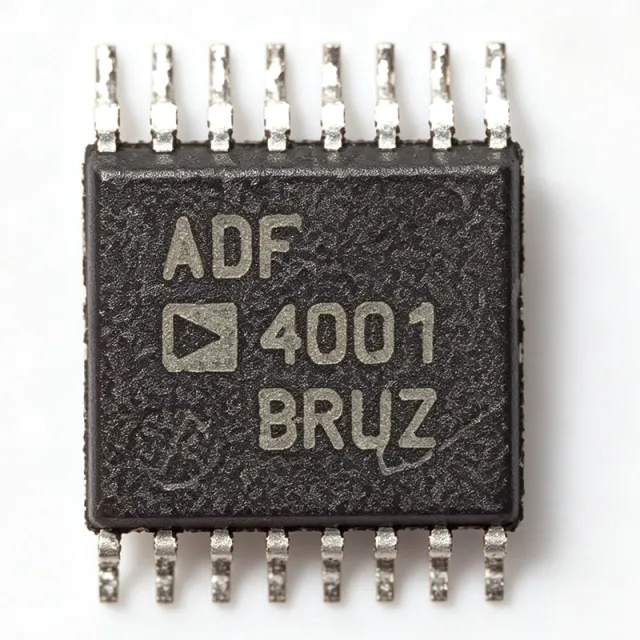
AD4001BRUZ - 16-Bit 2MSPS Differential SAR ADC | Analog Devices
The AD4001BRUZ is a 16-bit, 2 MSPS precision successive approximation register (SAR) analog-to-digital converter (ADC) from Analog Devices. It features a fully differential input, a high-speed serial interface, and operates from a single 1.8 V supply. The device is available in a 16-lead TSSOP package, making it suitable for space-constrained precision data acquisition systems. An ADC (analog-to-digital converter) is an electronic component that converts continuous analog signals into discrete digital values. The AD4001BRUZ is a SAR ADC, which uses a binary search algorithm to determine the digital output. SAR ADCs are known for their high speed, low power, and excellent accuracy, making them ideal for applications such as industrial process control, medical instrumentation, and test and measurement equipment. The AD4001BRUZ is part of the precision ADC family, which includes other high-performance converters from Analog Devices. Key features of the AD4001BRUZ include a 2 MSPS throughput, 16-bit resolution, and a differential input range that can be configured via the reference voltage. The device offers a high signal-to-noise ratio (SNR) and low power consumption, typically 15 mW at 2 MSPS. It also includes an input overvoltage clamp that protects the ADC inputs from overvoltage events, minimizing disturbances on the reference pin and eliminating the need for external protection diodes. The serial interface is SPI-compatible and supports daisy-chaining for multiple ADCs. The AD4001BRUZ uses a precision capacitive DAC architecture with a track-and-hold circuit, ensuring accurate conversion of fast-changing signals. The device operates from a 1.8 V analog supply and a separate digital supply, allowing flexible interfacing with different logic levels. The reference input accepts a wide range of voltages, enabling the user to scale the input span to match the application requirements. The device also features a busy indicator and a conversion result readback that can be synchronized with an external clock. Typical applications for the AD4001BRUZ include industrial automation, data acquisition systems, medical imaging, and portable instrumentation. Its high speed and precision make it suitable for applications that require accurate measurement of dynamic signals, such as vibration analysis and motor control. The small TSSOP package and low power consumption make it ideal for battery-powered devices. When designing with the AD4001BRUZ, it is important to provide a clean, low-noise reference voltage and adequate decoupling on the power supply pins. The input signal should be driven by a low-impedance source, such as an operational amplifier, to ensure accurate conversion. The SPI interface should be configured for the correct clock polarity and phase to match the device's timing requirements.

AD4002BRUZ - 18-Bit SAR ADC, 2 MSPS | Analog Devices
The AD4002BRUZ is a high accuracy, high speed, low power, 18-bit, Easy Drive, precision successive approximation register (SAR) analog-to-digital converter (ADC) from Analog Devices. It operates from a single power supply, VDD, and features a reference voltage, VREF, that sets the input range. The device is available in a 16-lead TSSOP package, making it suitable for space-constrained applications. A SAR ADC is a type of analog-to-digital converter that uses a successive approximation register to convert an analog input signal into a digital output. It works by comparing the input voltage against a series of binary-weighted reference voltages, refining the approximation with each clock cycle. SAR ADCs are known for their high speed, low power consumption, and ease of use, making them ideal for applications such as data acquisition, industrial process control, and medical instrumentation. Key features of the AD4002BRUZ include 18-bit resolution, a maximum sampling rate of 2 MSPS, and an Easy Drive architecture that simplifies the analog front-end design by reducing input drive requirements. The device also features input span compression, which eliminates the need for a negative supply to the ADC driver amplifier while preserving access to the full ADC code range. An input overvoltage clamp protects the ADC inputs against overvoltage events, minimizing disturbances on the reference pin and eliminating the need for external protection diodes. Technically, the AD4002BRUZ uses a precision SAR architecture with an internal reference buffer, ensuring high linearity and low noise. The device supports a wide input voltage range and operates from a single 1.8V to 5V supply, making it versatile for various system power rails. The Easy Drive feature reduces the settling time requirements of the driving amplifier, allowing for lower power and simpler front-end designs. Typical applications include high-speed data acquisition systems, industrial automation, medical imaging, and precision instrumentation. The AD4002BRUZ is also suitable for battery-powered devices due to its low power consumption. When designing with this ADC, ensure proper decoupling of the VDD and VREF pins and consider the input overvoltage clamp for robust operation in harsh environments.