دوائر المضخم المتكاملة
المنتجات (1,100+)

LM324QDRQ1 - Automotive Quad Op Amp, 1MHz, RRO | TI
The Texas Instruments LM324QDRQ1 is an automotive-qualified quad operational amplifier delivering a 1 MHz gain-bandwidth product and rail-to-rail output (RRO) swing in a 14-pin SOIC (D) surface-mount package. It operates from a single supply of 2.7 V to 5.5 V (or dual supplies of +/-1.35 V to +/-2.75 V), making it well suited to battery-powered and low-voltage automotive systems. An operational amplifier (op amp) is a high-gain differential-input voltage amplifier and one of the most fundamental building blocks in analog electronics, used for signal conditioning, active filtering, and mathematical operations. Within the analog IC hierarchy, general-purpose op amps belong to linear integrated circuits, alongside comparators, voltage references, and voltage regulators. Quad op amps like this device integrate four matched amplifiers on a single die, saving board space and improving channel matching in multi-channel signal chains. Key features include rail-to-rail output swing that maximizes dynamic range at low supply voltages, a maximum input offset voltage of 4 mV, and a typical common-mode rejection ratio (CMRR) of 65 dB. Each amplifier draws approximately 100 uA of quiescent current, enabling low-power designs, while internal frequency compensation guarantees unity-gain stability without external components. Technically, the device uses bipolar process technology for good linearity, includes short-circuit protection and output current limiting for robustness, and specifies output current capability of around 160 mA per channel under rated conditions per distributor data. The AEC-Q100 qualification and wide temperature rating make it suitable for harsh automotive environments with 3.3 V and 5 V microcontroller-based systems. Typical applications include automotive sensor signal conditioning (temperature, pressure, and position sensors), battery management system monitoring front-ends, and motor control circuits paired with MCUs such as TI C2000 and MSPM0 families. Design tip: decouple the supply pin with a 0.1 uF ceramic capacitor placed close to the device, and respect the input common-mode range, which extends from ground to VCC - 1.5 V, to avoid phase-reversal and nonlinear behavior near the upper rail.

LM324QT - Quad Low Power Op Amp, 1.3MHz | STMicroelectronics
The LM324QT from STMicroelectronics is a quad general-purpose operational amplifier in a compact 16-pin QFN (3x3 mm) package. It operates from a single power supply over a wide voltage range, making it ideal for space-constrained, battery-powered applications. The device features four independent, high-gain, frequency-compensated amplifiers with a gain bandwidth product of 1.3 MHz and a slew rate of 0.4 V/us. An operational amplifier (op amp) is a high-gain voltage amplifier with differential inputs and a single-ended output. It is the fundamental building block of analog signal conditioning, used in filters, comparators, integrators, and many other circuits. The LM324QT belongs to the LM324 family, a classic industry-standard quad op amp known for its low power consumption and wide supply range, which includes the ability to operate from a single supply down to 3V. Key features include a wide gain bandwidth of 1.3 MHz, a large voltage gain of 100 dB, and a very low supply current per amplifier of 375 uA. The input common-mode voltage range includes ground, allowing single-supply operation with ground-referenced inputs. The device also features low input bias current and internal frequency compensation, simplifying design and reducing external component count. The LM324QT uses a bipolar process technology, providing robust performance over a wide temperature range. The QFN package offers excellent thermal performance and a small footprint, making it suitable for compact designs. The device is designed for low-power operation, making it ideal for battery-powered equipment where power efficiency is critical. Typical applications include sensor signal conditioning, active filters, DC gain blocks, and transducer amplifiers. The wide supply voltage range and low power consumption make it suitable for automotive, industrial, and consumer electronics. The QFN package is particularly well-suited for portable devices where board space is at a premium. When designing with the LM324QT, ensure proper decoupling of the power supply pins with a 0.1 uF ceramic capacitor placed close to the device. The input common-mode range includes ground, but for best performance, keep inputs within the specified range. The output can swing close to the rails, but avoid driving loads that require rail-to-rail output swing without proper design considerations.

LM339AM - Quad Open-Collector Comparator | Texas Instruments
The Texas Instruments LM339AM is a low-power, low-offset, quad differential voltage comparator with four independent comparison channels, an open-collector output stage, and a 14-pin SOIC package. The device supports input voltages spanning ground in the common-mode range, a differential input rating up to 38 V, and compatibility with DTL, MOS, TTL, and CMOS logic families. Its specified operating-temperature range for this ordering code is 0°C to 70°C. A comparator is an analog integrated circuit that compares two input voltages and changes its output state when the non-inverting input rises above the inverting input. The LM339 belongs to the voltage-comparator hierarchy, which falls within analog and mixed-signal ICs and ultimately the broader semiconductor category. Its four channels can operate independently or be configured as two window or hysteretic comparison functions. Key features include four open-collector outputs, low quiescent current, low input offset voltage, and wide input-voltage capability. The open-collector architecture requires an external pull-up resistor and permits several open-collector outputs to share a wired bus when their device-current limits and logic levels are compatible. The 14-pin SOIC package supports conventional surface-mount assembly while providing separate inputs, outputs, and two ground pins. Internally, each channel uses a differential input stage followed by an open-collector output stage. The inputs can be driven near ground, making the device suitable for low-level sensing where the signal of interest lies close to the lower supply rail. Because the outputs are open collectors rather than push-pull outputs, output rise time depends on the pull-up resistor, bus capacitance, and leakage current rather than only on the comparator itself. Typical applications include battery threshold detection, sensor-level conditioning, window comparators, industrial control interfaces, and low-level memory or control monitoring. Industrial systems benefit from the wide common-mode capability, while consumer and communication equipment can use the open-collector outputs directly with pull-up resistors. Four independent channels also reduce the component count in multi-level or multi-signal designs. Designers should verify supply voltage, input common-mode limits, output pull-up values, and propagation delay under the intended load. The open-collector output must never be left without a pull-up path, and unused comparator inputs should be tied to a defined potential to prevent unintended switching. PCB placement should keep pull-up resistors close to the output pins and minimize routing through noisy analog or switching nodes. This page combines the supplied manufacturer and distributor information with practical pin, replacement, application, and design guidance. It also distinguishes verified ordering information from details that must still be confirmed against the manufacturer datasheet before production release.

LM339AN - Quad Open-Collector Comparator | Texas Instruments
The Texas Instruments LM339AN is a four-channel general-purpose differential voltage comparator with an open-collector output, a 2 V to 36 V supply range, and a 14-pin PDIP package. Each channel supports single-supply or split-supply operation, while the 1.3 µs response time suits general detection and threshold-control applications. The LM339A family provides a maximum input offset voltage of 2 mV and can operate with input voltages extending to ground on the negative supply. A voltage comparator is an analog integrated circuit that compares two input voltages and produces a logic-level output indicating which input is higher. The LM339AN belongs to the comparator family within analog and amplifier ICs, which sits within the broader integrated-circuit and semiconductor hierarchy. Its four independent channels allow multiple sensing, protection, or control functions to share one package without requiring four separate comparator devices. Key features include four independent comparators, open-collector outputs, 2 V to 36 V operating supply voltage, ±1 V to ±18 V differential input capability, and a 1.3 µs response time. The open-collector architecture provides flexible output interfacing because each output can pull a logic rail low through an external pull-up resistor. This arrangement works with TTL, CMOS, and MOS-compatible logic, although it adds a pull-up component and can expose the output node to more noise when the resistor is weak. The LM339AN uses a low-power bipolar comparator architecture optimized for general-purpose level detection rather than high-speed precision instrumentation. Its common-mode input range includes ground, making it useful in single 5 V or single 12 V systems where a signal approaches zero volts. The 2 mV maximum offset specification for the LM339A family helps limit transition-point error, while the 1.3 µs response time provides useful speed for relay, lamp, and simple control-loop decisions. Typical applications include sensor threshold detection, overvoltage and undervoltage protection, battery monitoring, industrial control inputs, window or level comparators, and general logic interfacing. Four channels can monitor four related signals independently, making the device suitable for multi-parameter protection boards and compact industrial interface modules. The open-collector outputs can drive a relay driver, an optocoupler, a status LED, or a logic input when an appropriate pull-up resistor is installed. Designers should treat all unused input pins carefully, provide adequate input-common-mode headroom, and select a pull-up resistor that balances speed, power, and noise performance. Because the outputs are open collector, multiple LM339AN channels may share a common pull-up node when their wired-OR behavior is acceptable. PCB creepage, grounding, and the relationship between the measured signal and the comparator threshold are equally important for reliable industrial operation. This page combines the verified manufacturer and distributor information for the LM339AN with package-specific pin mapping, transparent sourcing, and practical design guidance. It also distinguishes direct same-package alternatives from the broader LM339 family, helping engineers evaluate replacement options without confusing electrical equivalence with guaranteed mechanical or temperature-grade equivalence.
LM339D - 4-Comparator Open-Collector IC | Texas Instruments
The Texas Instruments LM339D is a general-purpose quad differential voltage comparator containing four independent comparator channels, open-collector outputs, and operation from a single positive supply in a 14-pin SOIC package. The verified manufacturer data identifies a maximum rating up to 38 V, input offset voltage of 0.37 mV, input bias current of 3.5 nA, supply current of 200 µA per comparator, and response time of 1 µsec for the related LM339 family. These values make the device suitable for level detection, low-level sensing, memory applications, and general industrial threshold circuits. A voltage comparator is an analog comparator that evaluates two input voltages and changes its output state according to their relationship. The LM339 belongs to the comparator, analog IC, and signal-conditioning hierarchy. Unlike an op-amp configured for linear amplification, a comparator is intended for open-loop decision making. Its open-collector output requires an external pull-up resistor and can be wired with multiple comparator outputs when the electrical conditions permit. The four independent channels allow one package to perform several threshold decisions. Open-collector outputs can interface with TTL, MOS, and CMOS-compatible circuits according to the family documentation, while the wide supply capability supports industrial and automotive-style environments. The low input bias current is useful when the comparator senses high-impedance sources, although input offset, common-mode range, output saturation, and supply limits must still be checked in the complete design. The LM339 family is supported by TI’s application guidance for TL331, LM339, and LM393 devices, which emphasizes correct use of open-collector outputs, pull-up networks, input protection, and supply bypassing. The package and pin arrangement should be verified against the selected manufacturer’s datasheet before layout release, especially when replacing a part sourced from another manufacturer. Typical applications include sensor threshold detection, battery or power-system monitoring, window comparator circuits, logic-level translation, relay or solenoid drive interfaces, and industrial control inputs. An external pull-up resistor is normally placed from each output to the downstream logic supply so that the open-collector transistor can pull the line low and release it high. The main design consideration is that an open-collector output is not a push-pull logic output. Choose the pull-up voltage and resistor for the receiving device, verify output sink current, and account for the positive logic level at the receiver input. Place bypass capacitors close to the supply pins and keep sensitive input traces away from output and switching-current paths. This product page consolidates verified distributor identity, manufacturer family specifications, package information, sourcing links, and engineering-oriented usage guidance. Exact pricing, stock, alternative parameter tables, and manufacturer-specific pin details remain dependent on the cited source pages and are not inferred where the supplied evidence is incomplete.
LM339DR - Quad Differential Comparator, Open-Collector | TI
The Texas Instruments LM339DR is a quad differential comparator that integrates four independent precision voltage comparators into a single 14-pin SOIC package. The device operates from a single power supply over a wide voltage range and is well-suited for use in voltage-level detection, threshold detection, and analog signal conditioning circuits. The LM339DR outputs are open-collector and require a pull-up resistor to a supply ranging from 5V to 36V (or higher), enabling level-shifting between incompatible logic domains. What is an analog comparator? An analog comparator is an active circuit element that compares two input voltages and produces a binary output based on which is larger. Comparators sit alongside op-amps and ADCs in the signal-chain hierarchy: op-amp (linear amplification) -> comparator (1-bit decision) -> Schmitt trigger (hysteresis-based decision). The LM339 family sits in the general-purpose comparator category, optimized for cost and versatility rather than speed or precision. Key features of the LM339DR include a typical input offset voltage of 2 mV, a wide common-mode input voltage range that includes ground, a differential input voltage range equal to the maximum-rated supply voltage, and an operating supply range of 2V to 36V. The device draws a low supply current of approximately 1 mA (200 uA per comparator in the newer LM339B), and outputs are compatible with TTL, MOS, and CMOS logic families. Operating temperature range spans 0C to +70C in the standard commercial grade, with automotive-grade LM2901 variants covering -40C to +125C. The LM339DR architecture uses a bipolar transistor design with Darlington NPN output stages driving open-collector transistors. This architecture provides high input impedance and stable switching thresholds, though response time is in the microsecond range rather than the nanosecond range of high-speed comparators. The device is internally compensated and requires no external frequency-compensation components. Typical applications include overvoltage/undervoltage protection circuits, zero-crossing detectors, oscillator circuits, window comparators, and sensor-signal level translation. Industrial uses include battery chargers, switch-mode power supply feedback loops, and motor-control interface circuits. Designers should note that open-collector outputs require external pull-up resistors and that output transition time is dominated by the RC time constant of the pull-up resistor and load capacitance. For high-speed applications, choose a comparator with push-pull outputs such as the TL331 family. This page synthesizes distributor pricing, drop-in alternatives, and practical design notes not found in the standalone TI datasheet, providing engineers a single-point comparison resource.
LM339M - Quad Open-Collector Comparator | Texas Instruments
The Texas Instruments LM339M is a low-power, low-offset-voltage quad comparator containing four independent voltage comparators in a 14-pin SOIC package. It supports single or dual supplies, operates from 2 V to 36 V, accepts input voltages up to ±18 V relative to the supply arrangement, and provides open-collector outputs. The verified data identifies a response time of 1.3 µs, typical supply current drain of 800 µA, and typical input bias current of 25 nA. A comparator is an analog integrated circuit that compares two input voltages and produces a digital logic state indicating which input is higher. The LM339 belongs to the broader hierarchy of analog comparator ICs, voltage-detection devices, and general-purpose signal-conditioning components. Its four independent channels allow one package to implement multiple threshold, overvoltage, undervoltage, window, or sorting decisions while sharing a common supply architecture. Key features include four open-collector outputs, low supply current, low input bias current, low-offset operation, and an input common-mode range that includes ground on single-supply systems. Open-collector outputs require an external pull-up resistor and can support wired logic, connector interfaces, level translation, or multiple devices sharing a bus when the electrical conditions are appropriate. Unlike a push-pull output, this architecture provides useful flexibility at the cost of requiring an external pull-up and having a slower rising edge. The LM339M can operate from 2 V to 36 V, while the verified distributor listing identifies SOIC-14 packaging and a 0 °C to 70 °C temperature grade for the listed Texas Instruments LM339M variant. The four comparators share supply pins but have independent noninverting and inverting inputs. Pin assignment and input polarity must be verified against the manufacturer datasheet before layout, especially because the M suffix identifies the package configuration rather than a different comparator function. Typical applications include DC overvoltage and undervoltage detection, battery threshold monitoring, industrial control interfaces, sensor conditioning, open-collector alarm signaling, and four-channel comparator banks in embedded systems. A pull-up resistor on each output is normally required. Inputs must remain within the device’s common-mode limits, and supply bypass should follow the manufacturer’s recommended layout practice to reduce susceptibility to switching noise and lead instability. This page consolidates the verified LM339M specifications, source links, packaging information, and application-oriented design guidance. It deliberately separates confirmed values from unspecified electrical details; parameters not present in the supplied data are not inferred here.
LM339MX - Quad Open-Collector Comparator | Texas Instruments
The Texas Instruments LM339MX is a general-purpose quad voltage comparator containing four independent comparator channels in a 14-pin SOIC package. Each channel supports single or dual power-supply operation across a total range of approximately 36 V, or approximately ±18 V, and uses an open-collector output. Verified distributor data identifies a response time of 1.3 µs, output compatibility with TTL, CMOS, MOS, DTL, and ECL logic, and an operating temperature range of 0 °C to 70 °C. A voltage comparator is an analog signal-conditioning integrated circuit that compares two input voltages and changes its output state when the non-inverting input exceeds the inverting input. The comparator category belongs to the wider hierarchy of analog IC, signal-conditioning IC, logic-interface IC, and semiconductor. The LM339MX is therefore positioned between precision analog conversion and digital logic systems, converting a small voltage difference into a logic-level transition that can drive digital control, protection, or monitoring circuitry. The four independent channels make the LM339MX suitable for multi-threshold monitoring without requiring four separate packages. Its open-collector outputs permit wired-AND behavior when multiple channels or external devices pull the same output node low. Each channel also supports a pull-up arrangement rather than driving the output rail directly, allowing interface compatibility with different logic families. The approximately 1.3 µs response time makes the device suitable for general-purpose control loops rather than high-speed edge-detection applications. The 14-pin SOIC footprint supports compact through-hole-style PCB assembly and is pin-compatible with common LM339-family and general-purpose quad-comparator implementations. Because the outputs are open collector, a pull-up resistor is normally required when driving CMOS or TTL inputs. The four channels share supply and ground pins, so decoupling should be placed close to the package power pins and the ground return should follow a low-impedance path. Typical uses include overvoltage and undervoltage monitoring, power-supply sequencing, battery threshold detection, window comparators, motor-control interfaces, and industrial control systems. Compared with faster rail-to-rail comparators, the LM339MX emphasizes wide supply operation, multiple logic-output compatibility, and a straightforward open-collector interface rather than low-power or nanopower operation. For new designs, verify the exact input common-mode range, output-current limits, and switching behavior against the selected manufacturer datasheet because these values were not included in the retrieved source snippets. This page combines verified distributor specifications, package details, drop-in alternatives, and application guidance to support engineering selection.
LM339N - Quad Open-Collector Comparator | Texas Instruments
The Texas Instruments LM339N is a low-power, low-offset quad differential comparator containing four independent comparator channels in a 14-pin PDIP package. The verified source identifies the device as a general-purpose comparator with open-collector outputs, a 2 V to 36 V supply range, and approximately 1.3 microsecond response time. Each channel can compare two input voltages, while its open-collector output requires an external pull-up resistor for a usable logic-high level. A quad comparator is an analog comparator integrated circuit used to determine whether an input voltage is higher or lower than a reference voltage. The comparator function belongs to the broader analog and mixed-signal semiconductor hierarchy: comparator -> differential comparator -> analog IC -> semiconductor. LM339N provides four channels in one package, reducing component count when a system needs several independent threshold, sorting, overvoltage, or sensing decisions. The main verified characteristics are four independent comparator sections, open-collector outputs, a 14-pin PDIP package, and a wide operating supply range of 2 V to 36 V. The manufacturer describes the LM339-N family as a low-power, low-offset voltage quad comparator. Because the outputs are open collector, the output stage can sink current but does not actively drive a high voltage; an external resistor connects the output node to the desired positive supply. This arrangement supports wired logic, relay or lamp drive, and level translation when the pull-up voltage is selected appropriately. The open-collector architecture also provides a useful benefit in multi-comparator systems: several outputs can be connected to a common pull-up node when the application intentionally requires wired-AND behavior. The design must account for the voltage and current limits of every connected output and for the sink-current capability of each comparator. The external pull-up resistor also affects rise time, so a lower resistance can improve speed while increasing current and power dissipation. Typical uses include DC threshold detection, battery and supply monitoring, window comparison, industrial control logic, sensor conditioning, overvoltage indication, and general-purpose analog decision circuits. The four channels can be used for independent comparisons or arranged as a multi-level voltage detector. Because input and output details beyond the verified source were not supplied, exact input common-mode limits, output sink-current limits, input offset, response-time conditions, and temperature ranges should be confirmed in the manufacturer datasheet before production release. The LM339N is primarily a through-hole general-purpose comparator rather than a high-speed logic device. Its strength is simple wide-supply operation with four channels and open-collector outputs. A PCB design should route comparator inputs away from switching nodes, provide a stable reference, use a defined ground return, and choose pull-up resistors according to the required logic voltage, rise time, and current budget. This page combines verified distributor and manufacturer information with application-oriented design guidance while avoiding unsupported numeric claims.
LM339NG - 3-36V Quad Open-Collector Comparator | onsemi
The onsemi LM339NG is a four-channel general-purpose analog comparator with a 3 V to 36 V single-supply operating range, open-collector CMOS/TTL-compatible outputs, and a 14-pin PDIP package. Each channel compares two input voltages, making the device suitable for level detection, low-level sensing, memory applications, threshold control, and industrial interface circuits. The LM339NG supports single or split supply operation. An analog comparator is an integrated circuit that determines whether an input voltage is above or below a reference voltage. In the broader electronics hierarchy, a comparator belongs to the analog IC and signal-conditioning category, where it converts a continuously varying voltage relationship into a logic-level decision. Unlike an operational amplifier, a comparator is optimized for fast switching between output states rather than linear amplification. The four independent LM339NG channels combine a wide supply-voltage range with low input bias current. Verified sources report a typical input bias current of 25 nA, a typical input offset current of ±5 nA, and an input offset voltage of 1.3 mV. The distributor descriptions identify the outputs as open collector, allowing the output stage to sink current rather than actively sourcing it. This architecture requires an external pull-up resistor when the comparator must produce a valid high level. With a response time of approximately 1.3 microseconds, the LM339NG is suitable for general-purpose detection rather than very high-speed signal comparison. Its 14-pin PDIP construction supports through-hole assembly and is useful in industrial control equipment, automotive electronic modules, consumer appliances, memory-control circuits, and laboratory interface boards. The package is also readily inspected or replaced during maintenance. A key design consideration is the open-collector output. Each output requires a pull-up resistor to the appropriate logic supply, and the pull-up voltage must not exceed the applicable device limits. Input common-mode range, output saturation, input protection, and supply-current behavior should be checked against the manufacturer datasheet before operation near the supply extremes. This page consolidates verified distributor information, source-linked specifications, practical application guidance, and cautious drop-in alternatives. It also distinguishes confirmed LM339NG characteristics from attributes that still require full datasheet or application-specific verification before production use.

LM339PT - 4-Channel Open-Collector Comparator | STMicroelectronics
The STMicroelectronics LM339PT is a low-power quad voltage comparator containing four independent comparison channels in a 14-pin TSSOP package. Each channel supports single-supply or split-supply operation and uses an open-collector output, allowing the outputs to be wired together for wired-AND behavior. The verified product data identifies a 1 V to 16 V supply range, a maximum input offset voltage of 2 mV for the A-grade device family, and compatibility with CMOS, DTL, ECL, MOS, open-collector, and TTL logic. A voltage comparator is an analog integrated circuit that compares two input voltages and changes its output state according to their relationship. The LM339 belongs to the comparator hierarchy within analog and mixed-signal semiconductors. Its four independent channels can perform threshold detection, overvoltage monitoring, window comparison, zero-crossing detection, and general-purpose signal conditioning. Unlike a digital logic gate, the comparator evaluates continuously varying analog voltages at its inputs. The main feature of the LM339PT is its combination of four independent open-collector comparators in one compact TSSOP-14 package. Its low-power design is suitable for battery-powered equipment, while the broad supply-voltage range supports industrial control and instrumentation systems. The open-collector architecture requires an external pull-up resistor and can interface with CMOS or TTL logic. The verified distributor description also reports a propagation delay of 1.3 µs, making the device suitable for moderate-speed threshold and protection functions rather than ultra-high-speed applications. Each comparator channel has two input pins, an output, and access to the device ground and supply pins. The outputs are open-collector rather than push-pull, so an output can sink current while remaining high-impedance when inactive. Pull-up resistors are therefore required on every used output. Connecting outputs together requires compatible pull-up arrangements and careful review of the maximum sink-current and voltage limits. The device does not provide a latch function, so applications requiring state retention normally add external feedback or latch circuitry. Typical uses include DC overvoltage detection, power-supply sequencing, sensor threshold switching, battery monitoring, industrial control interfaces, and logic-level conversion. Split-supply operation allows the comparator to evaluate signals around ground, while single-supply operation is useful when all measured signals remain above the common-mode limits. Because the outputs are open collector, the device can also connect to buses such as SMBus or I2C where wired-AND behavior is required, provided the electrical and timing requirements of the specific bus are satisfied. Designers should account for input common-mode range, output pull-up resistance, supply decoupling, and the behavior of the open-collector output at temperature extremes. Place the device close to the protected signal and provide a stable ground reference. Avoid relying on an output to source current, and select a pull-up voltage compatible with both the comparator output ratings and the driven logic family. The TSSOP-14 package supports compact PCB layouts, but pin-1 orientation must be checked carefully because closely spaced leads can complicate hand rework. This product page consolidates verified distributor availability and pricing, package information, same-package cross-references, and practical design guidance. It also distinguishes drop-in replacements from devices that differ in package or temperature grade, helping engineers make a replacement decision without assuming that every similarly named LM339 variant is electrically and mechanically interchangeable.

LM358AD - Dual Low Power Op-Amp, 1.1MHz, SOIC-8 | STMicroelectronics
The STMicroelectronics LM358AD is a low-power dual operational amplifier consisting of two independent, high-gain, internally frequency-compensated op-amps designed to operate from a single power supply across a wide voltage range. Housed in an 8-pin SOIC package, the LM358AD delivers a unity-gain bandwidth of approximately 1.1 MHz, a slew rate of 0.6 V/µs, and supports supply voltages from 3V to 30V single-supply or ±1.5V to ±16V dual-supply. The device is widely used in cost-sensitive analog front-ends where single-supply operation and low quiescent current are essential design constraints. An operational amplifier (op-amp) is a high-gain, DC-coupled electronic voltage amplifier with differential inputs and a single-ended output. Within the broader power management and signal conditioning hierarchy, the LM358AD belongs to the general-purpose op-amp category, sitting between precision instrumentation amplifiers (high accuracy, low noise) and high-speed amplifiers (wide bandwidth, fast slew). Op-amps form the building blocks of analog signal chains: filters, comparators, integrators, transducers, sensor signal conditioners, and active rectifiers. The LM358 family specifically targets single-supply 5V/12V/24V systems that cannot tolerate the negative rail required by legacy op-amps like the LM741. Key features include: 1.1 MHz gain-bandwidth product, 0.6 V/µs slew rate, input common-mode range that includes ground (enabling true single-supply sensing near 0V), low input bias current, internal frequency compensation (no external capacitor required), and ESD protection on the inputs. The output stage can swing to within a few hundred millivolts of the negative rail, although it does not reach the positive rail — meaning the part is not rail-to-rail but is sufficient for most single-supply transducer interfaces. Technically, the LM358AD uses a bipolar junction transistor (BJT) input stage rather than JFET or CMOS, which trades higher input bias current (~45 nA typical) for extremely low input offset voltage drift and predictable behavior across temperature. The two amplifiers share only the power pins; their inputs and outputs are fully independent, allowing asymmetric configurations such as one channel as a comparator and the other as a gain stage. Typical applications include battery-powered sensor signal conditioning, transducer amplifiers, DC gain blocks, active filters, integrators, comparators with hysteresis, and 4–20 mA current loop transmitters. Industrial designs frequently use the LM358AD in 24V PLC analog input modules, while consumer designs use it for white-goods sensor interfaces and IoT battery nodes. When designing with this device, remember that the output cannot swing to the positive rail — typically VOH stops around VCC−1.5V at 10 mA load. Place a 100 nF bypass capacitor close to VCC and ground, and use a feedback resistor of at least 10 kΩ to limit output stage loading. This page synthesizes distributor pricing, drop-in alternatives, and practical design notes not found in the manufacturer datasheet.

LM358ADDR - Dual 30V 700kHz Op Amp | Texas Instruments
The LM358ADDR is a dual operational amplifier from Texas Instruments, part of the industry-standard LM358 family. It operates from a single supply of 3V to 30V or dual supplies of +/-1.5V to +/-15V, with a typical supply current of 500uA per amplifier, packaged in an 8-pin SOIC (D) surface-mount package delivered in tape and reel. An operational amplifier (op amp) is a high-gain voltage amplifier with differential inputs and a single-ended output. It is a fundamental building block of analog electronics used in signal conditioning, filtering, and mathematical operations. The LM358 is a dual op amp containing two independent amplifiers in one package, offering design flexibility and space savings. It belongs to the broader category of linear integrated circuits (amplifier ICs) used across power management, sensor interfaces, and audio processing. Key features include a common-mode input voltage range that extends to ground, enabling true single-supply operation with inputs referenced to ground. The gain-bandwidth product is 700kHz with a 0.3V/us slew rate, and maximum input offset voltage is 3mV. The operating temperature range is 0C to 70C for commercial applications. The device is RoHS compliant and lead-free. Technically, the LM358 uses a bipolar process with a class-AB output stage for low output distortion. The PNP input pair enables the input common-mode range to include ground. The output swings close to but not rail-to-rail, a consideration for maximum-swing designs. Internal frequency compensation ensures unity-gain stability without external components. Typical applications include transducer amplifiers, DC gain blocks, active filters, battery chargers, power supply control, and motor control loops. The dual configuration handles multiple signal paths in a compact footprint, reducing board space and component count. When designing with the LM358ADDR, ensure input voltage does not exceed the supply rails to avoid phase reversal, decouple supply pins with 0.1uF capacitors, and account for output swing typically 1.5V from the rails. Pricing as of 2026-08-29 starts near $0.0541 at LCSC.
LM358AM - Dual 8-SOIC Operational Amplifier | Texas Instruments
The Texas Instruments LM358AM is a dual general-purpose operational amplifier with two independent, internally frequency-compensated amplifier channels in an 8-pin SOIC package. The device is designed for operation from a single power supply over a wide voltage range, providing a practical solution where two amplified signals must be processed by one compact analog IC. The verified product information identifies the LM358AM as a standard, general-purpose, two-circuit amplifier and describes its low-power consumption, high gain, and wide operating-voltage capability. An operational amplifier, or op-amp, is a voltage-controlled differential amplifier whose closed-loop behavior is determined mainly by external feedback components. The LM358 belongs to the broad hierarchy of operational amplifiers, analog amplifiers, analog signal-conditioning ICs, and semiconductor devices. Its two internally compensated channels can perform common tasks such as voltage amplification, buffering, summing, comparisons, active filtering, and feedback control when configured with suitable external resistors and capacitors. The principal advantages of choosing a dual amplifier are functional integration and reduced board area. Two independent amplifiers in one LM358AM package can replace two separate single-channel devices while preserving the familiar SOIC-8 footprint. The manufacturer describes the series as suitable for general-purpose applications and emphasizes its combination of low power consumption, high gain, and a wide supply-voltage range. Exact voltage, current, gain-bandwidth, input-offset, and temperature limits require confirmation from the full manufacturer datasheet because those values were not included in the supplied web records. The architecture is based on two independent, high-gain, internally frequency-compensated operational amplifiers. Internal frequency compensation avoids the need for an external compensation capacitor in ordinary closed-loop configurations, simplifying amplifier selection and PCB design. Because the channels are independent, one can amplify a sensor signal while the other performs a different function, such as comparison, current-to-voltage conversion, active filtering, or an output driver. Typical uses include industrial sensor conditioning, low-cost control loops, audio preamplification, current sensing, comparator-style threshold detection, and general analog signal processing. Single-supply operation is particularly useful in embedded equipment because the amplifier can operate from a positive rail and ground. Designers must still check input and output common-mode limits, output-swing behavior, load capability, and stability for the intended configuration before releasing production hardware. PCB implementation should preserve the exact pin assignment of the chosen SOIC-8 manufacturer variant and provide a solid ground return. Decoupling capacitors should be placed close to the supply pins, while feedback resistors and compensation networks should be kept short to minimize noise pickup and parasitic instability. The LM358AM is not rail-to-rail by implication alone; input and output behavior must be verified against the relevant datasheet limits. This product record combines verified distributor and manufacturer references, package information, commercial availability links, and practical selection guidance. It also separates documented facts from missing numeric parameters so engineers can cross-check voltage limits, pricing, compliance, and production details against the authoritative LM358 datasheet before design release.
LM358D - Dual 700kHz General Purpose Op Amp | Texas Instruments (Tape & Reel)
The LM358D is a dual operational amplifier from Texas Instruments in an 8-pin SOIC (D) surface-mount package. It operates from a single supply of 3V to 32V or dual supplies of ±1.5V to ±16V, with a gain bandwidth product of 700 kHz and a slew rate of 0.3 V/µs. This industry-standard, low-cost amplifier serves a vast range of general-purpose analog functions. An operational amplifier (op amp) is a high-gain differential-input, single-ended-output voltage amplifier and one of the most fundamental building blocks in analog electronics. General-purpose op amps like the LM358 prioritize versatility, low cost, and ease of use over precision or bandwidth. The LM358 is the dual version of the LM321 single amplifier and the two-amp counterpart of the quad LM324. Key features include a common-mode input voltage range that extends to ground, enabling direct sensing near ground in single-supply systems; low supply current of 0.7 mA typ, independent of supply voltage; internal frequency compensation for unity-gain stability; and short-circuit protected outputs. These characteristics suit battery-powered and cost-sensitive designs. Technically, the LM358 uses a bipolar process with a class-AB output stage that can drive loads as low as 2 kΩ with a large output swing. The commercial temperature grade is 0°C to +70°C. Input bias and offset currents are low, and the two internal amplifiers are well matched, sharing the same supply and bias circuitry. Typical applications include transducer amplifier front ends, DC gain blocks, active RC filters, voltage comparators and level shifters, power-supply feedback loops, and portable or industrial control electronics. The SOIC-8 package supports automated SMT assembly and reflow. Design considerations: decouple V+ to GND with a 0.1 µF ceramic capacitor close to pin 8, and respect output swing limits near the rails (output saturates roughly 1.5V below V+ at moderate loads). For higher bandwidth or lower noise, consider the pin-compatible TLV9152 or TL072. Pricing as of 2026-08-30 starts around $0.05 at volume from distributors such as LCSC.
LM358DG - Dual 1 MHz Operational Amplifier | onsemi
The onsemi LM358DG is a dual general-purpose operational amplifier with two amplifier channels, 1 MHz gain-bandwidth product, 0.6 V/µs slew rate, and a 3 V to 32 V operating supply range. The device is supplied in an 8-SOIC package and supports both single-supply and split-supply operation. Its common-mode input range extends to ground and VEE, making it suitable for signal conditioning, current monitoring, and general industrial-control circuits. An operational amplifier is an analog integrated circuit that uses high-gain differential amplification and feedback to control gain accurately. The dual LM358 architecture provides two amplifiers in one package, reducing board area while offering independent input, output, and supply connections. The LM358 belongs to the operational-amplifier hierarchy, which also includes single and quad amplifier packages used in instrumentation, sensor interfaces, and power-management systems. Key characteristics include a 3 V to 32 V supply range, 1 MHz gain-bandwidth product, 0.6 V/µs slew rate, and a common-mode rejection ratio listed at a minimum of 65 dB. Input offset voltage is listed as 7 mV. The common-mode input voltage range extends to ground or VEE, allowing the amplifier to process signals near the lower supply rail. Low power drain and single- or split-supply flexibility suit both portable and industrial equipment. The dual amplifier can be used in noninverting and inverting gain stages, voltage followers, comparators, differential amplifiers, current-to-voltage converters, and sensor-signal conditioning. Independent channels allow one package to implement two related analog functions while sharing the same supply pins. However, users should verify input/output swing limits, output-current capability, stability conditions, and absolute maximum ratings in the manufacturer datasheet for the exact operating point. For PCB design, place the bypass capacitor close to the supply pin and route each amplifier's feedback and input traces away from switching nodes and high-current paths. Because the common-mode range extends toward ground but not necessarily beyond the positive rail, input signals must remain inside the specified common-mode limits. Stable feedback-network layout and adequate output-load compatibility are essential for reliable closed-loop behavior. This product page combines verified manufacturer and distributor information, same-footprint replacement candidates, parameter comparisons, and practical implementation guidance. It is intended to help engineers identify whether the LM358DG's dual-channel, wide-supply, near-ground-input capability fits a design before consulting the full manufacturer datasheet.
LM358DR - Dual 700kHz General Purpose Op Amp | Texas Instruments
The LM358DR is a dual operational amplifier from Texas Instruments in an 8-pin SOIC (D) surface-mount package. It operates from a single supply of 3V to 32V or dual supplies of ±1.5V to ±16V, with a gain bandwidth product of 700 kHz and a slew rate of 0.3 V/µs. This industry-standard, low-cost amplifier serves a vast range of general-purpose analog functions. An operational amplifier (op amp) is a high-gain differential-input, single-ended-output voltage amplifier and one of the most fundamental building blocks in analog electronics. General-purpose op amps like the LM358 prioritize versatility, low cost, and ease of use over precision or bandwidth. The LM358 is the dual version of the LM321 single amplifier and the two-amp counterpart of the quad LM324. Key features include a common-mode input voltage range that extends to ground, enabling direct sensing near ground in single-supply systems; low supply current of 0.7 mA typ, independent of supply voltage; internal frequency compensation for unity-gain stability; and short-circuit protected outputs. These characteristics suit battery-powered and cost-sensitive designs. Technically, the LM358 uses a bipolar process with a class-AB output stage that can drive loads as low as 2 kΩ with a large output swing. The commercial temperature grade is 0°C to +70°C. Input bias and offset currents are low, and the two internal amplifiers are well matched, sharing the same supply and bias circuitry. Typical applications include transducer amplifier front ends, DC gain blocks, active RC filters, voltage comparators and level shifters, power-supply feedback loops, and portable or industrial control electronics. The SOIC-8 package supports automated SMT assembly and reflow. Design considerations: decouple V+ to GND with a 0.1 µF ceramic capacitor close to pin 8, and respect output swing limits near the rails (output saturates roughly 1.5V below V+ at moderate loads). For higher bandwidth or lower noise, consider the pin-compatible TLV9152 or TL072. Pricing as of 2026-08-30 starts around $0.05 at volume from distributors such as LCSC.
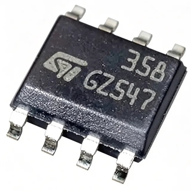
LM358DT - Dual Low Power Op Amp | STMicroelectronics | SOIC-8
The LM358DT is a dual operational amplifier from STMicroelectronics, designed for low-power, general-purpose applications. It operates from a single or split power supply ranging from 3V to 32V (or ±1.5V to ±16V), with a typical quiescent current of 350 µA per amplifier. The device is housed in an 8-pin SOIC (SO-8) package, making it suitable for space-constrained PCB designs. Data verified as of 2026-08-05. An operational amplifier (op-amp) is a high-gain voltage amplifier with differential inputs and a single-ended output. It is a fundamental building block in analog electronics, used for signal conditioning, filtering, and mathematical operations. The LM358 is part of the general-purpose op-amp family, which includes the LM324 (quad version) and LM393 (comparator). These devices are widely used in industrial, automotive, and consumer electronics due to their low cost, ease of use, and wide supply voltage range. Key features of the LM358DT include a wide supply voltage range (3V to 32V), low quiescent current (350 µA per amplifier), and a common-mode input voltage range that includes ground, allowing single-supply operation. The output stage can sink and source current, and the device is short-circuit protected. The LM358DT also features a typical input offset voltage of 2 mV and a gain-bandwidth product of 1.1 MHz, making it suitable for low-frequency signal processing. The LM358DT uses a bipolar transistor architecture with a class-AB output stage, providing low crossover distortion. The input stage is a PNP differential pair, which allows the input common-mode range to extend to the negative supply rail (ground in single-supply operation). This design enables direct sensing of signals near ground, a key advantage in battery-powered and single-supply systems. Typical applications include transducer amplifiers, DC gain blocks, active filters, and signal conditioning in industrial control systems. The LM358DT is also used in portable instrumentation, power supply monitoring, and automotive sensor interfaces. Its low power consumption makes it ideal for battery-operated devices. When designing with the LM358DT, ensure that the input common-mode voltage does not exceed the specified range, and provide adequate decoupling capacitors on the power supply pins. The output can drive loads down to 2 kΩ, but for heavier loads, consider using a buffer stage. The device is stable with capacitive loads up to 500 pF, but for larger loads, an external compensation network may be required. This page synthesizes distributor pricing, drop-in alternatives, and practical design notes not found in the STMicroelectronics datasheet, providing engineers with a comprehensive resource for selecting and using the LM358DT.
LM358M - Dual 32 V, 1 MHz Operational Amplifier | Texas Instruments
Texas Instruments LM358M is a dual, general-purpose operational amplifier with two independent channels, a 32 V maximum supply rating, 1 MHz gain-bandwidth product, and an 8-pin SOIC package. The device is designed for single-supply operation and is identified by distributor data as a standard dual operational amplifier in the SOIC-8 format. An operational amplifier is an analog signal-conditioning semiconductor device that uses high open-loop gain to amplify voltage differences. LM358M combines two amplifier channels in one package, allowing one IC to implement functions such as buffers, transimpedance stages, filters, comparators, sensor interfaces, and audio or industrial control blocks. Its dual-channel architecture can also reduce board area when both channels perform similar signal tasks. The verified listing specifies a 32 V supply-related operating class and 1 MHz gain-bandwidth product for the LM358M device. The supplied datasheet search results describe the LM358 family as internally frequency compensated for unity gain, with a large DC voltage gain of 100 dB, a wide power-supply range of 3 V to 32 V for LM358/LM358A, and an input common-mode voltage range that includes ground. These features make the part suitable for designs where the input signal is referenced to the supply ground. LM358M is packaged as an 8-SOIC, making it a practical surface-mount choice for compact analog boards. The dual amplifier organization can simplify routing when two related channels are required, while the general-purpose architecture supports broad industrial, consumer, instrumentation, and embedded-control applications. The SOIC package also supports conventional PCB assembly and inspection processes used for many analog signal-chain products. Typical applications include current sensing with a shunt amplifier, sensor-signal conditioning, active filtering, audio preamplification, comparator-style threshold detection, and low-frequency control loops. Because the verified data does not provide a complete numerical specification set, parameters such as exact input offset voltage, output-current limits, slew rate, common-mode limits, noise density, and temperature limits should be checked in the manufacturer datasheet before production release. When laying out LM358M, keep input and feedback traces short, place decoupling capacitors close to the supply pins, and avoid routing high-current return paths through sensitive analog nodes. For single-supply designs, confirm that the input common-mode range includes the signal range and that the load does not exceed the output-current capability stated in the selected device datasheet. This page consolidates verified distributor specifications, source links, package information, and practical design guidance.
LM358MX - Dual Operational Amplifier | Texas Instruments
The Texas Instruments LM358MX is a dual operational-amplifier device associated with the LM358 family. The supplied verified-web-data package did not return a manufacturer datasheet, distributor listing, or alternatives cross-reference, so the verified electrical ratings, package dimensions, temperature range, supply limits, pricing, and lifecycle status cannot be confirmed from the provided records. The LM358 family is commonly associated with single-supply, general-purpose dual-amplifier designs, but engineers should verify the complete LM358MX datasheet before releasing a PCB or production BOM. What is an operational amplifier? An operational amplifier is an analog active device that amplifies the difference between two input voltages while using feedback to control gain and bandwidth. A dual operational-amplifier package contains two amplifier channels and is classified as an amplifier IC within the broader semiconductor hierarchy. LM358-family devices are often considered for sensor conditioning, signal buffering, and low-frequency analog control, but the precise suitability of LM358MX for a particular application depends on verified specifications such as input common-mode range, output swing, supply current, offset voltage, slew rate, and noise. The available data does not identify the MPN suffix, package drawing, pin configuration, or ordering details. The LM358 suffix commonly denotes an SOIC-8-style variant, but that package identification is not present in the supplied verified records and therefore requires confirmation. The absence of verified data also prevents a reliable comparison with related LM358, LM2902, or competing dual-amplifier variants. Typical design evaluation should begin with the manufacturer's LM358MX datasheet and pinout. Review the recommended operating conditions, absolute maximum ratings, electrical characteristics, common-mode range, output-swing limits, and stability requirements. Confirm the exposed or non-exposed package dimensions and the PCB land pattern rather than relying on the MPN suffix alone. Applications commonly investigated for a dual operational amplifier include DC signal conditioning, transducer interfaces, active filtering, and low-frequency analog signal chains. These uses remain provisional until the LM358MX electrical limits, package geometry, and temperature ratings are verified. This page intentionally distinguishes confirmed sourcing information from engineering claims that still require datasheet confirmation. This page provides a structured place to compare the MPN, assess unavailable datasheet fields, identify same-family drop-in options, and review practical selection questions. For a production decision, use the manufacturer datasheet and current authorized-distributor inventory rather than inferred suffix data. The verified records were retrieved on 2026-10-29, but the underlying web-search operation returned a timeout and no component-specific result.

LM358N - Dual 32 V 1 MHz Op Amp | DIP-8 Amplifier
The Texas Instruments LM358N is a dual, general-purpose operational amplifier with two independent amplifiers, a 32 V rating, 1 MHz typical bandwidth, and an 8-pin through-hole DIP package. It is designed for single-supply operation and is widely used where low cost, moderate precision, and straightforward dual-amplifier integration are more important than rail-to-rail input or output performance. An operational amplifier is an amplifier IC that uses high open-loop gain to amplify the difference between its non-inverting and inverting inputs. In feedback configurations, the LM358N can provide voltage gain, buffering, filtering, summing, and current-control functions. It belongs to the hierarchy of operational amplifier, analog amplifier, analog IC, and semiconductor. The verified product information identifies the LM358-N as a dual, 32 V, 1 MHz op amp. The LM358N package is listed by distributors as an 8-pin mini-DIP or 8-pin PDIP package, depending on the manufacturer source. Because the supplied data does not include every electrical limit, several detailed parameters remain marked as data-needed rather than inferred. Each internal amplifier is designed for general-purpose signal conditioning. The device is suitable for industrial control, sensor interfaces, audio and communication circuits, power-control loops, transducers, and low-frequency analog signal chains. Its dual architecture reduces the number of IC packages required when two independent amplifier functions are needed. The most important design consideration is supply and input/output range. The 32 V maximum device rating does not mean every circuit should operate at 32 V. Designers must verify the selected manufacturer version, common-mode range, output swing, input bias behavior, noise, slew rate, and thermal limits before finalizing a design. The verified sources do not provide a complete, unified parameter table for this page. This page combines the verified manufacturer and distributor references, package references, and cross-reference search results with practical engineering guidance. It is intended to help engineers locate the datasheet, assess compatibility, and plan a validation review before purchasing or substituting LM358N.
LM358NG - Dual 1MHz Op Amp | onsemi | Signal Conditioning
onsemi LM358NG is a dual general-purpose operational amplifier with a 3 V to 32 V supply range, 1 MHz gain-bandwidth product, and 0.6 V/µs slew rate in an 8-pin PDIP package. The device provides two amplifier channels in one IC, uses a common-emitter output stage with capacitive load capability, and is designed for operation from either a single supply or split supplies. Its low-power architecture and input bias current of 100 nA make it suitable for battery-powered, industrial-control, sensor-conditioning, and general analog signal-processing circuits. An operational amplifier is an amplifier IC whose open-loop gain and feedback network determine the gain of a closed-loop circuit. The dual amplifier belongs to the hierarchy of analog amplifiers, signal-chain ICs, and semiconductors. Unlike a precision rail-to-rail amplifier, the LM358NG is primarily intended for conventional supply-voltage operation and can accept input common-mode voltages extending toward ground or the negative supply, VEE. This makes it useful in single-supply systems where signals remain near the lower supply rail. Key features include two amplifier sections, a 3 V to 32 V operating supply range, 1 MHz gain-bandwidth product, 0.6 V/µs slew rate, 100 nA input bias current, and 7 mV input offset voltage. The dual configuration reduces package count and board area when two independent analog functions are required. Commercial temperature operation is identified by the distributor listings, while the low-power drain supports battery-operated instrumentation where every milliampere affects useful runtime. The internal architecture provides useful behavior for low-frequency, cost-sensitive analog designs. Its approximately 1 MHz bandwidth permits operation well below audio frequencies and supports common feedback networks for amplification, filtering, comparison, and summing functions. The 0.6 V/µs slew rate is adequate for signals whose required full-scale transition time is not extremely short. As with any non-rail-to-rail amplifier, designers should verify input and output operating ranges against the actual supply voltages and signal amplitudes. Typical uses include low-side current sensing, sensor amplification, transducers, audio preamplifier stages, active filters, and general instrumentation. In a 5 V system, the dual structure can process two channels or use one section for filtering and the other for amplification. In split-supply circuitry, the common-mode input range extending toward ground or VEE supports bipolar-style signal conditioning without requiring a separate rail-to-rail input device. The primary design consideration is power-rail compatibility. The LM358NG supports 3 V to 32 V operation, but output swing and common-mode limits remain constrained by the supplies. PCB layout should keep input traces short, provide a solid ground plane, and place power-bypass capacitors close to the supply pins. Stable feedback components and adequate output isolation are also important when driving capacitive loads. This product page consolidates verified onsemi and distributor information, pricing context, package details, pin assignment, alternative-device guidance, and practical application notes. It is intended to help engineers evaluate whether the DIP-8 dual amplifier fits a new design or a repair before comparing it with other pin-compatible devices.

LM358PT - Dual 3-32V Op Amp, 1.1MHz | STMicroelectronics
The STMicroelectronics LM358PT is a dual general-purpose operational amplifier containing two independent, internally frequency-compensated amplifiers. Its 3 V to 32 V single-supply operating range, 1.1 MHz unity-gain bandwidth, 100 dB DC voltage gain, and low input common-mode voltage of 0.6 V make it suitable for general signal conditioning. The device is supplied in an 8-pin TSSOP surface-mount package. An operational amplifier is an analog integrated circuit that amplifies the voltage difference between its inverting and non-inverting inputs. The LM358 belongs to the dual-operational-amplifier category within the broader amplifier IC and analog semiconductor hierarchy. Its two independent channels can amplify AC or DC signals, buffer inputs, perform comparisons, and support feedback-based circuit functions. Internal frequency compensation simplifies stable operation without an external compensation network. The principal features of the LM358PT include two amplifier channels in one package, a wide 3 V to 32 V supply range, 1.1 MHz unity-gain bandwidth, and 100 dB large-signal DC voltage gain. Internally compensated operation supports practical use without external compensation capacitors. The 8-pin TSSOP package also provides a compact surface-mount option for industrial control, instrumentation, sensor interfaces, and consumer equipment where board area matters. Technically, the LM358PT is designed for single-supply operation while accepting input signals close to the lower supply rail. The verified 0.6 V input common-mode figure gives designers a concrete limit when working from a 3 V or 5 V rail. Its bandwidth is sufficient for many audio, control, and instrumentation signals, but it is not a high-speed precision op amp. Applications requiring very low offset, very low noise, rail-to-rail output, fast slew rate, or high DC accuracy should be reviewed against the device limits before production release. Typical uses include sensor-signal conditioning, active filtering, transducers, relay and solenoid drivers, audio and communications interfaces, and general control loops. The two channels can process related signals in a compact circuit or implement separate functions. Because output-current capability and slew-rate limits remain important in real designs, the load should be checked against the manufacturer's operating information rather than assumed from the wide supply range. A key design consideration is input common-mode range: the LM358PT can operate from 0.6 V above the negative supply, but it does not provide true rail-to-rail input or output swing. Designers should also account for the effects of supply bypassing, output loading, stability with capacitive loads, and the power dissipation created by the voltage difference across each amplifier. This product record combines manufacturer and distributor information with a practical selection guide, package-aware alternatives, comparison parameters, and implementation notes. It is intended to help engineers confirm footprint, electrical fit, sourcing status, and application suitability before selecting LM358PT for a PCB redesign or new design.
LM358QDRQ1 - Automotive Dual 1MHz Op-Amp SOIC-8 | Texas Instruments
The Texas Instruments LM358QDRQ1 is an automotive-grade, dual general-purpose operational amplifier qualified to AEC-Q100, delivered in an 8-pin SOIC (0.154 inch, 3.90 mm width) package on tape and reel. Each of the two amplifier channels offers a gain bandwidth product of approximately 1 MHz with rail-friendly output swing suited to single-supply operation, making it a workhorse signal-conditioning amplifier for 12V automotive and 5V industrial systems. An operational amplifier (op-amp) is a high-gain voltage amplifier with differential inputs and a single-ended output; within the component hierarchy it belongs to the amplifier IC family, under integrated circuits, and is a core building block of analog signal chains. Dual op-amps such as the LM358-Q1 integrate two independent channels in one package, halving board area versus two single amplifiers while sharing supply rails. Key features include two independent amplifier circuits, a 1 MHz class gain bandwidth, low input offset suitable for general-purpose sensing, operation from single or dual supplies, and AEC-Q100 automotive qualification with temperature grading that supports harsh under-hood environments. The wide supply range allows direct interfacing with battery-backed rails and regulated 5V logic domains. Architecturally, the LM358-Q1 family traces to the classic LM358 bipolar design updated for automotive quality systems, with TI manufacturing controls per its automotive flow; the related LMV358-Q1 variant adds rail-to-rail output for low-voltage rails per the LMV321-Q1/LMV358-Q1/LMV324-Q1 datasheet. Typical applications include automotive sensor signal conditioning, current-sense amplification front-ends, active filters, comparators and level shifters, and battery-management monitoring stages in vehicle ECUs and industrial controllers. Design tip: with a 1 MHz GBW, keep closed-loop gains modest (10x or below) to preserve bandwidth and phase margin; check the output swing versus load, since the classic LM358 output does not reach the positive rail.