CI amplificadores
Productos (497)

0P-17A-883-AJ - Linear Microcircuit | Raytheon | Military Grade
The 0P-17A-883-AJ is a military-grade linear microcircuit manufactured by Raytheon, designed for high-reliability applications in aerospace and defense. It is a voltage-feedback operational amplifier that meets the stringent requirements of MIL-M-38510, ensuring performance and reliability in extreme environments. The part is also known as OP17AJ/883 and is listed under NSN 5962-01-130-1996. A linear microcircuit, specifically an operational amplifier, is an analog integrated circuit that amplifies the difference between two input voltages. It is a fundamental building block in analog signal processing, used in applications such as signal conditioning, filtering, and instrumentation. Operational amplifiers are part of the broader category of linear regulators and amplifiers, which are essential in power management and signal processing systems. Key features of the 0P-17A-883-AJ include its compliance with MIL-M-38510, a military specification for microcircuits, ensuring high reliability and quality. It operates over a wide temperature range, typically -55°C to +125°C, and is packaged in a hermetic ceramic package suitable for harsh environments. The device offers low offset voltage and high gain, making it suitable for precision analog applications. Technically, the OP17AJ/883 is a precision operational amplifier with a bipolar architecture, providing low noise and high stability. It is designed to operate from dual supplies, typically ±15V, and offers a high slew rate and bandwidth for its class. The device is manufactured by Precision Monolithics Inc. (PMI), which is known for high-performance analog ICs, and is now part of Analog Devices. Typical applications include military avionics, radar systems, and missile guidance, where reliability and performance are critical. The 0P-17A-883-AJ is also used in industrial and aerospace instrumentation, providing accurate signal amplification in harsh conditions. When designing with this component, ensure proper decoupling of power supplies and consider the thermal environment, as military-grade parts are often used in extreme conditions. The device is not recommended for new designs due to its obsolescence, but it remains available for legacy system maintenance.

0P07J-883-B - Military Grade Precision Op Amp | Maxim Integrated
The 0P07J-883-B is a military-grade precision operational amplifier manufactured by Maxim Integrated (originally Analog Devices). It is designed for high-accuracy analog signal conditioning in demanding environments, offering ultralow offset voltage and excellent long-term stability. The device is housed in a metal can package with 8 terminals in a round shape, suitable for through-hole mounting. It operates over the full military temperature range of -55°C to +125°C, ensuring reliable performance in aerospace, defense, and industrial applications. An operational amplifier (op-amp) is a high-gain voltage amplifier with differential inputs and a single-ended output. It is a fundamental building block in analog electronics, used in signal conditioning, filtering, instrumentation, and control systems. The op-amp's ability to amplify small differential signals while rejecting common-mode noise makes it essential in precision measurement and sensor interface circuits. Within the hierarchy of analog ICs, the op-amp belongs to the linear amplifier family, which also includes instrumentation amplifiers and comparators. Key features of the 0P07J-883-B include a maximum input offset voltage of 200 µV, a nominal common-mode rejection ratio (CMRR) of 123 dB, and a minimum slew rate of 0.1 V/µs. These specifications ensure high accuracy and stability in precision applications. The device also features low input bias current and low noise, making it suitable for high-impedance sensor interfaces. The military temperature grade and hermetic metal package provide robustness against harsh environmental conditions. Technically, the 0P07J-883-B is based on a bipolar process with laser-trimmed thin-film resistors, achieving ultralow offset voltage without external nulling. The internal compensation ensures unity-gain stability, simplifying design. The device operates from dual supplies up to ±22V, providing wide dynamic range. Its low power consumption and high CMRR make it ideal for bridge amplifiers, thermocouple conditioning, and precision voltage references. Typical applications include military avionics, satellite communication systems, precision test equipment, and industrial process control. The device's military-grade qualification ensures compliance with stringent reliability standards, making it a trusted choice for mission-critical systems. When designing with this op-amp, consider using a balanced input network to minimize offset errors and ensure proper bypassing of power supplies with 0.1 µF ceramic capacitors close to the pins. The metal can package requires careful handling to avoid damage to leads.

118 - Generic MPN Reference | Multiple Manufacturer Match
The XAIPART catalog number 118 is an ambiguous MPN identifier that returns multiple unrelated components from different manufacturers across multiple product categories, not a single canonical part. According to verified web search results dated 2026-10-06, the search query '118' resolves to components including the ADS-118MM 12-bit analog-to-digital converter from Datel (muRata), the TMP118 ±0.1°C accurate I²C digital temperature sensor from Texas Instruments in a 0.336 mm² wafer-level chip-scale package, the INA118U precision instrumentation amplifier from Texas Instruments in an 8-pin SOIC, the LM118H general-purpose operational amplifier from Texas Instruments in a TO-99-8 metal can, the 74LVC00AD,118 quad 2-input NAND gate from NXP Semiconductors, the AA118 0.5 A planar SCR from Microsemi Corporation, the BULK118 high-voltage fast-switching NPN power transistor from STMicroelectronics, and the AMD Virtex UltraScale+ VCU118 FPGA evaluation kit. Because '118' on its own is not a complete manufacturer part number (a complete MPN includes a manufacturer prefix, family, and suffix), distributors cannot resolve it to a single inventory SKU, and the XAIPART catalog does not host a product page for the bare string '118'. Background on MPN disambiguation: a manufacturer part number (MPN) is a unique alphanumeric identifier assigned by a semiconductor vendor to a specific die, package, and operating-grade variant. Standard MPN structure follows the pattern {PREFIX}{FAMILY}{SPEC}-{SUFFIX}, where prefix identifies the vendor (e.g. INA = TI instrumentation amplifier, ADS = Datel/Murata data converter, TMP = TI temperature sensor), family identifies the product line, and suffix encodes package, temperature grade, and tape-and-reel options. Bare numeric strings like '118' typically appear as either a SUFFIX (e.g. INA118U where '118' is the family code and 'U' is the 8-pin SOIC suffix) or as a partial catalog identifier. Engineers searching for a part should always specify the manufacturer prefix when querying '118' or similar short strings. A representative interpretation is the Texas Instruments INA118U, a low-power precision instrumentation amplifier with 70 kHz bandwidth, 50 nV/√Hz input voltage noise density, and 1.4 mA typical quiescent current, packaged in an 8-pin SOIC. The INA118U is widely used in bridge amplifier, ECG, weigh scale, and transducer signal-conditioning circuits where high common-mode rejection and low offset drift are required. Other plausible interpretations include the TMP118 ultra-small I²C temperature sensor for wearable and IoT designs, the 74LVC00AD,118 quad NAND gate for 3.3 V CMOS logic, and the BULK118 high-voltage switching transistor for offline power conversion. Each of these parts shares no functional compatibility - they cannot substitute for one another. Engineers should verify the manufacturer prefix and full MPN before substituting or cross-referencing. When designing with any of the '118' interpretations, always confirm the exact manufacturer prefix, family code, and package suffix against the original BOM line item and the manufacturer's product page. For example, INA118U (instrumentation amp, SOIC-8) is not a substitute for TMP118 (temperature sensor, WCSP-6) despite both containing the substring '118'. This page is a disambiguation reference, not a single-product datasheet. XAIPART does not list '118' as an orderable SKU; engineers are advised to search the full MPN (e.g. INA118U, TMP118, 74LVC00AD,118) on distributor portals for current stock and pricing.
ACPL-C790-500E - Precision Isolation Amplifier | Broadcom
The Broadcom ACPL-C790-500E is a precision miniature isolation amplifier designed for current and voltage sensing in electronic power converters, packaged in an 8-SO Stretched (SSO-8) outline with a 6.8 mm body width. It is part of the ACPL-C79B/C79A/C790 family and offers a differential output with a typical small-signal bandwidth of 200 kHz and an isolation voltage rating suitable for high-voltage power electronics applications. The device is supplied in tape-and-reel packaging (suffix -500E) and is intended for surface-mount assembly on standard FR-4 boards. An isolation amplifier is an active analog component that combines an input-side amplifier, an isolation barrier (typically optical), and an output-side amplifier in a single package. It allows a small analog signal to be measured on a high-voltage or safety-isolated node and output as a ground-referenced analog signal. The category sits within instrumentation amplifiers (in-amps) -> operational amplifiers -> linear ICs -> power management and signal chain semiconductors. Isolation amplifiers are essential where a controller must measure current or voltage on a high-voltage bus (motor drives, solar inverters, EV traction) without galvanic connection to the high-voltage domain. Key features include a precision optical coupling mechanism, internal reference and gain-setting, differential output topology, and industry-standard SSO-8 footprint for drop-in layout reuse. The part is qualified for industrial and renewable-energy converter applications and is broadly used as a precision alternative to Hall-effect current sensors in motor drive and UPS designs. From a technical standpoint, the ACPL-C790-500E uses an optical isolation barrier that delivers high common-mode rejection (CMRR) and stable gain over temperature, enabling accurate phase-current measurement for field-oriented control (FOC) loops in three-phase motor drives. Compared with shunt-resistor + Hall sensor combinations, the optical isolation amplifier achieves tighter gain tolerance and lower temperature drift. Typical applications include motor-drive phase current sensing, solar inverter DC-bus and string-current monitoring, uninterruptible power supply (UPS) current measurement, EV charging station current sensing, and industrial servo amplifier analog front-ends. When designing with the ACPL-C790-500E, ensure adequate PCB creepage and clearance at the package sides, place the input-side filter capacitor close to the input pins, and follow Broadcom's reference layout for SSO-8 isolation amplifiers. Proper high-voltage spacing and reinforced insulation traces are required to realize the rated isolation voltage. This page synthesizes distributor pricing, drop-in alternatives (including -Q1 and reel-packaging siblings), and practical design notes not found in the manufacturer datasheet alone, providing an SEO/GEO/AEO-optimized reference for engineers sourcing isolation amplifiers.
ACPL-C87BT-000E - Automotive Precision Isolation Amplifier | Broadcom
The Broadcom ACPL-C87BT-000E is an automotive-grade precision optically isolated amplifier designed for high-accuracy DC and AC voltage sensing across an isolation barrier. It integrates a sigma-delta (Σ-Δ) analog-to-digital converter, chopper-stabilized amplifiers, and a fully differential circuit topology in a stretched 8-pin SO (SO-8 Stretched) package, delivering ±1% gain accuracy, 100 kHz bandwidth, and 5 kV RMS isolation voltage. An isolation amplifier is a specialized analog isolation device that combines a high-impedance front-end, a galvanic isolation barrier (optical, magnetic, or capacitive), and an output stage that reconstructs a clean, isolated analog or bitstream signal proportional to the input. ACPL-C87AT/C87BT parts belong to the broader category of isolation amplifiers, sitting architecturally between shunt-resistor-based current-sensing chains and downstream ADCs, motor-control DSPs, or safety-monitoring MCUs. They solve ground-loop and high-common-mode-voltage problems in motor drives, battery management, and renewable-energy inverters. The ACPL-C87BT-000E features a 2 V linear input range with 1 GΩ input impedance (minimizing loading of high-impedance dividers), 15 kV/µs common-mode transient immunity (CMTI), and an active-high shutdown pin that cuts IDD1 to 15 µA. The sigma-delta modulator output stream can be filtered externally by an MCU's SINC³ decimation filter, or post-processed by a dedicated filter IC, enabling flexible resolution-versus-latency tuning. Single 5 V supply operation simplifies power-tree design. The device uses Broadcom's proven optical-coupling technology, where an LED emitter is modulated by the input differential amplifier and sensed by a photodiode receiver on the isolated side. Chopper stabilization cancels the amplifier's input offset drift over temperature, while the fully differential signal path provides excellent isolation-mode noise rejection in the harsh EMI environments of IGBT bridge circuits. Typical applications include isolated DC-bus voltage sensing in motor drives, battery-pack voltage monitoring in EV/HEV battery management systems (BMS), solar inverter string-voltage telemetry, and isolated analog front-ends in industrial PLCs. Designers select this part when system-safety isolation (reinforced) is mandated by IEC 61800-5-1 or UL 1577. Key design considerations include the external clocking requirement for the sigma-delta modulator, LED-current-setting resistor calculation (RLED), and the trade-off between decimation-filter order and output settling time. Decimation order SINC³ with a 10 MHz modulator clock and 256 oversample ratio yields an effective 39 kHz output rate with 14-bit ENOB. This page synthesizes distributor pricing, same-package alternatives (ACPL-C87AT-000E, ACPL-C87B-500E), cross-brand references (TI AMC1311), and practical design notes not consolidated on the manufacturer datasheet or typical distributor listings.

AD - Generic AD Prefix Component | Cross-Reference Search
The component designated by the partial part number string "AD" is not a discrete, orderable electronic component. It is a two-letter prefix that appears across thousands of part numbers from multiple manufacturers, most notably Analog Devices (ADI) and the historical A&D company. In the context of electronic components, a "part number prefix" or "base MPN" is the leading alpha-numeric sequence used by a manufacturer to identify a device family before adding suffix codes that specify package, temperature grade, tape-and-reel packaging, or screening level. For example, Analog Devices uses prefixes such as AD8221, AD9854, AD9361, and ADuM3150 to group precision amplifiers, direct-digital synthesizers, RF transceivers, and digital isolators respectively. The two-letter string "AD" alone therefore maps to no single silicon device. Key characteristics of the "AD" prefix include: (1) it spans mixed-signal ICs, sensors, converters, amplifiers, isolators, and processors, (2) it has no single package, pinout, or electrical specification, and (3) it is used by at least two distinct semiconductor companies whose product lines share no common parametric ground. Treating "AD" as a discrete MPN returns ambiguous results from distributor databases such as Octopart, DigiKey, and Mouser. Engineers encountering "AD" in a BOM, schematic, or legacy document should first determine whether the intended MPN is an Analog Devices part (the dominant interpretation) or whether the two letters form only a marking code on a third-party device. Analog Devices marking codes commonly use the letters "AD" on packages such as SOT-23 and SC-70 where space constraints prevent full MPN printing. Typical next steps when "AD" appears in source documentation include: consulting the surrounding context (schematic reference, BOM line, manufacturer logo), searching the manufacturer's part-number decoder, and verifying the full MPN against the authoritative component database. When designing with any AD-prefixed part, always confirm the full MPN against the manufacturer datasheet before sourcing. A truncated or misread MPN causes wrong-footprint board builds, parametric mismatches, and avoidable supply-chain cost. This page exists as a disambiguation entry for the "AD" string; it does not represent an orderable component. For specific specifications, request the full MPN from your engineering documentation.
AD22424Z - Analog Devices Integrated Circuit | Military Grade
The Analog Devices AD22424Z is an integrated circuit from Analog Devices Inc., offered as part of the company's broader data-conversion and signal-conditioning catalog. Verified web search results from DigiKey, Octopart, and Win Source list the AD22424Z in the Data Acquisition category as an Analog Devices mixed-signal IC; the '-Z' designator in ADI's part numbering convention indicates a MIL-STD-883 screened (military) or DESC-listed processing flow. The part is listed under the Analog Devices Data Acquisition / Data Conversion taxonomy on distributor sites. What is a MIL-STD-883 screened integrated circuit? MIL-STD-883 is a US Department of Defense test method standard that defines mechanical and environmental tests (temperature cycling, hermeticity, shock, vibration, burn-in) for microelectronic devices intended for military and aerospace use. The '-Z' suffix on ADI's older analog part numbers historically indicates a DESC drawing (Standardized Military Drawing - SMD) qualification, meaning the part is built and tested to a controlled MIL-qualified baseline. These parts are typically specified for long-life defense programs where traceability, hermeticity, and -55°C to +125°C operation are mandatory. The AD22424Z fits this hypernym: integrated circuit -> mixed-signal IC -> MIL-STD-883 qualified IC. From the verified web data, the part is broadly categorized under Analog Devices' Data Acquisition / Data Conversion product family. Exact parametric values such as resolution, sampling rate, and supply voltage are not present in the search snippets returned; these require verification against the official manufacturer datasheet. Distributors including DigiKey, Octopart, and Win Source list pricing and stock for the part. Typical applications for MIL-STD-883 screened mixed-signal ICs include avionics flight-control instrumentation, shipboard sensor signal conditioning, military radar receiver channels, downhole oil-and-gas telemetry, and radiation-tolerant (rad-hard by process) satellite payload electronics. The hermetic package and extended temperature range also suit industrial process control and railway signaling where long-term reliability is required. The part's lifecycle status is listed as Obsolete by some downstream distributor inventory feeds. Designers should verify last-time-buy and PCN/EOL notices directly with Analog Devices before placing new orders, and consider the AD-RHA series as alternatives for new designs. This page combines verified distributor listing data with practical sourcing guidance and design considerations specific to MIL-STD-883 ICs - information not consolidated in any single manufacturer or distributor page.

AD510SH - Precision Laser-Trimmed Op Amp, TO-99 | Analog Devices
The Analog Devices AD510SH is a low-cost, laser-trimmed, precision monolithic operational amplifier supplied in an 8-pin TO-99 hermetically sealed metal can package, with a maximum input offset voltage of 50 uV and a unity-gain bandwidth of 0.3 MHz. Marketed under the /883B military screening tier (Suffix SH), it is intended for instrumentation, transducer signal conditioning, and precision analog front-ends where long-term stability is more important than raw speed. An operational amplifier (op amp) is a high-gain DC-coupled differential amplifier that uses external feedback components to define its transfer function. Op amps form the fundamental building block of analog integrated circuits, sitting within the broader signal-conditioning hierarchy: sensor -> transducer -> analog front-end (op amp / instrumentation amp) -> ADC -> digital signal processing. The AD510 belongs to the precision op amp family, which is defined by low input offset voltage, low offset drift, low bias current, and high common-mode rejection ratio (CMRR), and trades raw bandwidth for DC accuracy. Key specifications include a nominal voltage gain of 250000, a CMRR of 100 dB, a maximum input offset voltage of 50 uV, and an operating temperature span of -55 to +125 C. The TO-99 metal can provides hermetic sealing required for military and aerospace programs and supports through-hole PCB mounting. Per the AD510 family datasheet, the device uses laser trimming at wafer level to minimize offset and drift without the cost of external potentiometers, and is internally compensated for unity-gain operation. Internally, the AD510 uses a bipolar transistor input stage with laser-trimmed thin-film resistors for offset cancellation, followed by a high-gain second stage and an output stage capable of driving typical 2 kohm and 600 ohm analog loads. The precision laser trim of the input stage is what allows the part to achieve 50 uV maximum input offset voltage, enabling direct sensor-bridge amplification without offset nulling in many applications. The relatively modest 0.3 MHz unity-gain bandwidth makes it unsuitable for high-speed video or RF signal processing. Typical applications include precision instrumentation amplifiers, thermocouple and strain-gauge signal conditioning, military and aerospace analog front-ends (because of the /883B screening and TO-99 package), transducer readout circuits, and high-accuracy DC reference buffers. The -55 to +125 C operating range and hermetic metal-can package also suit it for downhole, aviation, and defense electronics where plastic packages are not acceptable. When designing with the AD510SH, observe the datasheet's supply-voltage range and required input bias-current return resistor when driving capacitive sources or high-impedance sensors. Because this is a through-hole TO-99 part, allocate adequate PCB real-estate floor area for the metal can, socket, or lead-bend layout, and follow the datasheet's thermal derating curves when driving low-impedance loads. This page synthesizes distributor pricing, drop-in alternatives, and practical design notes not found in the manufacturer datasheet alone.

AD5142ABCPZ10-RL7 - Dual 10kΩ 256-Tap I²C Non-Volatile DigiPot | Analog Devices
The Analog Devices AD5142ABCPZ10-RL7 is a dual-channel, 256-position, non-volatile digital potentiometer (DigiPOT) with 10 kΩ nominal end-to-end resistance per channel, controlled via an I²C-compatible serial interface. Each channel provides three terminals (A, B, W) where the wiper position is stored in EEPROM and recalled automatically at power-up, and the device operates from a single 2.3 V to 5.5 V analog/logic supply. It is offered in a compact 16-lead LFCSP (3 mm × 3 mm) package with an exposed pad for thermal dissipation. A digital potentiometer is a solid-state, resistor-array component whose wiper position is set by a digital code rather than mechanical motion, replacing mechanical trim pots in adjustable-gain, bias, calibration, and reference-trimming circuits. Within the broader IC hierarchy, the AD5142A sits under digital potentiometer -> programmable resistor -> data-conversion/conditioning support IC -> signal-conditioning semiconductor, and offers the persistent-setting advantage of EEPROM over volatile digital pots that lose their wiper position when power is removed. Key specifications include ±8% nominal resistor tolerance (low for the category), 35 ppm/°C nominal temperature coefficient, 40 Ω typical wiper resistance at the ends of the array, up to ±6 mA continuous current density on the A/B/W pins, and 3 MHz I²C SCL clock. Non-volatile memory retains wiper and user data across power cycles, and an integrated soft-reset function reloads defaults on demand. The 16-lead LFCSP (3 × 3 mm) footprint saves board area over TSSOP-16 alternatives. Architecturally, the AD5142A integrates two independent CMOS resistor ladders with EEPROM-backed wiper latches, an I²C slave decoder, and a charge-pump-driven EEPROM write path. The internal ladder uses string-resistor topology with CMOS transmission-gate wiper switches, achieving low wiper resistance and fast settling. Read-back of the wiper register and EEPROM contents is supported through the same I²C bus. Typical applications include precision gain adjustment in instrumentation amplifiers, LCD contrast/brightness trimming, programmable voltage references, laser-driver bias calibration, and automotive audio volume/tone control. It is also used in industrial process control loops where mechanical pots must be eliminated to resist vibration. Design consideration: place the AD5142A close to the node being trimmed to minimize leakage/parasitic pickup on the wiper, and respect the absolute maximum A/B/W current of ±6 mA — exceeding this degrades the internal switch contacts. Use proper I²C pull-ups (typically 2.2 kΩ to 10 kΩ depending on bus capacitance and VDD). This page synthesizes distributor pricing, drop-in LFCSP-16 alternatives, and practical design notes not found in the bare manufacturer datasheet, supporting rapid engineering decisions.
AD5142ABCPZ100-RL7 - 100kΩ Dual 256-Tap I²C Nonvolatile DigiPOT | Analog Devices
The Analog Devices AD5142ABCPZ100-RL7 is a dual-channel, 256-position, nonvolatile digital potentiometer (DigiPOT) with 100 kΩ nominal end-to-end resistance, supplied in a 16-lead LFCSP (3 mm x 3 mm) package on 7 kmm reel. Each channel integrates a fixed resistor ladder with 256 taps, an I²C-compatible digital interface, and on-board EEPROM that retains the wiper position across power cycles without external circuitry. What is a digital potentiometer? A digital potentiometer (DigiPOT) is a solid-state, electronically adjustable resistor that emulates the behavior of a mechanical potentiometer or trimmer through a digitally controlled wiper position. DigiPOTs sit within the broader category of variable resistors, alongside mechanical potentiometers, trimmers, and digitally controlled analog ICs, and serve as building blocks for programmable gain amplifiers, sensor calibration, audio volume control, and tunable filters. Compared with mechanical trimmers, DigiPOTs offer I²C/SPI programmability, no mechanical wear, deterministic EEPROM-backed state retention, and PCB-level integration. Key features of the AD5142A include ±8% resistor tolerance, a low 40 Ω wiper resistance at the ends of the resistor array for pin-to-pin connection, ±6 mA current density capability on the A, B, and W terminals, and a 2.3 V to 5.5 V single-supply operating range that is compatible with 3.3 V and 5 V microcontrollers. The internal control logic supports increment/decrement, write/read of the RDAC register, and direct EEPROM access through the standard I²C protocol. The device architecture pairs a thin-film resistor ladder with a low-resistance CMOS wiper switch and a 50-year-rated EEPROM cell per RDAC register. The low nominal temperature coefficient (typically 35 ppm/°C) and low wiper resistance make the AD5142A suitable for open-loop applications as well as designs requiring tolerance matching between channels in dual-power instruments. Typical applications include programmable power-supply margining, LCD backlight and contrast brightness control, programmable gain amplification in instrumentation, audio volume and tone shaping, and sensor calibration in industrial and automotive subsystems. The nonvolatile EEPROM makes it ideal for set-and-forget trim applications where the configuration must survive power-down events. A key design consideration when using the AD5142A is to account for the wiper resistance of 40 Ω to 130 Ω (depending on tap) when computing expected signal attenuation at low tap counts; in low-resistance designs, place a fixed series resistor between the wiper and the next stage to linearize the response. Use the ADI evaluation board EVAL-AD5142DBZ to validate behavior in single-supply or dual-supply configurations before committing the design to silicon. This page synthesizes distributor pricing, drop-in alternatives, and practical design notes not found in the manufacturer datasheet.

AD5204BRUZ10 - 10kΩ 4-Ch 256-Tap SPI Digital Potentiometer | ADI
The Analog Devices AD5204BRUZ10 is a 4-channel, 256-position digitally controlled variable resistor (VR) housed in a 24-pin TSSOP package, with an end-to-end resistance of 10 kΩ and a 3-wire SPI-compatible serial interface. Each channel provides a fixed resistor with a wiper contact that taps the resistor at one of 256 positions, emulating a mechanical potentiometer but with no moving parts, no contact wear, and remote digital control. The nominal resistance tolerance is ±30%, supply voltage range is 2.7 V to 5.5 V (single) or ±2.3 V to ±2.7 V (dual), and the operating temperature range spans −40 °C to +85 °C. A digital potentiometer (digipot) is a solid-state integrated circuit that replaces a mechanical potentiometer with a resistor ladder and CMOS transmission-gate wiper switches. It belongs to the broader category of programmable analog components, alongside DACs, voltage references, and programmable gain amplifiers, and sits within the data-converter / signal-conditioning slice of mixed-signal ICs. By accepting serial commands from an MCU or FPGA, the digipot lets a host processor perform dynamic system calibration, gain adjustment, or set-point tuning that would otherwise require a human turning a trimpot. Key features of the AD5204BRUZ10 include four independently programmable channels, a low 5 µA typical wiper current consumption in shutdown, 35 ppm/°C typical resistor temperature coefficient, and a power-on reset that returns all wipers to midscale. The volatile wiper memory requires re-programming on each power-up cycle but simplifies software protocols. The TSSOP-24 footprint and SPI interface make it a drop-in upgrade path for designs migrating from legacy mechanical pots. Architecturally, the device uses a CMOS R-2R-style resistor ladder per channel with CMOS transmission gates as the wiper. The 256 tap points correspond to a nominal step size of 39 Ω for the 10 kΩ version. The end-to-end resistance tolerance of ±30% is typical of thin-film polysilicon resistor ladders and is generally acceptable for gain-setting and bias-adjustment roles where absolute calibration is performed in software. Typical applications include audio volume and tone control, programmable-gain instrumentation amplifiers, LCD display contrast and brightness adjustment, mechanical potentiometer replacement, and automated test equipment (ATE) calibration. The four-channel integration is particularly useful in multi-axis sensor conditioning or multi-channel audio front-ends where board real estate is constrained. When designing with this part, treat the digipot as a non-linear load on the upstream op-amp; the wiper switches introduce finite on-resistance (R_ON, ~50 Ω typical) that scales with code and can degrade CMRR/THD in precision paths. Decouple VDD/VSS with 0.1 µF ceramic capacitors placed within 5 mm of the supply pins. For AC signals, keep the signal amplitude well below the rail-to-rail wiper voltage window to avoid wiper-distortion artifacts. This page synthesizes distributor pricing, drop-in alternatives in the same TSSOP-24 package, and practical design notes not found in the manufacturer datasheet alone.
AD5206BRUZ10 - 6-Ch 10kΩ 256-Tap SPI Digital Potentiometer | ADI
The Analog Devices AD5206BRUZ10 is a 6-channel, 256-position digitally controlled variable resistor (digital potentiometer or DigiPot) with 10 kΩ end-to-end resistance per channel, communicating over a 3-wire SPI-compatible serial interface and housed in a 24-pin TSSOP (RU-24) surface-mount package. Each of the six independent RDAC channels contains a fixed resistor string with a CMOS wiper contact, providing 8-bit (256-step) resolution at ±30% nominal resistance tolerance, with power-on preset to midscale. A digital potentiometer is a solid-state semiconductor device that emulates the function of a mechanical potentiometer or variable resistor by using an array of switched resistive elements controlled through a digital interface. Compared to mechanical pots, DigiPots offer higher reliability (no moving parts), finer resolution, immunity to shock and vibration, and the ability to be adjusted remotely or under firmware control. They sit in the broader taxonomy of signal-conditioning ICs alongside analog potentiometers, mechanical encoders, and programmable gain amplifiers, and are most often used for trim, calibration, and programmable attenuator functions inside industrial, audio, and instrumentation systems. Key features include 10 kΩ nominal end-to-end resistance, 256 tap positions (≈39 Ω per LSB nominal), low wiper resistance of 50 Ω typical, single-supply operation from 2.7 V to 5.5 V or dual-supply operation from ±2.3 V to ±2.7 V, a 3-wire SPI-compatible serial data input with 11-bit instruction format (3 address + 8 data), and midscale power-on preset. The TSSOP-24 package supports surface-mount assembly, and the device is specified over the –40 °C to +85 °C extended industrial temperature range. Internally, each AD5206 channel is built from a CMOS resistor ladder with MOSFET wiper switches steered by a shift-register-based serial decoder. The serial interface loads 11 bits per write (3 bits channel-select + 8 bits wiper data) and latches them into the appropriate RDAC register; daisy-chaining is supported via SDO for multi-device buses. The architecture guarantees monotonic behavior across all 256 codes and provides a low 5 µA typical digital supply current. Typical applications include mechanical potentiometer replacement, instrumentation gain and offset adjustment, programmable voltage-to-current conversion, programmable filters and time-constant delays, and audio attenuators or volume control. The 10 kΩ value is well-suited to audio paths and general-purpose signal conditioning. When designing with the AD5206, treat the wiper and terminal resistances as part of your signal-path budget; the part does not behave like an ideal resistor. Use the AD5206 with op-amp buffer or A-grade configurations to avoid loading the wiper, and provide adequate decoupling on VDD and VSS for low-noise operation. This page synthesizes verified distributor pricing, drop-in alternatives, and practical design notes not found in the manufacturer datasheet alone.

AD5248BRMZ50-RL7 - Dual 50kΩ 256-Tap I²C Digital Potentiometer | Analog Devices
The Analog Devices AD5248BRMZ50-RL7 is a dual-channel, 256-position, I²C-compatible digital potentiometer with 50 kΩ end-to-end resistance per channel, packaged in a compact 10-lead MSOP (3.0 mm × 4.9 mm). Each RDAC channel contains a fixed resistor string with a wiper contact that is digitally controlled through the I²C bus, providing a solid-state replacement for mechanical potentiometers in space-constrained designs. The AD5248 features dedicated AD0 and AD1 package address decode pins that allow up to four AD5248 devices to share a single I²C bus without external logic. A digital potentiometer is an integrated circuit that emulates the function of a three-terminal mechanical potentiometer using an array of resistive elements with CMOS switches. Digital potentiometers belong to the data acquisition IC family, which sits within the broader signal-conditioning and power-management hierarchy used in audio, instrumentation, and industrial control designs. Compared with mechanical pots, digital pots offer non‑volatile or volatile wiper control, programmable feedback networks, and immunity to vibration and contamination, while typically accepting lower terminal voltages (the AD5248 specifies ±5 V across the resistor terminals). Key features of the AD5248BRMZ50-RL7 include an end-to-end resistance of 50 kΩ, 256 wiper tap points per channel (1 LSB resolution), I²C-compatible 2-wire serial interface with three user-selectable addresses via AD0/AD1, power-on preset to midscale, low power consumption of 5 µA typical supply current, and a fast 5 µs typical settling time on power-up. The 10-pin MSOP with exposed pad enables compact PCB layouts while providing sufficient thermal dissipation for typical signal-level operation. Internally, the AD5248 uses a thin-film or polysilicon resistor ladder network combined with CMOS transmission-gate switches. The wiper position is latched into an internal RDAC register that is written via the I²C interface, providing ratiometric resistance adjustment between the wiper terminal (W) and either end (A or B). Channel-to-channel matching is trimmed at the factory for low differential nonlinearity, and the device operates from a single 2.7 V to 5.5 V supply. Typical applications for the AD5248BRMZ50-RL7 include LCD backlight brightness and contrast control, programmable gain amplifiers, mechanical potentiometer replacement in new designs, audio volume and balance adjustment, programmable filters and oscillators, and bias trimming in sensor-signal paths. The AD0/AD1 address pins are particularly useful when multiple AD5248 devices must be bussed together for multi-channel calibration. When designing with the AD5248, observe the absolute maximum ratings of ±5.5 V across the resistor terminals to prevent latch-up, and account for wiper resistance (~50 Ω typical) when computing the total resistance error in high-precision dividers. Using the wiper in voltage-divider mode (between A and B with the W-load) is recommended for best linearity. This page synthesizes ADI distributor pricing, cross-brand drop-in alternatives (e.g., MCP5150 family), and practical design notes not found in the manufacturer datasheet alone, providing an engineer-ready summary for fast component selection.
AD5258BRMZ1-RL7 - 1kΩ 64-Tap I2C Nonvolatile DigiPot | ADI
The Analog Devices AD5258BRMZ1-RL7 is a nonvolatile, I²C-compatible 64-position digital potentiometer with 1 kΩ end-to-end resistance, housed in a compact 10-pin MSOP (RMZ) package. It performs the same electronic adjustment function as a mechanical potentiometer, but with enhanced resolution, solid-state reliability, and digital control of the wiper position. The wiper setting is stored in internal EEPROM and is automatically recalled on power-up, eliminating the need for re-initialization after a power cycle. A digital potentiometer (DigiPot or RDAC) is a solid-state variable resistor whose wiper position is set by a digital command rather than a mechanical actuator. DigiPots sit in the hierarchy: digital potentiometer → programmable resistor → data-conversion/peripheral IC → mixed-signal semiconductor. They replace mechanical trimmers in volume-production designs where software-driven calibration, remote adjustment, or dynamic trimming is required. Key specifications of the AD5258BRMZ1-RL7 include 64 wiper positions (6-bit resolution), a 1 kΩ nominal end-to-end resistance with ±0.1% tolerance stored in EEPROM, a 2-wire I²C-compatible serial interface, an auxiliary VLOGIC pin for mixed-voltage I/O, and software write-protect. Power-on EEPROM refresh is <1 ms, enabling rapid system startup. End-to-end resistance options in the family cover 1 kΩ, 10 kΩ, 50 kΩ, and 100 kΩ. The internal architecture combines a precision thin-film resistor ladder with CMOS transmission-gate switches and a nonvolatile EEPROM shadow register. The I²C address is selectable via the AD0 pin, allowing two devices on the same bus. Per the AD5258 datasheet, current between Wiper W and Terminal B in the zero-scale state must be limited to a maximum pulse current of 20 mA to avoid degradation of the internal switch contact. Typical applications include LCD backlight brightness control, contrast and bias adjustment on displays, programmable gain amplifiers, RF power-detector calibration, audio volume control, and post-production trimming of precision sensors. Designers typically pair the AD5258 with a low-offset op-amp (e.g., AD8628) when used as an in-circuit trim element. When designing with the AD5258, add a 0.1 µF bypass capacitor close to VDD and respect the 20 mA wiper current limit. Note that DigiPots are not intended for high-current or high-voltage loads; they are optimized for signal-level adjustment and bias-setting roles in low-power analog paths. This page synthesizes distributor pricing, drop-in alternatives from the same MSOP-10 footprint family, and practical design notes that go beyond the manufacturer's datasheet, giving engineers a faster path from selection to qualified BOM line item.
AD5258BRMZ10-R7 - 10kΩ 64-Tap I2C Nonvolatile DigiPOT | ADI
The Analog Devices AD5258BRMZ10-R7 is a 10 kΩ, 64-position, nonvolatile digital potentiometer (DigiPOT) housed in a compact 10-pin MSOP package with I²C-compatible interface. It provides 1 circuit of programmable resistance from end-to-end 10 kΩ with 64 tap points, while storing the wiper position in on-chip EEPROM so settings persist through power cycles. A digital potentiometer is a solid-state replacement for a mechanical potentiometer or variable resistor. Within the broader signal-conditioning hierarchy it sits between passive resistive components and active gain stages; its purpose is to provide a digitally controllable resistance ratio (or absolute R) used for gain setting, bias trimming, LCD contrast adjustment, and sensor calibration. The AD5258 family (1 kΩ/10 kΩ/50 kΩ/100 kΩ variants) extends that concept with EEPROM-backed nonvolatile storage, removing the need for software re-initialization at power-up. Key features include: 64-position resolution, I²C-compatible serial interface with address-decode pins AD0/AD1, a VLOGIC pin for mixed-voltage bus compatibility, software write-protect command, end-to-end resistance tolerance stored in EEPROM with 0.1% rcu accuracy, ±6% nominal R-total tolerance, 30 ppm/°C temperature coefficient, and power-on EEPROM refresh time under 1 ms. The device operates from 2.7 V to 5.5 V single supply with low quiescent draw. Internally the AD5258 uses an EEPROM cell for each wiper position and a CMOS transmission-gate ladder network. Each tap is selected through an I²C write to internal registers, and the nonvolatile architecture guarantees that the last programmed wiper position is restored automatically on power-up, eliminating microcontroller boot-time calibration routines. Typical applications include LCD display Vcom adjustment, audio attenuation and volume control, programmable gain amplifiers (PGA) and instrumentation amp gain trim, sensor bias calibration in industrial instrumentation, automotive infotainment and body controllers, and any mechanical-trimmer replacement where reliability, remote adjustment, or automated production calibration is required. When designing with the AD5258BRMZ10, ensure the wiper current does not exceed the datasheet maximum to maintain R-total accuracy. Use the VLOGIC pin when interfacing to 1.8 V or 3.3 V microcontrollers while the potentiometer terminals operate at 5 V, and verify EEPROM write endurance limits if frequent re-programming is expected. This page synthesizes distributor pricing, drop-in AD5258 same-family alternatives, and practical PCB / firmware design notes not found in the manufacturer datasheet alone.
AD5258BRMZ100 - 100kΩ 64-Tap I2C Nonvolatile DigiPot | ADI
The Analog Devices AD5258BRMZ100 is a nonvolatile, I²C-compatible 64-position digital potentiometer with 100 kΩ end-to-end resistance, supplied in a 10-pin MSOP (RM suffix) surface-mount package. It integrates EEPROM-backed wiper memory, two address-decoded AD0 pins (supporting up to four devices on one bus), and a separate VLOGIC pin for flexible logic-level interfacing between 2.7 V and 5.5 V domains. A digital potentiometer (DigiPOT) is a solid-state, electronically-controlled variable resistor that replaces a mechanical trimpot. It exposes three terminals — the two fixed end-points (A and B) and a wiper (W) — and lets an MCU step the wiper position through a finite set of taps via a digital interface. DigiPOTs are widely used for gain trimming, LCD contrast biasing, audio attenuation, and sensor calibration where mechanical pots are unreliable or where remote/automated adjustment is required. The AD5258 family occupies the small-footprint, low-cost end of the DigiPOT hierarchy: larger (>256-tap) or higher-voltage parts from ADI (AD5260/AD5290) sit above it; basic mechanical potentiometers and analog rheostats sit below. Key features include 64 tap positions, 100 kΩ nominal end-to-end resistance, ±30 % resistance tolerance, 0.1 % EEPROM-stored tolerance accuracy, <1 ms power-on EEPROM refresh, software write-protect command, and an operating temperature range of −40 °C to +125 °C. The MSOP-10 footprint is only 3 mm × 4.9 mm, making it one of the smallest nonvolatile DigiPOTs on the market. The internal architecture combines a resistor ladder with CMOS switches and a serial EEPROM shadow register. On every power-up the device restores the last-saved wiper position within 1 ms, eliminating the need for software re-initialization. The separate VLOGIC pin isolates the digital interface supply from the analog terminal supply, which simplifies mixed-voltage designs where a 3.3 V MCU controls a 5 V analog rail. Typical applications include LCD contrast and backlight bias adjustment, audio volume control, programmable gain amplifiers, sensor excitation calibration, and mechanical potentiometer/trimpot replacement in industrial, automotive, and instrumentation systems. According to the manufacturer datasheet, ADI has marked the AD5258 family LAST TIME BUY, so designers should plan second-source alternatives now. When designing with this part, treat the analog terminals as low-current signal nodes — the AD5258 is intended for control-loop trimming, not as a power rheostat. Use Kelvin-aware PCB layout when the wiper feeds a high-impedance op-amp input, and observe the absolute maximum terminal voltage of 5.5 V even when the device is unpowered. This page consolidates distributor pricing, drop-in alternatives, and practical design notes not found in the manufacturer datasheet alone, giving a single reference point for AD5258BRMZ100 sourcing.
AD5272BRMZ-20-RL7 - 20kOhm 1024-Tap I2C Digital Rheostat | ADI
The Analog Devices AD5272BRMZ-20-RL7 is a single-channel, 1024-position digital rheostat (nonvolatile digital potentiometer) with 20 kOhm nominal end-to-end resistance, housed in a 10-pin MSOP (RM suffix) package supplied on a 7-inch reel. According to the ADI AD5272/AD5274 datasheet, the device integrates industry-leading variable resistor performance with 50-times-programmable (50-TP) nonvolatile memory (NVM), allowing the wiper position to retain its setting across power cycles. A digital rheostat (sometimes called a digital potentiometer or digipot) is a solid-state replacement for a mechanical potentiometer, providing a programmable two-terminal variable resistor that is controlled through a digital serial bus. It belongs to the broader family of programmable analog ICs sitting between passive components (resistors) and full data-acquisition chains, and is widely used where mechanical trimming is impractical: in calibration, gain setting, sensor linearization, and bias adjustment. Key features include 1024 tap points, 1% end-to-end resistor tolerance error, a 2.7 V to 5.5 V single-supply operating range, an I2C-compatible 2-wire serial interface supporting both standard (100 kHz) and fast (400 kHz) modes, and 50-times programmable nonvolatile memory with read-back. The rheostat mode (terminal W to terminal A or B) supports unipolar signal swing, and the device includes power-on preset to midscale. In terms of architecture, the AD5272 uses a CMOS resistor-array structure with a wiper that is digitally addressed and latched into NVM via the I2C bus. The 50-TP architecture provides a controlled write budget to ensure long-term data retention in EEMEM. Compared with purely volatile digipots, the integrated EEMEM eliminates the need for an external EEPROM and a separate programming step on every power-up. Typical applications include mechanical potentiometer replacement, instrumentation gain adjustment, programmable voltage-to-current conversion, laser-trim replacement, and RF attenuator biasing. The combination of 1% resistor tolerance and 50-TP NVM makes the part especially attractive where calibration is performed once at production and then re-used across multiple power cycles. When designing with the AD5272, observe the absolute-maximum terminal voltages (Vdd + 0.3 V and -0.3 V on W/A/B). For ac-coupled or bipolar signals, bias the rheostat inside the supply headroom. For best noise performance, use the lower-resistance variants or connect an external resistor in parallel only when the design explicitly accounts for the resulting ratiometric error. This page synthesizes distributor pricing, drop-in same-package alternatives, and practical design notes drawn from the AD5272/AD5274 datasheet that are not consolidated on any single distributor page.
AD582SH/883B - Military Sample-and-Hold Amplifier | Analog Devices
The AD582SH/883B is a military-grade sample-and-hold amplifier manufactured by Analog Devices, designed for precision data acquisition systems requiring high accuracy and reliability. It integrates a high-performance operational amplifier, a low-leakage analog switch, and a JFET integrating amplifier on a single monolithic chip, with an external holding capacitor completing the sample-and-hold function. The device operates from a nominal ±15V supply, features a maximum acquisition time of 6 µs, and is specified over the full military temperature range of -55°C to +125°C. Housed in a 10-pin TO-100 metal can package, it provides separate analog and digital grounds to improve immunity to ground and switching transients, making it ideal for harsh environments. A sample-and-hold amplifier (SHA) is an analog circuit that captures the voltage of an input signal at a specific instant and holds it constant for a defined period, enabling accurate conversion by an analog-to-digital converter (ADC). It is a critical building block in data acquisition systems, where it bridges the gap between fast-changing analog signals and the finite conversion time of ADCs. The AD582SH/883B belongs to the family of sample-and-hold circuits, which are essential in applications such as automatic test equipment, medical instrumentation, and military avionics. Key features of the AD582SH/883B include its MIL-STD-883 compliance, ensuring reliability under extreme conditions, and its separate analog and digital grounds, which minimize noise coupling. The device offers a maximum acquisition time of 6 µs, allowing it to track fast signals, and a maximum supply current of 4.5 mA, making it power-efficient for its class. The TO-100 metal can package provides robust hermetic sealing, protecting the internal circuitry from moisture and contaminants. Technically, the AD582SH/883B uses bipolar technology, which offers high-speed performance and low offset voltage. The internal JFET integrating amplifier provides high input impedance, reducing loading on the signal source. The low-leakage analog switch ensures minimal droop rate, maintaining the held voltage accurately over time. The device's architecture is optimized for precision, with careful attention to charge injection and aperture error, which are critical for high-resolution sampling. Typical applications include military radar systems, aerospace telemetry, and industrial process control, where the device's ruggedness and precision are paramount. In these systems, the AD582SH/883B is used to sample analog sensor signals and hold them for digitization, ensuring accurate measurement even in noisy environments. When designing with the AD582SH/883B, it is essential to select an appropriate external holding capacitor to balance acquisition time and droop rate. A larger capacitor reduces droop but increases acquisition time, while a smaller capacitor improves speed but may compromise hold stability. Additionally, proper grounding and decoupling are critical to maintain the device's noise immunity.

AD620ARZ - Low Cost Low Power Instrumentation Amplifier | Analog Devices
The AD620ARZ is a low cost, high accuracy instrumentation amplifier from Analog Devices, designed for applications requiring precise amplification of small differential signals in the presence of common-mode noise. It is available in an 8-lead SOIC package and operates from a single or dual supply ranging from ±2.3V to ±18V. The gain is set by a single external resistor, allowing gains from 1 to 10,000, making it highly versatile for various sensor interface applications. An instrumentation amplifier is a type of differential amplifier that amplifies the difference between two input signals while rejecting common-mode voltages. It is characterized by high input impedance, high common-mode rejection ratio (CMRR), and low offset voltage, making it ideal for precision measurement systems. The AD620 belongs to the family of instrumentation amplifiers, which are essential building blocks in analog signal conditioning chains, often used after sensors such as strain gauges, thermocouples, and pressure sensors. Key features of the AD620ARZ include a maximum supply current of 1.3 mA, making it suitable for battery-powered and portable applications. It offers a CMRR of 100 dB at gain of 10, and a low input offset voltage of 50 µV. The device also features low input bias current of 1.0 nA, and a bandwidth of 120 kHz at gain of 10. The AD620ARZ is specified over the industrial temperature range of -40°C to +85°C. Technically, the AD620 uses a classic three-op-amp topology with an internal precision resistor network, achieving excellent gain accuracy and stability. The gain is set by an external resistor RG, with the formula G = 1 + 49.4 kΩ/RG. This architecture provides high input impedance (10 GΩ) and low noise, with a voltage noise density of 9 nV/√Hz at 1 kHz. The device is laser-trimmed for low offset voltage and drift, ensuring high precision over temperature. Typical applications include medical instrumentation (ECG, EEG), industrial process control, transducer interfaces, and data acquisition systems. The AD620ARZ is particularly suited for applications where low power consumption and high accuracy are critical, such as portable medical devices and remote sensor nodes. When designing with the AD620ARZ, it is important to provide proper decoupling on the power supply pins and to keep the input traces short and shielded to minimize noise pickup. The gain resistor should be placed close to the device to reduce parasitic capacitance and maintain accuracy.
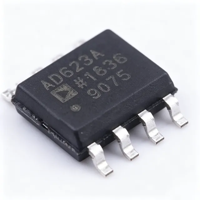
AD623ARZ-R7 - Rail-to-Rail In-Amp, 3-12V | Analog Devices
The Analog Devices AD623ARZ-R7 is a single-supply, rail-to-rail output instrumentation amplifier with a 2.7 V to 12 V supply range, 800 kHz bandwidth, and 90 dB minimum CMRR at G = 1, housed in an industry-standard 8-lead SOIC package (3.90 mm width). An instrumentation amplifier (in-amp) is a type of differential amplifier that amplifies the difference between two input signals while rejecting common-mode voltages. Characterized by high input impedance, high common-mode rejection ratio (CMRR), and low offset voltage, in-amps form a specialized subclass within the operational amplifier family and are essential building blocks in analog signal conditioning chains for precision sensing. Key features of the AD623ARZ-R7 include gain programming with a single external resistor via the formula G = 1 + 100 kOhm/RG (unity gain with no external resistor), rail-to-rail output swing, and input common-mode range extending 150 mV below ground on a single supply. It operates from single supplies of 3 V to 12 V or dual supplies of +/-2.5 V to +/-6 V, suiting both portable and industrial systems. Technically, the AD623 uses a classic three-op-amp topology with a laser-trimmed internal precision resistor network. The input stage provides high impedance and excellent CMRR, while the output stage delivers rail-to-rail swing. The REF terminal allows low-impedance level shifting of the output, critical for centering signals in single-supply data acquisition systems. A and B grades differ in offset voltage and drift specifications. Typical applications include load cell and pressure sensor signal conditioning, medical ECG front ends, thermocouple amplification, and industrial process control, where the high CMRR rejects common-mode noise in electrically noisy environments. When designing, place the gain resistor close to the device, bypass each supply pin with 0.1 uF, and drive the REF pin from a low-impedance source to preserve CMRR. This page synthesizes distributor pricing, drop-in alternatives, and practical design notes not found in the manufacturer datasheet.
AD629ARZ-R7 - ±270V Common-Mode Diff Amp SOIC-8 | ADI
The Analog Devices AD629ARZ-R7 is a precision difference amplifier rated for ±270 V common-mode input voltage in an 8-pin SOIC (R-7 tape & reel) package. It delivers 86 dB minimum DC CMRR, 1 V/V fixed unity gain, and 2.1 V/µs slew rate from a ±2.5 V to ±18 V dual supply. The device is an improved pin-for-pin replacement for the legacy INA117P and INA117KU. A difference amplifier is a specialized op-amp topology that subtracts two input signals and rejects the common-mode voltage present on both inputs. In the broader IC taxonomy it belongs to the instrumentation amplifier family (in-amp -> difference amplifier -> operational amplifier -> analog IC -> semiconductor). The AD629 specifically targets high common-mode industrial environments where signal levels up to ±270 V must be rejected to extract a small differential signal sitting on top of a large DC bus. Key features include ±270 V continuous common-mode range, 86 dB minimum CMRR (DC to 1 kHz), 500 kHz small-signal bandwidth, 2.1 V/µs slew rate, and integrated precision resistor networks that set unity gain without external components. The internal laser-trimmed thin-film resistors achieve 0.03% typical gain accuracy and excellent common-mode rejection over temperature. The AD629 uses a three-op-amp topology with input overvoltage protection through internal resistors and ESD clamps. Its supply current of approximately 1 mA (per amplifier, single gain stage active) keeps self-heating low, while the SOIC-8 (θJA = 155 °C/W) package is rated for -40 °C to +85 °C operation. Typical applications include motor control phase current sensing, 48 V/24 V battery monitoring, shunt-based high-side current measurement, industrial PLC analog front ends, and power inverter feedback. Designers choose it when they need to digitize a small differential signal riding on a high-voltage DC bus. Designers should ground both REF pins (1 and 5) to a low-impedance ground plane and leave pin 8 floating (NC). Using separate ground returns for input signal ground and REF ground degrades CMRR by tens of dB. This page synthesizes distributor pricing, drop-in alternatives, and PCB layout guidance not available from the manufacturer datasheet alone.
AD632SH/883B - Precision 4-Quadrant Multiplier | Analog Devices
The AD632SH/883B is an internally trimmed precision monolithic four-quadrant analog multiplier/divider from Analog Devices, packaged in a hermetic TO-100-10 metal can. It is pin-for-pin compatible with the industry-standard AD532 but offers improved specifications, including a fully differential high-impedance Z-input. The device can provide gains up to ×10, often eliminating the need for separate instrumentation amplifiers to precondition inputs. It operates over the military temperature range of -55°C to +125°C and is available in a through-hole TO-100-10 package. An analog multiplier is a circuit that produces an output voltage proportional to the product of two input voltages. The AD632 is a four-quadrant multiplier, meaning it can handle both positive and negative input signals, enabling applications such as modulation, demodulation, automatic gain control, and power measurement. As a precision analog computational building block, it sits within the broader category of analog signal processing ICs, which are essential in instrumentation, control systems, and communication equipment. Key features include excellent long-term stability, low noise, and high reliability. The device is internally trimmed for accuracy, reducing the need for external calibration. The fully differential Z-input allows flexible signal conditioning, and the ability to achieve gains up to ×10 simplifies system design. The TO-100-10 metal can package provides hermetic sealing, making it suitable for harsh environments. Technically, the AD632 uses a monolithic bipolar process with laser-trimmed thin-film resistors to achieve high accuracy. The transfer function is W = (X1 - X2)(Y1 - Y2)/10V + Z, where Z is the differential Z-input. This architecture supports multiplication, division, squaring, and square-rooting functions. The device is designed for precision analog computation, with a typical nonlinearity of ±0.5% and a small-signal bandwidth of 1 MHz. Typical applications include analog computation in test and measurement equipment, precision power measurement, process control, and signal conditioning in military and aerospace systems. The AD632SH/883B is particularly suited for applications requiring high accuracy and stability over a wide temperature range. When designing with this device, ensure proper power supply decoupling with 0.1 µF ceramic capacitors close to the supply pins. The output can drive loads down to 2 kΩ, and the Z-input can be used for offset adjustment or to sum signals. For division mode, the Y-input must be positive to avoid instability.

AD640TE/883B - 120MHz Log Amp, 50dB Range | Analog Devices
The AD640TE/883B is a complete monolithic logarithmic amplifier from Analog Devices, designed for high-frequency signal processing applications. It provides up to 50 dB of dynamic range for frequencies from DC to 120 MHz, making it ideal for RF power measurement, signal level detection, and wideband receiver systems. The device operates over the military temperature range of -55°C to +125°C and is available in a 20-lead ceramic leadless chip carrier (CLCC) package. A logarithmic amplifier is a specialized amplifier that produces an output voltage or current proportional to the logarithm of the input signal amplitude. This allows a wide dynamic range of input signals to be compressed into a manageable output range, which is essential in applications such as radar, communications, and test equipment where signal levels can vary by several orders of magnitude. The AD640 uses a successive detection scheme to achieve its logarithmic response, providing an output current that is proportional to the logarithm of the input signal. Key features of the AD640TE/883B include a 50 dB dynamic range, DC to 120 MHz bandwidth, and a successive detection architecture that ensures accurate logarithmic conversion. The device is specified for the military temperature range, making it suitable for defense and aerospace applications. The 20-CLCC package provides a compact, hermetically sealed solution that is resistant to harsh environmental conditions. The AD640TE/883B is processed to MIL-STD-883B, ensuring high reliability and compliance with military standards. This makes it a preferred choice for mission-critical systems where failure is not an option. The device's wide bandwidth and high dynamic range also make it suitable for use in instrumentation, where precise signal level measurement is required. Typical applications include RF power amplifiers, radar systems, communication receivers, and test and measurement equipment. The AD640TE/883B can be used in cascade to achieve up to 95 dB of dynamic range at reduced bandwidth, providing flexibility for applications requiring even greater dynamic range. When designing with the AD640TE/883B, it is important to consider the output current characteristics and the need for proper termination to achieve the desired logarithmic response. The device requires a single supply voltage and can be easily integrated into existing designs.
AD647SE/883B - Ultralow Drift Dual JFET Op Amp | Analog Devices
The AD647SE/883B is an ultralow drift, dual JFET operational amplifier from Analog Devices, designed for high-precision instrumentation and military/aerospace applications. It combines two matched JFET input amplifiers in a single hermetically sealed 20-lead ceramic leadless chip carrier (CLCC) package, processed to MIL-STD-883B for enhanced reliability. The device features a maximum input offset voltage of 500 µV, a low input bias current of 10 pA, and a minimum slew rate of 2 V/µs, making it suitable for precision signal conditioning. An operational amplifier (op amp) is a high-gain voltage amplifier with differential inputs and a single-ended output, used in analog signal processing. The AD647SE/883B is a dual op amp, meaning it contains two independent amplifiers in one package, saving board space and improving thermal tracking. As a JFET-input op amp, it offers very high input impedance and low bias current, ideal for interfacing with high-impedance sensors and precision integrators. Key features include ultralow drift (typically 0.5 µV/°C), low noise, and high common-mode rejection. The device operates from dual supplies up to ±18 V, with a nominal supply voltage of 15 V. The extended temperature grade (S) supports operation from -55°C to +125°C, meeting military temperature requirements. The 20-lead CLCC package provides a compact, hermetic solution for harsh environments. Technically, the AD647 uses ion-implantation and laser wafer drift trimming to achieve matched JFETs on a monolithic bipolar chip, resulting in superior DC precision. The device's bipolar technology ensures low offset voltage and drift, while the JFET input stage provides high input impedance. This combination makes it a versatile choice for precision analog circuits. Typical applications include precision instrumentation amplifiers, active filters, data acquisition systems, and military avionics. Its low drift and high accuracy are critical in these applications where temperature variations can degrade performance. When designing with the AD647SE/883B, ensure proper decoupling of the power supply pins with 0.1 µF ceramic capacitors close to the device. Also, consider the input bias current and offset voltage when designing high-impedance circuits, and use appropriate guarding techniques to minimize leakage currents.