دوائر المضخم المتكاملة
المنتجات (1,100+)

MC1458IN - Dual High-Performance Op Amp | STMicroelectronics
STMicroelectronics MC1458IN is a dual, high-performance, general-purpose operational amplifier packaged in an 8-pin Mini DIP. Each integrated circuit contains two amplifier channels, allowing one component to implement independent amplification, buffering, summing, integration, or feedback functions. The device is specified as a standard general-purpose amplifier, and a distributor listing identifies a slew rate of 0.8 V/µs. It is supplied in the through-hole DIP-8 package represented by the MC1458IN ordering code. An operational amplifier, or op amp, is a high-gain analog building block that compares its inverting and non-inverting inputs and drives an output toward the difference between those voltages, subject to negative feedback. Within the product hierarchy, the MC1458IN is a dual op amp, which is a type of analog amplifier IC used for instrumentation, signal conditioning, voltage following, active filtering, summing, and feedback control. The MC1458 family provides two amplifiers in one monolithic package, reducing component count while preserving independent operation of both channels. Key features include two amplifier circuits in one package, a high-performance monolithic design, general-purpose feedback compatibility, a stated 0.8 V/µs slew rate, and an 8-pin Mini-DIP mounting format. These characteristics make the device suitable for analog systems requiring two precision-oriented signal paths without allocating two separate single amplifier packages. The through-hole package also supports conventional DIP sockets and prototype-board assembly. According to the STMicroelectronics manufacturer datasheet, the MC1458 is intended for a wide range of analog applications, including integrators, summing amplifiers, and general feedback circuits. Its high gain and broad operating-voltage capability support conventional closed-loop analog designs, while the integrated dual configuration allows signal conditioning and active feedback stages to be placed close together on a board. Typical applications include audio preamplification, instrumentation stages, active filters, analog summing networks, integrators, buffer amplifiers, and general industrial signal conditioning. In a dual-rail circuit, the two channels can process separate inputs or participate in cascaded stages. In single-supply equipment, the usable input and output range still requires careful common-mode and output-swing verification against the manufacturer specifications. Designers should check the datasheet pinout, recommended operating voltages, common-mode range, output swing, offset specifications, compensation requirements, and supply decoupling before finalizing a board. Feedback-network values and source impedances should be selected against the documented frequency-response and noise characteristics rather than estimated from generic 741-family behavior. This page consolidates verified manufacturer and distributor information, documented equivalent-family references, package-level comparison data, and practical selection guidance. It also distinguishes verified facts from parameters that still require confirmation from the current manufacturer datasheet, helping engineers qualify replacements without assuming undocumented electrical equivalence.

MC1458PS - Dual 30V 1MHz Op Amp | Texas Instruments
The Texas Instruments MC1458PS is a dual general-purpose operational amplifier with two internally compensated amplifier channels, a 30 V rating, and a 1 MHz gain-bandwidth product in an 8-pin SOIC package. The MC1458 family combines short-circuit protection, wide common-mode and differential input-voltage ranges, low power consumption, and latch-up-free operation. An operational amplifier is an analog integrated circuit that uses high-gain differential amplification to compare and amplify small voltage differences. The MC1458 belongs to the general-purpose operational-amplifier family within the broader analog IC and semiconductor hierarchy. Its two channels can operate independently for signal conditioning, voltage following, summing, integration, or other feedback-based amplifier configurations. Each MC1458 channel offers a 1 MHz gain-bandwidth product, 500 V/ms slew rate, and 90 dB common-mode rejection in the supplied product data. The reported input bias current is 1.5 µA, input offset current is 200 nA, and typical input offset voltage is 6 mV. Internal frequency compensation eliminates the need for external compensation components in the manufacturer's standard voltage-follower application. The MC1458 architecture is intended for general-purpose precision amplification rather than high-speed or rail-to-rail operation. Its wide common-mode input range makes it suitable for conventional bipolar-supply circuits, while the absence of latch-up improves robustness during power sequencing and input-overvoltage events. Short-circuit protection helps limit output current when an output is overloaded, although sustained short-circuit duration and internal current limits should be confirmed in the manufacturer datasheet. Typical uses include audio preamplification, summing amplifiers, active filters, sensor-signal conditioning, industrial control blocks, and general voltage-following circuits. Two amplifiers in one package can reduce component count and simplify dual-channel or differential signal-path layouts. The commercial MC1458PS temperature grade is 0 °C to +70 °C, making it appropriate for room-temperature industrial and consumer equipment rather than exposed automotive or extreme-temperature installations. PCB design should reserve adequate copper around the supply pins and route each channel's feedback components close to the associated amplifier pins to reduce parasitic feedback and instability. Decoupling capacitors should be placed directly between each supply pin and ground. Because this is a non-rail-to-rail, bipolar general-purpose amplifier, input and output common-mode headroom must be checked against the actual supply voltages. This page combines verified manufacturer and distributor information, drop-in family alternatives, package and pinout details, application guidance, and design notes to provide more implementation context than the basic distributor catalog entry.

MC3302P - Quad Single-Supply Comparator | onsemi
The onsemi MC3302P is a quad single-supply comparator with a 14-pin PDIP package. It provides four independent comparator channels for level detection, low-level sensing, memory applications, and other consumer, automotive, and industrial electronics systems. The verified product data identifies a typical input bias current of 25 nA and a typical input offset current of ±5.0 nA, while the specified comparison capability covers ±15 V and 30 V operation. Its through-hole PDIP-14 construction supports legacy industrial and automotive circuit boards that were designed around a quad comparator rather than a newer surface-mount package. A comparator is an analog integrated circuit that compares two input voltages and produces a logic-level output indicating which input is higher. The MC3302P belongs to the comparator hierarchy, which also includes voltage comparators and differential amplifiers used in control and signal-conditioning systems. As a single-supply device, it is intended for systems where the comparator must operate from one supply rail while detecting small voltage differences within that rail. The MC3302P's four channels provide practical space savings compared with four discrete comparators. Its typical 25 nA input bias current minimizes loading on high-impedance sensing nodes, while the typical ±5.0 nA input offset current supports accurate threshold decisions near the reference voltage. The device is suited to console, automotive, and industrial applications where level detection and low-level sensing must be implemented with a familiar 14-pin through-hole footprint. Each channel compares an inverting and a non-inverting input and provides an open-collector output, allowing the outputs to be pulled up as required by the host logic and to support wired logic when several outputs are combined. The open-collector architecture provides design flexibility but requires an external pull-up resistor. The output transistor can sink current when the comparator condition is met, while the pull-up establishes the inactive high voltage. Typical uses include battery threshold detection, sensor signal conditioning, window or level comparison, memory-control interfaces, and industrial control modules. Because this is a legacy-style PDIP device, it is especially relevant to maintenance of existing equipment rather than new space-constrained designs. Designers should confirm the exact pinout and output truth table against the manufacturer documentation before modifying an existing board. The principal design consideration is supply bypassing. Place the required decoupling capacitor close to the device supply pins and return each comparator input directly to its pin rather than routing it through shared analog traces. Account for input offset and bias currents when setting very small thresholds, and use a pull-up resistor compatible with the required output rise time and available sink current. This product record combines verified manufacturer and distributor information with package, application, design, and replacement guidance. It also distinguishes exact technical data from values that require confirmation, helping engineers source MC3302P parts without treating unsupported compatibility or price claims as verified facts.

MC3303DG - 4-Channel 1 MHz Op Amp | onsemi | 14-SOIC
The onsemi MC3303DG is a four-channel general-purpose operational amplifier with true differential inputs, 1 MHz gain-bandwidth product, and 0.6 V/us slew rate, housed in a 14-pin SOIC package. Designed for single-supply operation from 3 V to 36 V, the device also supports split-supply operation, making it suitable for industrial control, instrumentation, sensor conditioning, and general analog signal-processing systems. Each amplifier includes internal frequency compensation, low input bias current, and short-circuit protection, allowing stable operation without external compensation networks in typical closed-loop configurations. An operational amplifier is an analog integrated circuit that amplifies the voltage difference between its inverting and non-inverting inputs. In the product taxonomy, the MC3303DG belongs to the operational-amplifier and instrumentation-amplifier hierarchy, then to the broader amplifier IC and semiconductor categories. Its internally compensated architecture simplifies design by fixing the gain-bandwidth relationship while preserving a practical combination of supply flexibility, low power consumption, and general-purpose functionality. The principal electrical features include four independent amplifiers, 1 MHz gain-bandwidth product, 0.6 V/us slew rate, and 8 mV input offset voltage as listed for the industrial-temperature version. The device operates from 3 V to 36 V under a single supply, while dual-supply operation remains possible when the total supply span is adequate. A class AB output stage supports practical drive into typical feedback networks, and true differential inputs help reject common-mode signals when both inputs are biased within the common-mode range. The MC3303 architecture is intended as a cost-conscious alternative to the uA741-class quad amplifier while adding advantages for modern single-supply systems. Internal frequency compensation removes the need for a dominant-pole compensation capacitor in most closed-loop applications. Designers must still account for output swing, input common-mode range, bias current, noise, stability, and supply bypassing when using the amplifier in precision or high-frequency circuits. Typical applications include industrial control loops, transducer and sensor signal conditioning, audio preamplification, analog measurement front ends, power-supply feedback networks, and low-frequency communications equipment. Four amplifiers in one package can reduce board area in designs requiring multiple independent analog channels, although common supply routing and decoupling remain critical. The most important design practice is to place input, output, and bypass connections for short, low-impedance paths while keeping sensitive input traces away from power outputs and switching nodes. Verify the exact input and output voltage limits, bias-current behavior, load capability, and noise specifications against the manufacturer datasheet before finalizing a precision application. This page consolidates verified distributor information, package-specific alternatives, technical comparisons, and practical design guidance for engineers evaluating the MC3303DG. It emphasizes what is confirmed from supplied sources and explicitly marks unavailable electrical details rather than estimating them, supporting more reliable procurement and design decisions.
MC3303DT - 1MHz Low-Power Quad Op Amp | STMicroelectronics
STMicroelectronics MC3303DT is a low-power, quad bipolar operational amplifier featuring four amplifiers, true differential inputs, internally compensated operation, and a 1 MHz gain-bandwidth product. The device operates from single +3 V to +36 V supplies or from dual ±18 V supplies and is packaged in a 14-pin SOIC. Each amplifier is designed for general-purpose signal conditioning using its Class AB output stage and short-circuit-protected outputs. An operational amplifier is a voltage-gain element that compares its inverting and non-inverting inputs and drives its output toward a voltage representing the difference between them. The quad configuration belongs to the operational-amplifier family within analog integrated circuits and amplifier ICs. MC3303DT provides four independent amplifiers in one package, reducing board area compared with four single or dual amplifier packages when a system requires four similar signal-processing channels. The principal features include a 1 MHz gain-bandwidth product, operation from 3 V to 36 V, low input bias current of 500 nA maximum, internal frequency compensation, and short-circuit-protected outputs. Its Class AB output stage is intended to provide a practical compromise between output drive capability and power dissipation compared with a pure Class A stage. The low-power operating point makes the device suitable for industrial control, instrumentation, sensor interfaces, and general analog signal-conditioning systems. MC3303DT differs from the closely related UA741-family architecture through its improved suitability for single-supply operation. It accepts a positive supply as high as 36 V or dual supplies of ±18 V, allowing operation from industrial 24 V rails when the total supply and input/output signal limits are observed. Internally compensated amplifiers simplify closed-loop gain selections when unity-gain stability is appropriate for the selected circuit and load. Typical uses include four-channel sensor amplification, differential input conditioning, active filtering, comparator-style threshold functions, and general instrumentation. The four amplifiers may also process separate channels or be combined in wider-bandwidth or higher-gain configurations where the resulting feedback network remains stable. Designers should account for input common-mode range, output swing, noise, and load capability at their intended supply voltage. A key design consideration is power: each amplifier contributes to total quiescent current, so four channels require more supply current than one or two channels. Input and output stability should be verified with the intended source impedance, load, supply decoupling, and feedback network. Input and output pin functions are published in the manufacturer datasheet, which should be checked against the final 14-pin PCB footprint. This page combines verified distributor data, manufacturer-document references, application guidance, package details, and same-footprint replacement considerations. It also identifies where current sourcing information remains unavailable so engineers can distinguish documented facts from data requiring confirmation before production release.
MC3303N - Quad 30V 1MHz Op Amp | Texas Instruments
The Texas Instruments MC3303N is a quad, low-power bipolar operational amplifier specified for a 30 V maximum supply and 1 MHz unity-gain bandwidth, housed in a 14-pin PDIP package. It provides four amplifiers in one package for general-purpose signal conditioning, transducer interfaces, analog summing, filtering, and feedback-control circuits. An operational amplifier is a voltage-amplified differential-input device whose external feedback network determines its behavior. MC3303 belongs to the operational-amplifier hierarchy: quad low-power op amp, bipolar linear amplifier, analog signal-conditioning IC, and semiconductor. Four independent amplifiers in one 14-pin package reduce board area compared with four separate single or dual amplifier packages, although users must preserve adequate spacing and decoupling for stable low-noise operation. Verified manufacturer information identifies the MC3303N as a standard general-purpose four-circuit amplifier in a 14-pin PDIP package, with a 30 V supply rating and 1 MHz gain-bandwidth product. The family is intended for single-supply or split-supply operation when the electrical limits specified by the manufacturer are met. Because the target uses a through-hole PDIP package, it also supports prototype repair and conventional leaded-board assembly rather than requiring a fine-pitch SMT footprint. The integrated amplifier count makes the device useful when a board needs multiple similar signal paths. Typical uses include four sensor channels, four analog-control loops, dual-channel buffering with spare amplifier capacity, or small active-filter sections. Designers should check common-mode range, output swing, input bias behavior, supply current, noise, slew rate, stability, and temperature limits against the manufacturer datasheet before fixing the operating conditions. The MC3303N should be placed near the supported decoupling network, with power and ground return paths arranged to minimize resistance and switching noise. Input and feedback components should be positioned to reduce parasitic capacitance at the high-frequency nodes. Do not infer exact bias-current, noise, slew-rate, common-mode, or temperature values from the search summaries; those parameters require the official manufacturer datasheet before release to production. This page combines verified product identity, source links, package information, application guidance, and explicitly marked data gaps. The comparison section is limited to candidates that the provided evidence supports as MC3303N equivalents; any claimed drop-in substitution must still be checked against pin assignment, electrical limits, supply requirements, and the intended operating conditions.
MC33077P - 37 MHz Low-Noise Dual Op Amp | onsemi
The onsemi MC33077P is a dual, general-purpose operational amplifier built with precision bipolar design techniques, providing a 37 MHz gain-bandwidth product and an 11 V/µs slew rate in an 8-pin PDIP package. It is intended for instrumentation, signal-conditioning, and amplification applications that require low noise, high frequency response, and precise channel matching. An operational amplifier, or op amp, is an analog active device that amplifies the difference between two input voltages. The MC33077P contains two independent amplifier circuits in one monolithic package, making it a dual op amp. Within the product hierarchy, it belongs to the operational amplifier and analog amplifier categories, where it provides a higher-speed alternative to general-purpose precision amplifiers. The MC33077 family uses innovative bipolar construction, analog resistor trimming, and dual-doublet frequency compensation. Analog trimming is used to obtain low input offset voltages, while the precision-matching approach supports closely matched amplifier channels. These techniques support applications in measurement systems, audio and communication circuits, active filters, and low-level analog signal chains. Verified distributor information identifies the MC33077P as a 2-circuit, 8-PDIP general-purpose amplifier with 37 MHz bandwidth. A separate distributor listing reports an 11 V/µs slew rate, indicating that the device can support signal transitions well beyond audio frequencies when the surrounding circuit permits. Exact noise density, input bias current, input offset voltage, supply-current, and common-mode limits were not included in the supplied verification data and must be confirmed against the manufacturer datasheet before design release. Typical uses include instrumentation preamplification, active filtering, audio signal conditioning, and general high-frequency analog processing. In a typical signal chain, the device would follow a low-amplitude sensor or filter stage and drive a higher-impedance ADC input, buffer, or measurement front end. Because the amplifiers are internally matched, dual-channel differential or ratiometric measurements are practical when board layout and resistor matching are controlled. The primary design consideration is ensuring that the surrounding circuit does not degrade the amplifier's noise and accuracy performance. Place decoupling capacitors close to the supply pins, keep feedback-loop routing short, and avoid parasitic capacitance on high-impedance input nodes. Confirm the exact pinout, supply range, noise specifications, input common-mode limits, and output-current capability in the onsemi MC33077 datasheet before layout release.
MC33078P - Dual 16MHz Low-Noise Op Amp | Texas Instruments
The Texas Instruments MC33078P is a bipolar dual operational amplifier with 16 MHz gain-bandwidth product, a 7 V/µs slew rate, and 4.5 nV/√Hz input voltage noise, supplied in an 8-pin PDIP package. The device supports single-supply and dual-supply operation over a voltage range of ±5 V to ±18 V and is intended for quality audio and data-signal processing applications. An operational amplifier is an analog signal-conditioning IC that uses high-gain differential amplification to increase the voltage difference between two inputs. In the wider hierarchy, an op amp belongs to amplifiers, analog integrated circuits, and signal-chain conditioning devices. The MC33078P contains two independent amplifiers in one package, allowing one package to serve two channels while reducing board area and simplifying dual-audio or dual-data-signal designs. The MC33078/9 family uses bipolar transistor technology with high-frequency PNP input transistors. This architecture provides low input voltage noise, high gain-bandwidth product, high slew rate, low total harmonic distortion of 0.002%, and a low input offset voltage of 0.15 mV. These characteristics make the amplifier suitable for audio preamplification, filtering, instrumentation, and general-purpose analog signal conditioning where both small-signal fidelity and bandwidth are important. The two channels operate independently from the same supply pins. Its 16 MHz gain-bandwidth product allows useful closed-loop bandwidth well below the unity-gain frequency, while the 7 V/µs slew rate supports faster large-signal transitions than many general-purpose bipolar op amps. Noise and distortion figures should therefore be evaluated in the same signal bandwidth and output amplitude used in the target circuit; headline values do not describe complete system performance by themselves. Typical uses include microphone and line-level audio amplification, active filters, analog instrumentation, low-level sensor conditioning, and dual-channel signal processing. The 8-pin PDIP package is suitable for through-hole construction, prototyping, repair work, and applications where the larger package is acceptable. Local bypass capacitors close to the supply pins remain important for stable operation and low-noise performance. The principal design trade-off is package size rather than electrical capability: PDIP-8 is easy to install manually but occupies more PCB area than surface-mount dual-op-amp packages. Designers should preserve adequate output-current headroom for capacitive loads, verify stable operation with the selected feedback network and load, and avoid assuming that low-noise input devices are interchangeable with FET-input amplifiers because bias-current and distortion behavior differ. This page consolidates the verified manufacturer specifications, distributor availability references, and engineering-focused selection guidance for MC33078P. It also distinguishes documented MC33078-family options from true pin-compatible replacements, helping engineers avoid treating merely similar amplifiers as drop-in substitutes.
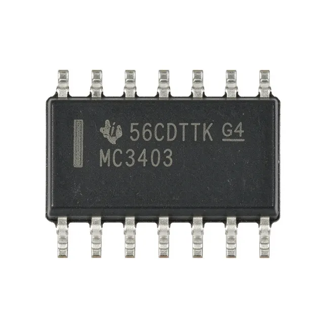
MC3403D - Quad 30 V 1 MHz Op Amp | Texas Instruments
The Texas Instruments MC3403D is a quad, general-purpose bipolar operational amplifier built for single-supply and dual-supply analog systems. The device provides four amplifiers in a 14-SOIC package, operates from ±2.5 V to ±15 V according to the cited distributor specification, and supports a 1 MHz gain-bandwidth product. Its four-circuit integration reduces package count while providing true differential inputs and push-pull output capability. What is a quad operational amplifier? A quad operational amplifier combines four independent amplifier sections in one IC. These amplifiers serve as the active gain elements in sensors, buffers, analog filters, comparators, and feedback-control circuits. The MC3403 belongs to the operational-amplifier hierarchy, which is part of the broader amplifier-IC and signal-conditioning categories used in industrial control, instrumentation, audio, and communications equipment. Key verified features include four amplifier circuits, 1 MHz operation, 0.6 V/µs slew rate, a 14-pin SOIC package, and operation from −25 °C to 85 °C. The push-pull output stage supports bidirectional output-current drive in suitable loads, while the quad configuration gives designers four reusable analog channels in one package. These attributes make the MC3403D practical for low-to-moderate-frequency analog signal paths where four similar amplifier functions are required. The MC3403’s electrical characteristics are described as similar to the popular UA741 family, but its architecture is specifically useful in single-supply applications. Compared with a basic dual-supply-only op amp, the part offers a practical path to operating from a single rail in many circuits. Designers must still check input common-mode limits, output swing, supply current, noise, offset behavior, and stability against the manufacturer datasheet for the exact operating condition. Typical uses include sensor buffering, low-frequency active filtering, audio preamplification, transducers, analog control loops, and general instrumentation. For a new design, confirm the required input and output voltage ranges, acceptable slew rate, load impedance, noise performance, and temperature limits. For a replacement, verify the exact pinout, supply range, common-mode range, and output-swing requirements rather than relying only on the amplifier count. A key practical consideration is decoupling. Place the required supply bypass capacitors close to the power pins and keep sensitive input and feedback traces short. The MC3403D is a general-purpose amplifier, not a precision or high-speed device; use a more specialized amplifier when low offset, low noise, high speed, rail-to-rail operation, or extended temperature performance is mandatory. This page consolidates verified manufacturer and distributor information, drop-in alternatives, application guidance, package details, and selection considerations for engineers evaluating MC3403D. It is intended to support procurement and design review without substituting unsupported specifications for missing datasheet data.
MC3403DG - Quad 1MHz Op Amp, 3-36V | onsemi
onsemi MC3403DG is a quad general-purpose operational amplifier with true differential inputs, a 3 V to 36 V supply range, 1 MHz gain-bandwidth product, and a 14-pin SOIC package. It provides four amplifiers in one package and is designed for single-supply signal-conditioning, buffering, filtering, current-sensing, analog measurement, and precision-control circuits. An operational amplifier, or op amp, is a voltage-amplified differential building block whose open-loop gain falls with frequency. The MC3403 family belongs to the broader hierarchy of analog amplifier ICs used to amplify small differential signals, buffer high-impedance sources, implement active filters, and close feedback loops around sensors or actuators. Its true differential inputs make the device particularly useful when a useful output must follow the difference between two input voltages rather than either input alone. The quad configuration provides four amplifiers in one 14-pin SOIC, reducing board area and simplifying multi-channel designs. Key characteristics include operation from 3 V to 36 V, a 1 MHz gain-bandwidth product, and a maximum input offset voltage of 10 mV as listed by Mouser. The part is identified as a standard general-purpose amplifier and is suitable for instrumentation, buffer-amplifier, measurement, filtering, and precision-control applications. Its single-supply capability is particularly useful in cost-sensitive systems where one supply rail must support the complete analog signal chain. Differential inputs allow subtraction, current-loop monitoring, sensing across resistive elements, and amplification of sensor outputs without external input networks. Because the package contains four amplifiers, designers can use matched functional channels for simultaneous acquisition, multi-axis sensing, or multiple filter stages while preserving consistent board organization. Typical uses include 4-20 mA process-control inputs, resistive sensor conditioning, active low-pass or band-pass filters, buffered sensor outputs, general-purpose instrumentation, and current-shunt measurements. The 3 V minimum supply supports modern 3.3 V systems, while the 36 V maximum provides additional headroom for industrial supply rails. Commercial-temperature operation is identified in distributor listings, although the exact temperature limits require confirmation from the manufacturer datasheet. When laying out a MC3403DG circuit, place input, feedback, and compensation components close to the relevant SOIC pins and provide adequate return paths for each amplifier channel. Decoupling capacitors should connect between the supply pins and ground with short traces, and unused amplifier inputs should be tied to a defined potential rather than left floating. Check output-current, input-common-mode, noise, and stability requirements against the complete operating conditions before finalizing the design. This product page combines verified manufacturer and distributor information, a complete 14-pin pinout, practical single-supply design guidance, and a parameter-based comparison with available 14-pin quad amplifier alternatives. It also distinguishes confirmed electrical characteristics from parameters that still require verification in the manufacturer datasheet.
MC3403N - Quad 30V 1MHz Op Amp | Texas Instruments
The Texas Instruments MC3403N is a quad general-purpose operational amplifier built for single- and dual-supply systems, with four amplifiers, a 30 V maximum supply rating, 1 MHz typical gain-bandwidth product, and operation from -25°C to 85°C. It is supplied in a 14-pin PDIP package. An operational amplifier is an analog integrated circuit that uses high-gain differential feedback to amplify the difference between two input voltages. The MC3403 belongs to the broader amplifier hierarchy: operational amplifier, analog IC, semiconductor, and general-purpose signal-conditioning component. Its quad construction reduces package count when a design needs several independent gain stages, buffers, or comparators. The verified product information identifies wide supply-voltage support, a true differential input stage, internal frequency compensation, low input bias current, a Class AB output stage, and short-circuit protection. The 1 MHz gain-bandwidth product is suitable for general-purpose audio, control, and instrumentation circuits rather than precision or high-speed applications. Because all four amplifiers share one package, supply pins and exposed signal pins must be routed carefully on mixed analog and digital boards. The 30 V supply capability permits operation from conventional single supplies or split dual supplies, making the device useful in legacy industrial, audio, and control designs. However, exact input common-mode limits, output swing, input offset voltage, supply-current, noise, and slew-rate values are not stated in the supplied verified excerpts; those parameters require confirmation in the manufacturer datasheet before final circuit sign-off. Typical applications include four-channel audio preamplification, low-frequency active filtering, sensor-signal conditioning, industrial control loops, and general buffer or gain stages. In each case, the 1 MHz bandwidth should be compared with the closed-loop gain and required settling behavior. A four-amplifier package can reduce board area, but it does not eliminate the need to check common-mode range, output swing, stability, and supply-decoupling requirements at every amplifier section. Design with a local bypass capacitor near the supply pins, maintain the required input common-mode range, and verify output-voltage headroom under the intended load. Do not infer precision performance from the word general-purpose. This product page consolidates the verified manufacturer identity, distributor listing, package, temperature range, supply rating, and replacement research while explicitly marking unavailable detailed electrical parameters. The alternatives listed here are limited to candidates supported by the supplied cross-reference data and are presented as package-compatible engineering options; final qualification should confirm pinout, supply limits, input/output ranges, offset, bandwidth, slew rate, and lifecycle status against the selected manufacturer datasheet.
MC34071D - 44V Single-Supply Operational Amplifier | onsemi
The onsemi MC34071D is a single-supply operational amplifier designed for operation from 3.0 V to 44 V, with a 4.5 MHz gain-bandwidth product and a 13 V/µs slew rate. The device is packaged in an 8-pin SOIC and uses bipolar fabrication rather than JFET input devices. Its combination of high bandwidth, fast slew rate, and a wide supply-voltage range makes it suitable for industrial instrumentation, signal conditioning, data acquisition, and control systems that operate from elevated supply voltages. An operational amplifier is a high-gain differential amplifier used to amplify small input signals, buffer sensors, drive analog stages, and implement feedback-control networks. The MC34071 belongs to the broader hierarchy of operational amplifier, analog amplifier, signal-conditioning IC, and semiconductor. Although the MC34071 family can operate from split supplies, it is particularly suited to single-supply operation, which simplifies circuits whose signal reference is close to the lower supply rail. The family provides 4.5 MHz of gain-bandwidth product, a 13 V/µs slew rate, and fast settling time without using JFET device technology. The specified single-supply performance is defined at 5.0 V. The amplifiers are also functional at 3.0 V at 25°C, although bandwidth, slew rate, DC gain, and other parameters may change in that operating region. This distinction is important when designing at the minimum supply voltage. The bipolar process supports operation from a single 5.0 V supply or higher while accommodating input and output signals referenced toward ground. The wide 44 V maximum supply rating provides additional operating headroom for industrial systems while retaining the usual bipolar advantages of low input-voltage noise and accurate behavior around the output operating point. Designers should still use the manufacturer datasheet limits for input common-mode range, output swing, supply current, and stability with the selected gain and load. Typical uses include sensor-interface amplifiers, low-side current measurement, industrial control loops, audio and communications signal conditioning, active filtering, and general-purpose analog processing. Because the amplifier is optimized for single-supply operation, input and output signal levels must remain inside the datasheet common-mode and output-swing limits. Input common-mode limits depend on supply voltage and gain, so a signal that is valid at 5 V may not remain valid at 3 V. The main design consideration is supply headroom. Use decoupling close to the supply pins, verify that the selected feedback network remains stable at the intended noise gain, and check output-current capability for the load and output-voltage conditions. The MC34071 is not intended to replace a rail-to-rail input or output amplifier where signals exceed its specified common-mode or swing limits. This page combines verified manufacturer and distributor information with practical selection criteria, sourcing guidance, and verified same-package alternatives. It highlights where the MC34071D fits, where its non-rail-to-rail architecture requires careful signal-range review, and which replacement MPNs should be checked against the full datasheet before substitution.
MC34119D - Low-Power Class AB Audio Amplifier | NXP
The NXP MC34119D is a low-power, mono Class AB audio amplifier integrated circuit designed primarily for telephone equipment, including speakerphones. It operates from a 2 V minimum supply, supports a nominal range of 2 V to 16 V or ±1 V to ±8 V, and provides differential speaker outputs to increase usable output swing at low supply voltages. The device is supplied in an 8-pin SOIC package according to the distributor product listing. An audio amplifier is an integrated circuit that accepts a low-level analog audio signal and delivers enough current and voltage to drive a speaker or another acoustic transducer. The MC34119 belongs to the Class AB amplifier category, where the output transistors conduct during the signal cycle for improved efficiency than a continuously biased Class A design. Its telephone-oriented architecture supports portable and line-powered equipment where low supply voltage and compact implementation are important. The verified feature set includes a shutdown function, a single mono output channel, and differential speaker outputs. Differential outputs are particularly useful in telephone and speakerphone designs because they increase output swing into a differentially connected transducer. The manufacturer datasheet also identifies a 2.0 V minimum supply, allowing operation from low-energy source rails. The Class AB output stage is intended to balance output capability against power consumption in compact audio systems. MC34119D applications include telephone speakerphones, compact voice terminals, intercom equipment, and other low-voltage audio products. In these systems, the amplifier converts a microphone or line-level signal into a differential drive capable of energizing a small speaker. Designers should account for the external output-coupling capacitors shown in the manufacturer application circuit when connecting a speaker, and should verify the shutdown-control polarity and timing before sequencing the device. The most important design consideration is ensuring that the supply, input signal, output network, and speaker load remain within the limits defined by the manufacturer datasheet. Because the target is a legacy low-power audio amplifier, purchasing decisions should also account for lifecycle status, stock, and long-term sourcing rather than assuming availability from an active-production family. This page consolidates the verified package, supply-voltage, amplifier-class, shutdown, and differential-output information with practical selection guidance. It also distinguishes confirmed facts from parameters that require confirmation in the original MC34119 manufacturer datasheet, helping engineers evaluate MC34119D without relying on incomplete distributor summaries.
MC34119P - 2-16V Mono Class AB Audio Amp | NXP
NXP MC34119P is a low-power, 1-channel Class AB audio amplifier IC designed for telephone equipment, including speakerphones, with a 2 V to 16 V supply range and differential speaker outputs in an 8-pin DIP package. It provides a practical solution where low supply voltage, low quiescent current, and efficient single-speaker drive are required. The available ordering information identifies the device as an NXP USA Inc. 8-PDIP mono audio amplifier. An audio amplifier IC is a semiconductor that accepts a small audio signal and delivers enough voltage and current to drive a loudspeaker or other audio transducer. A Class AB amplifier combines the low crossover distortion of class-A operation with improved efficiency compared with a continuously biased class-A stage. In the MC34119P, differential speaker outputs are intended to maximize output swing at low supply voltages, making the device especially relevant to compact telephone and communications equipment. The MC34119P operates from 2.0 V to 16 V, as documented in the retrieved manufacturer and distributor information. Its typical quiescent supply current is 2.7 mA for battery-powered designs, while shutdown reduces the typical quiescent current to 65 µA. A chip-disable input provides a direct means of placing the amplifier in its low-power state. These features allow the amplifier to remain useful when system power is constrained by a telephone line or battery source. Its architecture uses one Class AB output channel and differential speaker outputs rather than a conventional single-ended output arrangement. Differential drive can provide greater useful voltage swing into the speaker for a given supply, which is important at the 2 V minimum supply. This is a system-level advantage in speakerphone products where loudness and battery efficiency must coexist. Exact continuous output power, output impedance, gain settings, and distortion limits were not included in the retrieved source snippets and must be confirmed in the full manufacturer datasheet before final design sign-off. Typical uses include telephone speakerphones, telephone-line powered communications products, small intercom stations, compact voice monitors, and portable low-voltage audio equipment. The device is also suitable where standby consumption matters, because the shutdown function can isolate the amplifier from the active signal path. For these applications, the 2 V minimum operating voltage and differential output capability align particularly well with low-power, single-speaker systems. The primary design consideration is output-device and load compatibility. Engineers should verify speaker impedance, output power at the available supply voltage, thermal conditions, gain configuration, bypass capacitors, and shutdown logic against the complete MC34119 datasheet. Because the supplied text identifies an 8-DIP footprint but does not enumerate individual terminal functions, the pin assignment and exposed circuit details should not be inferred solely from this page. This product page consolidates the verified MC34119P package, voltage, topology, shutdown, and low-power information with practical application guidance, sourcing considerations, and honest drop-in replacement analysis. Its key value is separating confirmed MC34119P characteristics from unverified specifications and avoiding unsupported claims about substitutes that may require different EMI performance or pin behavior.

MC3461L - Dual Current Sense Amplifier | Motorola | CDIP-16
The Motorola MC3461L is a dual current-sense amplifier in a 16-pin CDIP package, with two amplifier circuits for measuring current across low-value shunt resistors. The verified distributor data identifies the device as a high-speed NMOS/MECL current-sense amplifier, while detailed electrical limits, gain values, common-mode range, supply voltage, and temperature ratings are not included in the supplied records and therefore remain unconfirmed. Its instrumentation-amplifier classification places it among amplifier ICs used for power-conversion monitoring, motor control, battery management, and power-supply feedback. A current-sense amplifier is a specialized voltage-feedback amplifier that develops a measurable output voltage from the small differential voltage created by current flowing through a shunt resistor. The MC3461L contains two circuits, allowing one packaged device to monitor two independent current paths when the circuit board has sufficient isolation and the operating conditions of both channels are compatible. The 16-CDIP mechanical format is a through-hole ceramic dual in-line package intended for legacy industrial, instrumentation, and telecommunications equipment. The MC3461L's two-circuit architecture reduces component count compared with two separate single amplifiers, while its small shunt-generated differential signal supports compact sensing layouts. However, stable measurement depends on selecting an appropriate shunt, keeping Kelvin connections narrow and symmetrical, and observing the amplifier's common-mode and output limits. Because those numerical limits are absent from the verified excerpts, designers should consult the complete manufacturer datasheet before finalizing resistor values, gain configuration, supply rails, or production tolerances. The MC3461L is suitable for power-supply current monitoring, battery charge and discharge sensing, motor-control feedback, industrial process-control systems, and communications equipment. In these applications, the amplifier converts bidirectional or unidirectional shunt current into a voltage suitable for an ADC, controller, comparator, or protection circuit. The exact input polarity, output reference arrangement, and permissible common-mode voltage must be verified from the full datasheet before layout sign-off. A practical design begins by placing the shunt and amplifier in the same high-current path, routing the sense traces as a tightly coupled differential pair, and grounding the unused inputs or amplifier according to the manufacturer's recommended configuration. Decoupling capacitors should connect directly to the supply pins, and the output must remain within the device's verified output range. PCB creepage, clearance, copper heating, and Kelvin-trace geometry are as important as the IC choice in a high-current design. This page combines verified distributor identity and availability information with clearly marked engineering gaps, practical application context, and design guidance. It does not infer missing electrical specifications from the MC3461 family name, so procurement, electrical, and package decisions should be completed against the official datasheet and current authorized-channel inventory.
MC4558CP1 - Dual 2.5MHz Wide-Bandwidth Op-Amp DIP-8 | onsemi
The onsemi MC4558CP1 is a monolithic dual wide-bandwidth operational amplifier housed in an 8-pin PDIP (DIP-8) through-hole package, internally compensated and pin-compatible with the industry-standard 1458/4558 pinout. According to the onsemi datasheet, each of the two on-chip amplifiers delivers a unity-gain bandwidth of 2.5 MHz (C-grade) and 2.0 MHz (AC-grade), with the MC4558AC variant specifically guaranteed to the 2.5 MHz figure. The device targets cost-sensitive general-purpose analog signal-conditioning roles that benefit from higher small-signal bandwidth than the legacy 1458 family. What is an operational amplifier (op-amp)? An op-amp is a high-gain DC-coupled differential voltage amplifier that uses external feedback components to set closed-loop behavior, and dual op-amps integrate two such amplifiers in one package. In the signal-chain taxonomy, op-amps sit beneath active filters, instrumentation amplifiers, and comparators, and above discrete transistors in the analog IC hierarchy. The MC4558 series belongs to the bipolar-junction-transistor (BJT) input, voltage-feedback amplifier class, which combines low input bias current, moderate noise, and rail-to-rail-free swing within headroom-limited supply rails. Key features include no requirement for external frequency compensation, internal latch-up immunity, large common-mode and differential input voltage ranges, matched gain and phase between the two on-chip amplifiers, low input noise, and parameter tracking over temperature. The DIP-8 plastic package supports hand-soldered prototyping and educational lab use where through-hole leads are preferred over SMT. Operating supply is typically ±15 V dual or +30 V single-ended, and the part is specified for the commercial 0 °C to +70 °C range on the C-suffix and -40 °C to +85 °C on the AC-suffix variants. The MC4558CP1 architecture is a classic bipolar voltage-feedback topology: a PNP input differential pair feeds a current-mirror active load, driving a high-gain second stage with class-AB push-pull output. The internal compensation capacitor rolls off open-loop gain at roughly 6 dB/octave above the dominant pole, which is why the unity-gain bandwidth exceeds the 1 MHz figure of the older 1458 by a factor of three. Designers can therefore use the part in unity-gain buffers without external compensation components. Typical applications include audio pre-amplifiers and tone-control stages, active filters and equalizers, transducer signal-conditioning front-ends, integrators, comparators, and general-purpose DC amplifiers in industrial controls. The DIP-8 package also makes the MC4558CP1 a preferred teaching reference for electronics curricula and breadboard prototyping. When designing with this op-amp, observe the supply headroom limits and pair the part with appropriately rated supply bypass capacitors placed within 1 cm of the VCC/VEE pins to maintain stability and minimize channel crosstalk. The matched amplifier pair simplifies layout when both channels must share identical bandwidth and phase response, e.g., in stereo audio front-ends. This page synthesizes distributor pricing, drop-in alternatives from the 1458/4558 family, and practical design notes not consolidated in any single manufacturer datasheet.

MCP4342-503E/ST - 50kΩ Quad 7-Bit SPI Digital Potentiometer | Microchip
The Microchip Technology MCP4342-503E/ST is a non-volatile, 7-bit (129 taps) quad-channel digital potentiometer with 50 kΩ end-to-end resistance, SPI-compatible interface, and on-chip EEPROM, housed in a 14-pin TSSOP (ST) package. It integrates four independent rheostat/potentiometer channels, each with 128 resistive elements plus a wiper tap, giving 129 programmable steps per channel and approximately 3.9 % nominal resistor network resolution. A digital potentiometer (often abbreviated "digiPOT") is a digitally controlled variable resistor that emulates the behavior of a mechanical potentiometer or trim pot. In the broader component taxonomy, a digital potentiometer belongs to the data-conversion / signal-conditioning family and serves as a programmable resistor network used for gain control, offset trimming, LCD contrast adjustment, and sensor calibration. Unlike mechanical pots, it is set through a serial command and retains its wiper position across power cycles when non-volatile memory is present, as in the MCP4342 family. Key features include a wide operating supply range of 1.8 V to 5.5 V, low typical quiescent current of around 1 µA at 5 V, ±20 % end-to-end resistance tolerance, SPI serial interface (modes 0,0 and 1,1) up to 10 MHz, and wiper settings stored in non-volatile EEPROM so the part powers up in its last programmed state. Each channel supports both potentiometer and rheostat modes, and a software-controlled wiper lock register is available to prevent unintended changes. The MCP4342-503E/ST uses a chain of 128 polysilicon resistive elements with CMOS analog switches steered by a 7-bit decoder. The wiper switches between taps with break-before-make action, the EEPROM cell uses the same charge-pump architecture as Microchip's PIC microcontrollers, and the SPI peripheral supports both byte and sequential commands including read, write, increment, and decrement of the wiper position without rewriting the EEPROM. Typical applications include audio equipment volume and tone control, LCD display contrast and brightness trimming, sensor calibration in industrial and instrumentation systems, programmable gain amplifiers, and any general-purpose mechanical-trim-pot replacement where software-driven or remote adjustment is desired. When laying out this part, place the 0.1 µF VDD bypass capacitor as close as possible to pin 14, keep analog signal traces short, and avoid running digital lines directly beneath the resistor network. For rheostat-mode operation, connect the unused terminal to the wiper to minimize parasitic capacitance effects. This page synthesizes distributor pricing, drop-in alternatives, and practical design notes not found in the manufacturer datasheet, helping engineers shorten the selection cycle and reduce BOM risk.

MCP4361-503E/ST - 50kΩ Quad 8-bit SPI Digital Potentiometer | Microchip
The Microchip Technology MCP4361-503E/ST is a non-volatile, quad-channel, 8-bit (257-tap) digital potentiometer with 50 kΩ end-to-end resistance and an SPI-compatible serial interface, housed in a 20-pin TSSOP package. It integrates four independent rheostat/potentiometer channels with on-chip EEPROM wiper storage, operates from a single 2.7 V to 5.5 V supply, and supports a wide industrial temperature range of -40 °C to +125 °C. The device features ±20 % end-to-end resistance tolerance, a typical wiper resistance of 75 Ω, and a temperature coefficient of 150 ppm/°C. A digital potentiometer (digipot) is a solid-state, electronically controlled variable resistor that emulates the mechanical wiper action of a traditional potentiometer through an array of fixed resistor segments switched by MOSFET transistors. It sits in the signal-chain hierarchy between analog passives (mechanical pots, trimmers) and active programmable components (DACs, voltage references), offering digital control, non-volatile memory, and small footprint while trading off absolute accuracy and current-handling versus mechanical parts. Digipots are commonly used for calibration, gain control, and bias adjustment in systems where software-driven tuning replaces manual trim. Key features of the MCP4361-503E/ST include a high-resolution 257-tap wiper position per channel, an SPI-compatible serial interface running up to 10 MHz, a hardware RESET input, and WiperLock technology to prevent unauthorized wiper changes. Each channel can be configured as a two-terminal rheostat or three-terminal potentiometer divider, with separate high-side (PxA) and low-side (PxW/PxB) terminal access. Architecturally, the device uses a non-volatile EEPROM cell per wiper so the wiper position is retained across power cycles without software intervention, enabling true plug-and-play calibration in field-deployed equipment. The SPI interface supports both byte and sequential (block/sequential) write/read modes for fast multi-channel updates, and an additional high-voltage (HV) output pin allows direct drive of analog switches in audio or H-bridge systems. Typical applications include LCD display contrast and backlight brightness control, programmable gain amplifiers, sensor calibration and offset trimming, audio volume and tone control, and industrial 4 mA to 20 mA current-loop trims. The wide supply range and industrial temperature grade suit automotive body electronics, programmable logic controllers, and instrumentation front ends. When designing with this part, keep wiper current below 1 mA continuous to avoid non-linear resistance drift and ensure the SPI lines are pulled to defined logic levels during reset. Decouple VDD with a 0.1 µF ceramic capacitor placed within 5 mm of the supply pin to suppress digital switching noise on the analog wiper terminals. This page consolidates distributor pricing, drop-in same-brand Microchip alternatives, application notes, and design guidance not found in the standalone manufacturer datasheet.
MCP4362-503E/ST - 50kΩ 8-Bit Quad SPI Digital Potentiometer | Microchip
The Microchip Technology MCP4362-503E/ST is a non-volatile, 8-bit (257 wiper steps) quad-channel digital potentiometer with 50 kΩ end-to-end resistance, SPI-compatible serial interface, and on-chip EEPROM, housed in a 14-pin TSSOP package. According to the manufacturer datasheet, it operates from 2.7 V to 5.5 V single supply, draws 600 nA typical quiescent current, and supports resistance values of 5 kΩ, 10 kΩ, 50 kΩ, and 100 kΩ across the MCP436X family with identical pinout and command set. A digital potentiometer (digiPot) is a digitally controlled variable resistor implemented as an array of resistor elements with CMOS switches that tap a wiper position under MCU control. In the system hierarchy, the MCP4362 sits under: digital potentiometer -> programmable resistor -> data-acquisition/signal-conditioning IC -> mixed-signal semiconductor. Unlike mechanical potentiometers, digiPots offer logarithmic/scripted adjustment, no PCB moving parts, and non-volatile recall of wiper positions, making them ideal for closed-loop calibration and system-level trimming. Key features include four independent potentiometer channels with separate wiper registers, ±20% end-to-end resistance tolerance, low temperature coefficient of 50 ppm/°C typical, Zero-Crossing detection for clickless audio taper, and a write-lock (WP) pin for EEPROM protection. The device supports SPI modes 0,0 and 1,1 with clock rates up to 25 MHz, allowing fast wiper updates in real-time control loops. Power-on reset restores wiper to mid-scale (0x80) by default. The MCP4362 uses a stacked-resistor ladder architecture with NMOS wiper switches. Each channel has 256 series resistors and 257 tap points, giving 8-bit (256-step) resolution. Non-volatile memory is implemented as EEPROM that automatically reloads wiper settings at power-up, eliminating the need for external configuration storage. Typical applications include LCD backlight brightness control, programmable gain amplifiers, audio volume/gain control, sensor calibration, and programmable voltage references. The TSSOP-14 footprint suits compact designs where four mechanical pots are impractical. When designing with this device, place 0.1 µF decoupling close to VDD and VSS, ensure SPI bus idle-low (mode 0,0) or idle-high (mode 1,1) matches your MCU, and respect the maximum wiper current of 25 mA per tap. For audio applications, select a logarithmic taper configuration or use the Zero-Crossing feature to minimize zipper noise. This page synthesizes distributor pricing, drop-in alternatives, and practical design notes that complement the manufacturer datasheet.
MCP45HV51-104E/ST - 100kΩ 8-Bit High-Voltage DigiPot | Microchip
The Microchip Technology MCP45HV51-104E/ST is a single-channel, 8-bit (256-tap) high-voltage digital potentiometer housed in a 14-pin TSSOP package. It provides a nominal end-to-end resistance of 100 kΩ and supports analog signal ranges of 10 V to 36 V single-supply or ±5 V to ±18 V dual-supply, with a maximum wiper current of 6 mA and ±25 mA terminal current. According to the Microchip product page, the device uses an I²C serial interface (up to 3.4 MHz) for tap setting and incorporates non-volatile EEPROM wiper settings plus a wiper-locking mechanism via the WLAT pin. What is a digital potentiometer? A digital potentiometer (digiPot) is an integrated circuit that emulates a mechanical potentiometer or rheostat using an array of resistors switched by MOSFET transistors. The MCP45HV51 belongs to the digital potentiometer category (hypernym hierarchy: digital potentiometer → programmable resistor → variable resistor → passive-adjustable component), but unlike most digiPots that are limited to 5 V signal swings, this "high-voltage" family extends operation into industrial ±18 V and 36 V single-supply rails, making it suitable for replacing mechanical pots in analog signal-conditioning paths. Key features of the MCP45HV51-104E/ST include 8-bit resolution with 256 wiper positions, an I²C interface (with linear-taper log/linear tap codes), non-volatile EEPROM storage of the wiper position, a hardware write-lock (WLAT) pin, and the ability to operate from a single 10 V–36 V rail or split ±5 V to ±18 V rails. Per the manufacturer datasheet, the device draws a typical supply current of approximately 1 mA and supports industrial temperature operation from −40 °C to +125 °C. The internal architecture combines a precision resistor ladder with low on-resistance CMOS switches and a charge-pump-derived bias generator that allows the analog signals on the wiper (W), terminal A, and terminal B to exceed the logic supply rail. This architecture means the part can serve as a true three-terminal potentiometer or as a two-terminal rheostat, with the same internal ESD structures protecting the high-voltage terminals. Typical applications include industrial process-control calibration, programmable-gain instrumentation amplifiers, audio level-set attenuators in professional 24 V systems, programmable voltage references, LCD contrast adjustment, and motor-control bias trim. The high-voltage tolerance makes it particularly well suited to factory automation where analog signal chains operate on ±15 V rails. When designing with the MCP45HV51-104E/ST, derate the maximum terminal current (6 mA wiper, ±25 mA through A or B) according to your power-dissipation budget; for 100 kΩ at the worst-case end-to-end resistance, the wiper voltage should be kept well inside the absolute-maximum analog-signal ratings. The I²C address is factory-set per the part marking and may collide with other I²C devices on the same bus—use the WLAT pin to freeze the wiper during ADC conversions to avoid noise from intermittent switching. This page synthesizes distributor pricing (LCSC $3.0148 as of 2026-10-09, DigiKey and Mouser listings), pin-compatible same-family Microchip alternatives, and PCB design notes not found in the standalone manufacturer datasheet.
MCP6002-I/SN - Dual 1MHz Op Amp, RRIO, 1.8-6V | Microchip
The Microchip Technology MCP6002-I/SN is a dual, general-purpose operational amplifier offering rail-to-rail input and output (RRIO) operation over a 1.8V to 6.0V supply range. Housed in an 8-pin SOIC (SN) package, it provides a typical gain-bandwidth product (GBWP) of 1 MHz, 90-degree phase margin, and a low typical quiescent current of 100 microamperes per amplifier. Industrial temperature range is -40C to +85C. A rail-to-rail operational amplifier is a type of analog IC whose input common-mode range and output swing extend to both supply rails, enabling full utilization of the ADC dynamic range in low-voltage single-supply systems. The MCP6002 sits within the broader product taxonomy of op amp -> amplifier IC -> analog IC -> integrated circuit -> semiconductor. Compared to non-RRIO op amps that lose 1-2V of headroom at each rail, RRIO architectures are the standard choice for battery-powered, sensor-interface, and mixed-signal designs. Key features include a 1 MHz gain-bandwidth product, 0.6 V/microsecond slew rate, 1 pA typical input bias current, and rail-to-rail input/output that allows zero-crossover distortion-free operation near the rails. The device is unity-gain stable, supports capacitive loads up to 200 pF, and includes ESD protection diodes on the inputs. The 8-pin SOIC (SN) package provides a familiar, easy-to-prototype footprint for through-hole-style adapter boards and reflow soldering. Architecturally, the MCP6002 uses a CMOS input stage that achieves 1 pA input bias current - several orders of magnitude lower than bipolar op amps - while the class AB output stage delivers rail-to-rail swing at moderate loads. The combination of low bias current and RRIO makes the part suitable for high-impedance sensor front-ends, photodiode transimpedance amplifiers, and unity-gain buffers driving single-supply ADCs. Typical applications include battery-powered sensor signal conditioning, active filters for audio and instrumentation, transimpedance amplifiers for photodiodes, microcontroller analog input/output buffering, and general-purpose signal amplification in industrial, consumer, and IoT designs. When designing with the MCP6002, observe the input common-mode range includes both rails, but for best distortion performance keep the input 0.3V away from either rail. Decouple the supply pin with a 0.1 microfarad ceramic capacitor placed within 5 mm of the VDD pin, and avoid exceeding 6.0V absolute maximum supply. This page synthesizes distributor pricing from DigiKey, Mouser, and LCSC, drop-in SOIC-8 alternatives including same-family Microchip variants and competitor equivalents, and practical design notes not consolidated on any single manufacturer page.
MCP6004-I/P - Quad 1MHz Low-Power Op Amp | Microchip
The Microchip Technology MCP6004-I/P is a quad general-purpose operational amplifier with rail-to-rail input and rail-to-rail output operation, a 1.8 V to 6 V supply range, a typical gain-bandwidth product of 1 MHz, and a typical quiescent current of 100 µA per amplifier. The device is supplied in a 14-lead PDIP package. An operational amplifier, or op amp, is a high-gain analog signal-processing component that compares two input voltages and amplifies the difference between them. Within the power-management and signal-conditioning hierarchy, the MCP6004 belongs to the general-purpose amplifier class, combining four independent amplifier channels in one integrated circuit. Rail-to-rail input and output capability lets each channel operate close to the supply rails, which is useful in low-voltage systems where the available signal range is limited. Key features include four amplifier channels, a 1.8 V minimum operating supply, a 6 V maximum operating supply, 1 MHz typical gain-bandwidth product, and 100 µA typical quiescent current. The MCP6004-I/P also provides rail-to-rail input and output behavior. These characteristics make it suitable for low-power sensor conditioning, buffering, general analog signal processing, and mixed-signal systems that require multiple amplifier functions without using four separate packages. The 1 MHz gain-bandwidth product supports operation from low-frequency signal conditioning through moderate-bandwidth applications. At unity gain, the usable bandwidth is approximately 1 MHz under typical conditions. Rail-to-rail input capability supports sensing signals near the positive or negative supply limit, while rail-to-rail output allows the amplifier to produce output voltages close to either rail. Actual output swing and stability still depend on load, supply voltage, frequency, and the surrounding circuit. Typical uses include sensor signal conditioning, low-frequency active filtering, voltage buffering, transimpedance stages, instrumentation interfaces, and general-purpose analog gain stages. The four integrated channels can also implement functions such as dual differential amplifiers, comparators with suitable feedback arrangements, or multiple single-ended amplifier stages. Because the MCP6004-I/P operates from 1.8 V to 6 V, it is especially relevant to portable, embedded, industrial-control, and low-voltage instrumentation designs. Designers should verify the required output-current capability, operating temperature grade, noise, offset voltage, and stability under the intended load before finalizing the circuit. Decoupling capacitors should be placed close to the supply pins, and sensitive analog inputs should be kept away from fast-switching nodes. The 14-lead PDIP package also requires adequate spacing between adjacent board-level circuits because its through-hole leads are larger than those of surface-mount packages. This product record combines verified manufacturer and distributor information, exact package identification, purchasing data, application guidance, and an honest review of available drop-in alternatives. It also highlights where additional verification is needed, including the complete pin mapping and alternative qualification, rather than presenting unsupported assumptions as confirmed specifications.
MCP601-E/P - 2.8 MHz CMOS Op Amp | Microchip
The Microchip Technology MCP601-E/P is a single, general-purpose CMOS operational amplifier with a 2.8 MHz gain-bandwidth product, 2.3 V/µs slew rate, and 1 pA typical input bias current, supplied in an 8-pin PDIP package. It operates from 2.7 V to 6 V and is specified from -40°C to 125°C, combining low power, rail-to-rail output swing, and low offset voltage. An operational amplifier, or op amp, is an active analog component that compares two input voltages and drives its output toward the higher input. Within the power-management and signal-conditioning hierarchy, an op amp provides gain, buffering, filtering, level shifting, or feedback control. The MCP601-E/P is specifically a single-channel CMOS device intended for low-power precision and general-purpose signal conditioning. The MCP601 family's key specifications include a 2.8 MHz gain-bandwidth product, 2.3 V/µs slew rate, approximately 230 µA typical operating current, and less than 2 mV offset voltage according to the Microchip product page. Its CMOS process supports low bias current, while the rail-to-rail output stage allows the output to approach the supply rails more closely than a conventional output stage. Because the MCP601 is a general-purpose amplifier rather than a power semiconductor, its performance depends mainly on supply voltage, feedback topology, load, output frequency, and circuit stability. The 2.8 MHz bandwidth supports low-frequency instrumentation and signal conditioning, while the 2.3 V/µs slew rate limits large-signal response. Designers should verify noise, offset, bias current, common-mode range, and output-current limits against the manufacturer datasheet for the exact operating conditions. Typical uses include industrial process-control signal conditioning, low-power battery-operated equipment, portable instrumentation, data acquisition, test equipment, and low-end audio circuits. The DIP package is useful for prototyping and through-hole assemblies where a socketed amplifier or easy component replacement is desired. For new production designs, confirm package availability, temperature grade, supply limits, and lifecycle status directly with Microchip or an authorized distributor. The verified product page identifies MCP601 availability across PDIP, SOIC, TSSOP, and SOT-23A packages, but the exact -E/P order code and commercial terms should be checked for the current design. This page combines verified manufacturer specifications, distributor availability information, package details, and application guidance to support faster component selection for low-power analog signal-conditioning designs.
MCP601-E/SN - 2.8 MHz Low-Power RRIO Op Amp | Microchip Technology
The Microchip Technology MCP601-E/SN is a single operational amplifier with a 2.8 MHz gain-bandwidth product, typical operating current of 230 uA, and a maximum input offset voltage below 2 mV, supplied in an 8-lead SOIC package. It is designed for low-power analog signal conditioning using a 2.7 V to 6.0 V single supply. An operational amplifier, or op amp, is an analog building block that uses high open-loop gain to amplify the difference between two input voltages. The MCP601 belongs to the CMOS operational amplifier hierarchy: op amp -> voltage-feedback amplifier -> analog signal-conditioning IC -> semiconductor. Its rail-to-rail output swing allows the output to approach the supply rails more closely than a conventional non-rail-to-rail output stage, which is useful in portable and low-voltage systems. Key features of the MCP601 family include low bias current, high open-loop gain, low typical operating current of 230 uA, and a rail-to-rail output swing. The single MCP601 configuration simplifies designs that require one amplifier, while the 8-lead SOIC package supports conventional surface-mount assembly. The manufacturer identifies the device as suitable for industrial process control, low-power battery-operated equipment, portable equipment, data acquisition, test equipment, and low-end audio applications. The MCP601 uses advanced CMOS technology to provide low bias current and high-speed operation while maintaining low power consumption. Its 2.8 MHz typical gain-bandwidth product supports general-purpose signal amplification rather than high-speed precision applications. The manufacturer datasheet states that the MCP601 operates from a 2.7 V to 6.0 V single supply, although the exact operating temperature and electrical limits for the MCP601-E/SN ordering code should be confirmed against the ordering information in the datasheet. A typical design places input, feedback, and biasing networks around the amplifier, with suitable bypassing close to the supply pins. In battery-powered instrumentation, the 230 uA typical operating current is a meaningful advantage, but the final power budget must include the input bias current, feedback network consumption, and load current. In audio or sensor-signal paths, rail-to-rail output swing can improve available output range, while input common-mode limits and offset voltage remain important selection criteria. The principal design trade-off is bandwidth versus power and precision. A 2.8 MHz amplifier is appropriate for slow analog signals and general-purpose buffering, but it is not the correct choice for wideband video, high-speed instrumentation, or demanding precision applications. Decoupling, layout, input protection, and output-load stability should be reviewed against the manufacturer datasheet before production release. This product summary consolidates the verified manufacturer specifications, distributor availability information, package details, practical application guidance, and explicitly identified drop-in alternatives for engineers evaluating the MCP601-E/SN.