دوائر المضخم المتكاملة
المنتجات (1,100+)

OPA682P - 240MHz Fixed-Gain Buffer | Texas Instruments
The Texas Instruments OPA682P is a wideband, fixed-gain buffer amplifier with a bandwidth of 240 MHz, a low supply current of 6 mA, and a 150 mA output-current capability. It is housed in an 8-pin PDIP package and includes a disable function that reduces supply current to 320 µA when the amplifier is not needed. The OPA682P is designed for high-speed signal paths where a low-impedance output is required without introducing the gain, bandwidth, and noise tradeoffs associated with a general-purpose operational amplifier configured as a voltage follower. A buffer amplifier is a specialized analog amplifier that provides high input impedance and low output impedance. It belongs to the operational-amplifier hierarchy and serves as a signal-conditioning interface between a high-impedance source and a lower-impedance destination. The OPA682P uses an internally fixed gain of either +1 or −1, according to the verified component description, allowing it to preserve a signal amplitude while providing a stronger drive capability. This fixed-gain architecture simplifies external circuitry and avoids the feedback network used with conventional voltage-feedback amplifiers. The principal features of the OPA682P include its 240 MHz bandwidth, 6 mA operating supply current, 320 µA disabled current, and 150 mA maximum output current. Its output voltage swing is specified as ±5 V or single-supply operation. Together, these characteristics make the device useful in video and communications systems, test equipment, signal-conditioning modules, and other circuits where a high-speed, low-impedance output is required. The fixed gain also helps maintain predictable bandwidth because designers do not have to select an external feedback ratio. OPA682P is based on a bipolar operational-amplifier architecture, as reflected in the distributor component classification. The wide bandwidth enables the buffer to preserve rapid transitions and higher-frequency signal content, while the high output-current capability can improve drive into downstream circuits. Compared with an external transistor buffer, the integrated approach reduces board area and component count. Compared with a general-purpose op-amp used as a follower, its internally fixed gain provides a more focused high-speed signal-path function. Typical uses include video-buffer stages, communication transmitters, instrumentation, and high-speed analog test systems. In each case, the amplifier is placed between the originating signal path and a load or subsequent processing stage. The 6 mA supply current is useful in power-conscious designs, while the 320 µA disable current allows the buffer to be turned down when the signal path is inactive. Designers should still verify the complete datasheet electrical limits and operating conditions for the intended supply voltage. A primary design consideration is output loading. Although the OPA682P can source up to 150 mA, the actual usable current and voltage swing depend on the supply rails, output impedance, load impedance, temperature, and selected output configuration. Layout should minimize trace resistance and capacitance at the output, while input and supply connections should be routed to preserve the device's high-speed performance. This page consolidates the verified OPA682P bandwidth, current, disable-state, package, sourcing, and pricing information with practical application guidance. It also distinguishes verified specifications from parameters that remain unavailable in the supplied source data, helping engineers evaluate the part without inferring unsupported electrical values.

OPA685U - Ultra-Wideband Current-Feedback Op Amp | Texas Instruments
The Texas Instruments OPA685U is an ultra-wideband, current-feedback operational amplifier with disable capability, supplied in an 8-pin SOIC package. The verified OPA685U datasheet index identifies the device as an ultra-wideband current-feedback operational amplifier, while an indexed manufacturer datasheet describes the family as the SpeedPlus OPA685 ultra-wideband current-feedback operational amplifier with disable. The supplied source set does not expose the complete electrical tables, so numerical bandwidth, slew-rate, supply-voltage, noise, and current limits are not asserted without verification. An operational amplifier is a voltage-feedback signal-conditioning semiconductor that amplifies the voltage difference between its inverting and non-inverting inputs. A current-feedback operational amplifier is a high-speed variant in which signal and feedback relationships determine dynamic performance. Within the broader hierarchy, the OPA685U belongs to amplifier ICs, analog mixed-signal ICs, and power-management-adjacent signal-chain components. Its ultra-wideband architecture is intended for systems requiring high-frequency amplification rather than precision slow-signal regulation. The verified product description establishes three defining features: ultra-wideband operation, current-feedback architecture, and a disable function. Current-feedback topology is commonly selected when rapid signal changes must be handled with controlled gain and phase behavior. The disable feature provides a controlled off state that can be valuable in multiplexed, pulsed, or power-managed systems where the amplifier must not remain active during inactive intervals. OPA685U belongs to the Texas Instruments SpeedPlus family of high-speed amplifiers. The available OPA685U datasheet index is 32 pages and reports a 371 Kbyte PDF, indicating that the manufacturer document contains extensive application, electrical, and package information. However, the verified excerpts do not state the full recommended operating conditions or performance curves, so this page does not reproduce unverified values or infer them from photographs or distributor summaries. Typical engineering uses include video-signal conditioning, high-speed instrumentation, communications receive and transmit chains, active filtering, data-acquisition front ends, and pulse-processing systems. Selection should be based on the complete manufacturer electrical tables, including gain-bandwidth behavior, slew rate, output swing, input common-mode range, supply range, disable timing, noise, distortion, and stability for the intended gain and feedback network. For implementation, begin with the manufacturer's application information and preserve the specified feedback and termination topology. Current-feedback amplifiers can behave differently from voltage-feedback amplifiers as gain changes, so resistor selection, source impedance, trace geometry, grounding, and decoupling require careful review. Disable-state behavior, power sequencing, and output loading should also be validated against the actual system timing. This page consolidates the verified OPA685U identity, datasheet availability, distributor listings, package context, same-family drop-in candidates, and practical selection guidance. It distinguishes confirmed facts from unavailable parameters, allowing engineers to locate authoritative documentation without treating missing electrical values as verified design data.
OPA686U - Wideband Low-Noise Voltage-Feedback Op Amp | TI
Texas Instruments OPA686U is a wideband, low-noise, voltage-feedback operational amplifier with one amplifier circuit per package and an 8-pin SOIC package. The verified product listing identifies the device as an instrumentation amplifier-class voltage-feedback amplifier, while the supplied search data highlights its high bandwidth and low input-voltage-noise characteristics. The listed input voltage noise is 1.3 nV/√Hz. Additional electrical values, including supply voltage, gain-bandwidth product, output-current capability, and operating-temperature limits, were not included in the verified excerpts and therefore remain unspecified in the structured specifications. An operational amplifier is an analog integrated circuit that amplifies the voltage difference between its input terminals while using negative feedback to set closed-loop gain and bandwidth. The voltage-feedback topology is widely used in signal-conditioning, measurement, communications, and audio circuits because its response can be shaped with external resistors and capacitors. OPA686U belongs to the SpeedPlus family identified in the verified datasheet search results, emphasizing wideband performance and low noise for high-frequency analog signal paths. The key verified feature set is single-circuit integration, voltage-feedback architecture, 8-SOIC packaging, wideband response, and 1.3 nV/√Hz input voltage-noise density. These attributes make the OPA686U relevant to low-level signal amplification, instrumentation front ends, communication receivers, test and measurement equipment, and analog signal-processing circuits. The SOIC-8 package also supports conventional surface-mount assembly, although exact pin functions, exposed-pad details, and mechanical dimensions require confirmation from the manufacturer datasheet. OPA686U should be selected by evaluating the complete operating condition set rather than bandwidth or noise alone. Supply rails, input and output swing, gain configuration, stability, noise at the signal bandwidth, and the required output load must be verified against the manufacturer datasheet before layout or production release. Wideband feedback layouts should minimize parasitic capacitance and use short, direct traces. Typical uses include receiver and transceiver signal conditioning, low-level sensor amplification, waveform shaping, communications filtering, laboratory instrumentation, and audio or video analog stages. In these applications, the 1.3 nV/√Hz input-voltage-noise figure can help determine whether the amplifier’s noise contribution is acceptable relative to the source impedance and system bandwidth. The principal design consideration is bandwidth-driven layout discipline. Keep the feedback network close to the amplifier pins, preserve the intended ground return path, and validate stability with the actual source and load impedances. Do not substitute a mechanically similar amplifier solely because it uses an 8-pin SOIC package; verify pinout, supply range, noise, gain-bandwidth product, and distortion requirements first. This product record combines the verified distributor and manufacturer-search information, the supplied datasheet references, practical signal-integrity guidance, and explicit data gaps. Because the verified excerpts do not provide a complete electrical table or confirmed pricing schedule, the structured record avoids inventing those values and identifies unavailable parameters directly.
OPA689P - 720MHz High-Gain Voltage Feedback Amp | TI
The Texas Instruments OPA689P is a single-circuit, wideband, high-gain voltage-feedback operational amplifier with a 720 MHz gain-bandwidth product, 1600 V/us slew rate, and an 8-PDIP package. It is designed for high-speed signal conditioning where broad bandwidth, rapid edge rates, and high gain are more important than general-purpose precision or low-noise performance. What is a voltage-feedback operational amplifier? It is an analog linear amplifier that uses negative feedback to set closed-loop gain from external resistors. In the broader semiconductor hierarchy, an operational amplifier belongs to the linear amplifier, analog IC, and signal-conditioning categories. Its bandwidth and slew rate determine how quickly it can amplify small differential signals while preserving amplitude and phase accuracy. The verified device data identifies the OPA689P as a voltage-feedback amplifier with one circuit, 720 MHz gain-bandwidth product, 1600 V/us slew rate, 280 MHz minus-3 dB bandwidth, 8 uA input bias current, and 1 mV input offset voltage. The listed supply current is 15.8 mA, while the exact supply-voltage range and detailed electrical limits require manufacturer datasheet confirmation. OPA689P applications include broadband analog instrumentation, pulse and waveform conditioning, video or communications interface stages, high-gain signal amplification, and laboratory test systems. Its 1600 V/us slew rate can support fast transitions, but the circuit must still observe package, bandwidth, output-swing, stability, and thermal constraints documented by the manufacturer. For PCB implementation, use a short, controlled feedback path and minimize parasitic capacitance and inductance. Place compensation, gain-setting, and decoupling components close to the relevant pins. Avoid long traces or unterminated cable runs at high frequency; controlled impedance and suitable source and load terminations are important. The exact pinout and recommended operating conditions are marked [DATA_NEEDED] when absent from the supplied verified records. This page combines the supplied distributor and manufacturer-search information with packaging, lifecycle, sourcing, and design guidance. It is intended to support initial component selection while engineers verify the official datasheet and application requirements before production release.

OPA698 - 450MHz Voltage Limiting Amplifier | Texas Instruments
The Texas Instruments OPA698 is a wideband, unity-gain stable voltage-feedback operational amplifier with bipolar output voltage limiting, delivered in an 8-pin SOIC (D) surface-mount package. It provides a -3dB bandwidth of 450MHz at a gain of +1, a gain bandwidth product of 250MHz, and fast 1ns recovery from overdrive, with limiting voltage accuracy of +/-10mV. A voltage-limiting amplifier is a special class of operational amplifier in the broader amplifier IC hierarchy (amplifier -> op amp -> voltage-feedback amplifier -> voltage-limiting amplifier). Unlike a standard op amp, the OPA698 uses two buffered limiting voltage inputs that take control of the output whenever the output attempts to drive beyond these programmed limits, protecting downstream components such as high-speed ADCs from overvoltage. Key features include high linearity near the limiting threshold, extremely fast overdrive recovery (1ns) that eliminates the long settling tails typical of conventional op amps driven into saturation, and precise ±10mV limiting accuracy. Because it is unity-gain stable, the OPA698 can be used at any gain from +1 upward without external compensation, simplifying design of wideband signal chains. Architecture-wise, the voltage-feedback topology with the bipolar limiting stage delivers an accurate, hard clipping characteristic that is independent of gain-setting resistors. The limiting thresholds are set by buffered external voltages, so the clip level can be adjusted dynamically in-circuit, unlike diode clamps which add distortion and leakage. Typical applications include protection of high-speed analog-to-digital converter inputs in communications receivers, limiting amplifiers in IF/RF signal chains, test and measurement front ends, and video or instrumentation paths where output excursion must be tightly bounded. As of 2026-08-30 the OPA698IDR is listed on DigiKey as an active, in-stock part. Design tip: keep the limiting input source impedance low and the threshold voltages within the recommended range to preserve the ±10mV limiting accuracy; use short, direct feedback traces and solid ground plane for the 450MHz bandwidth operation.

OPA699M - Gain +4 Stable Voltage Limiting Amplifier | TI
The Texas Instruments OPA699M is a wideband, voltage-feedback operational amplifier with bipolar output voltage limiting, stable for closed-loop gains of +4 and above. It is supplied in an industry-standard 8-pin CDIP (ceramic dual in-line) package and is specified over the full military temperature range of -55C to +125C. A voltage limiting amplifier is a specialized op amp that clamps its output voltage to externally defined positive and negative levels, protecting downstream circuitry such as ADCs and comparators from overdrive. In the signal-chain hierarchy, the OPA699M sits between general-purpose high-speed op amps and dedicated limiters, combining wideband amplification with an integrated limiting function. Key features include independent bipolar output limiting with fast recovery time, high slew rate, and low distortion when returning from a limited state. The device offers a typical bandwidth of 200 MHz at gain +4, operates from dual supplies of ±5V to ±12V, and delivers up to ±80 mA of output current, allowing it to drive low-impedance loads and transmission lines directly. Architecturally, the OPA699M uses a voltage-feedback topology with a wideband input stage and external clamp resistors that set the limit thresholds, giving designers flexibility to align limiting levels with system requirements. The ceramic CDIP-8 package provides hermeticity and thermal robustness required in military and aerospace platforms. Typical applications include high-speed ADC drivers, video distribution and line drivers, pulse amplifiers, radar and communications receivers, and test instrumentation - anywhere signal overshoot must be bounded while preserving bandwidth. Design tip: use precision resistors to set the clamp levels and minimize parasitic capacitance at the output node to optimize recovery time; adequate supply decoupling is essential for stability at high gain.
OPA735AIDR - Zero-Drift 1.6MHz CMOS Op Amp, 5uV | TI
The Texas Instruments OPA735AIDR is a single-channel, zero-drift CMOS operational amplifier in an 8-pin SOIC package offering 5 uV maximum offset voltage, 1.6 MHz gain-bandwidth product, and rail-to-rail output swing within 50 mV of either rail. Housed in industry-standard SOIC-8 surface-mount package, it provides high input impedance, single-supply operation from 2.7 V to 12 V, and near-zero drift over time and temperature using auto-zeroing techniques. A zero-drift operational amplifier is a precision analog amplifier that uses internal calibration (chopping or auto-zeroing) to continuously correct its input offset voltage, eliminating the 1/f noise and temperature drift that limit conventional CMOS op amps. Within the signal-chain hierarchy, zero-drift op amps belong to the precision-amplifier (or instrumentation-amplifier) category, which sits under the broader amplifier IC family and ultimately under analog signal conditioning. The OPA735's 5 uV max VOS and 0.05 uV/degC drift place it in the sub-10 uV precision tier favored for transducer front-ends. Key differentiating specifications include 5 uV maximum input offset voltage, 0.05 uV/degC maximum offset drift, 1.6 MHz GBW, 115 dB CMRR, 1.6 mA typical quiescent current, and 50 mV rail-to-rail output headroom. The device supports both single and bipolar supplies (e.g., +5 V, +/-2.5 V, +/-5 V) and provides high-impedance CMOS inputs that draw only a few picoamperes of bias current - critical for high-impedance sensor bridges. Architecturally, the OPA735 uses a switched-capacitor auto-zero topology that periodically samples and cancels the input offset and 1/f noise, achieving drift performance comparable to much larger chopper-stabilized modules while drawing only milliamps of quiescent current. This makes it ideal for battery-powered precision instrumentation where both accuracy and power budget matter. Typical applications include precision weigh scales, strain-gauge bridges, thermocouple conditioning, medical instrumentation front-ends, handheld multimeter ADC drivers, and precision current-sense amplifiers. Designers also deploy the OPA735 in active filters, integrators, and reference buffers for 16- to 24-bit ADCs. When laying out the PCB, place the 0.1 uF power-supply bypass capacitor within 2 mm of the supply pin and keep input traces short and guarded to preserve the 115 dB CMRR at high frequencies. The SOIC-8 thermal performance is adequate for the device's low dissipation; no heatsink is required. This page synthesizes distributor pricing, drop-in pin-compatible alternatives (including the OPA734 companion and cross-brand equivalents), and practical layout notes not found in the standalone datasheet.
OPA77EP - Precision Op Amp in DIP-8 BB | Texas Instruments
The Texas Instruments OPA77EP is a precision operational amplifier offered in an 8-pin DIP package identified as BB in the supplied distributor listings. The available listings classify OPA77EP as a precision op amp and provide cross-reference and procurement links, but they do not expose verified numerical electrical ratings. Consequently, its input offset, bias current, noise, bandwidth, slew rate, supply range, and temperature limits must be confirmed in the applicable manufacturer documentation before it is used in a new design. The DIP-8 BB package is a through-hole format that supports conventional PCB assembly and socket-based prototyping. An operational amplifier, commonly abbreviated op amp, is an analog integrated circuit that amplifies the voltage difference between its two inputs. In its standard negative-feedback configuration, an op amp belongs to the voltage-feedback amplifier hierarchy and ultimately to the broader integrated-circuit and signal-conditioning categories. Precision op amps are selected when low offset, stable bias behavior, low distortion, or accurate closed-loop gain are more important than wide bandwidth, low cost, or minimum power consumption. OPA77EP is positioned for precision signal conditioning rather than general-purpose amplification. The DIP-8 BB outline provides eight external connections, allowing the device to be evaluated without changing a through-hole board footprint. Compared with small-package alternatives, its physically accessible pins simplify probing and troubleshooting. Compared with a lower-cost general-purpose amplifier, however, designers should verify the exact performance limits in the manufacturer datasheet because the supplied web results contain no verified numerical gain, noise, or current figures. The listed manufacturer associations are Texas Instruments and Analog Devices, reflecting the device's legacy lineage and distributor cataloging. This makes the exact data sheet, ordering suffix, test grade, and manufacturing source important during procurement. A board designed around OPA77EP should not assume that every similarly named OP77 or OPA77 orderable part has identical pin functions, temperature rating, or qualification status. The manufacturer ordering information associated with the OPA77EP suffix must be confirmed before approval. Typical engineering uses include precision instrumentation, low-level sensor conditioning, buffered references, analog measurement chains, and laboratory equipment where signal integrity is more important than minimum package area. In such systems, the OPA77EP may sit close to sensors to limit noise pickup and provide gain before conversion or further processing. Designers should also consider newer precision amplifiers when rail-to-rail input or output operation, smaller size, lower power, or automated surface-mount assembly is required, because those properties cannot be established from the supplied OPA77EP search results. The principal design precaution is to avoid making electrical claims from distributor search snippets alone. Confirm the pinout, supply voltage, common-mode range, output swing, input bias current, offset voltage, stability requirements, and recommended external components in the document associated with the exact ordering code. If the circuit is new and no verified OPA77EP data sheet is available, prototype only after obtaining that document and confirming that the selected DIP-8 BB part is pin-compatible. This page consolidates the verified OPA77EP package identification, distributor availability references, procurement links, and same-footprint cross-reference evidence. It also distinguishes documented facts from unavailable electrical parameters, helping engineers evaluate whether OPA77EP is appropriate without substituting unverified specifications for manufacturer data.
OPA77GP - 0.3V/us Precision Op Amp, 8-PDIP | Texas Instruments
The Texas Instruments OPA77GP is a single-circuit, general-purpose precision operational amplifier with a 0.3 V/µs slew rate, supplied in an 8-pin plastic dual in-line package (8-PDIP). It is intended for instrumentation, signal conditioning, buffering, current sensing, analog measurement, filtering, and precision control applications where low-offset bipolar operation and through-hole construction are useful. The verified distributor listing identifies the OPA77GP as a standard commercial-grade amplifier and confirms its one-amplifier, 8-PDIP configuration. An operational amplifier, or op amp, is the active building block at the center of analog signal chains. Its voltage-feedback topology compares two inputs and drives an output to reduce their difference. Within the wider hierarchy of semiconductor devices, an op amp belongs to the amplifier IC category, which sits within analog and mixed-signal integrated circuits. Instrumentation amplifiers, buffers, active filters, transimpedance circuits, and precision control loops are common applications built around this function. The OPA77GP differentiates itself through its precision general-purpose positioning and a verified 0.3 V/µs slew rate. The eight-pin through-hole package supports prototyping, repair, educational instrumentation, and industrial analog boards where a socketed or leaded package is easier to assemble than a fine-pitch surface-mount package. The commercial temperature grade and DIP format also distinguish it from variants intended for automated SMT assembly or automotive qualification. OPA77GP uses a bipolar operational-amplifier architecture according to the verified product summaries. Bipolar input stages are commonly selected when low input-offset behavior and predictable precision are priorities. The 0.3 V/µs slew rate determines how quickly the output can move through larger voltage changes, which matters when the amplifier drives capacitive loads or processes rapidly changing signals. Exact offset voltage, input-bias current, gain-bandwidth product, supply range, and common-mode limits were not included in the supplied source excerpts. Typical uses include bridge-amplifier front ends, precision current sensing, laboratory measurement modules, low-frequency active filters, sensor signal conditioning, and closed-loop control. In these applications, the OPA77GP can amplify a small differential sensor signal while preserving the accuracy expected from a precision amplifier. Its 8-PDIP format is especially useful when a design must be manually assembled, repaired in the field, or implemented without fine-pitch production equipment. Designers should verify the complete electrical limits and pin assignment against the manufacturer datasheet before finalizing a new circuit. Decoupling, input common-mode range, output swing, load stability, and supply-voltage limits are especially important for precision analog designs. The supplied excerpts do not provide complete numeric values for those parameters, so the manufacturer documentation remains the controlling engineering reference. This product page consolidates verified distributor identification, package information, sourcing links, precision-op-amp application context, and drop-in candidate guidance. It also distinguishes verified facts from parameters that still require direct datasheet confirmation, helping engineers evaluate procurement and design fit without treating incomplete distributor excerpts as complete specifications.

OPA810IDCKR - 140MHz RRIO FET-Input Op Amp | TI SC70-5
The Texas Instruments OPA810IDCKR is a single-channel, FET-input, voltage-feedback operational amplifier with rail-to-rail input and output (RRIO) capability, supplied in a 5-pin SC-70 (DCK) package. It provides a small-signal unity-gain bandwidth of 140 MHz, a low quiescent current of 3.7 mA per channel, and a wide supply range that supports ±27 V (or 0 V to 27 V single-supply) operation. According to the TI datasheet, the OPA810 is fabricated on Texas Instruments' proprietary high-speed SiGe BiCMOS process, achieving significant performance improvements versus comparable FET-input amplifiers at similar quiescent current levels. An operational amplifier (op amp) is an analog active device that amplifies the difference between two input voltages and drives a single-ended output. FET-input op amps use junction field-effect transistors at the input stage, producing input bias currents in the picoampere (pA) range - orders of magnitude lower than bipolar-input alternatives. The OPA810 belongs to the high-speed, low-noise, low-bias-current sub-category of FET-input amplifiers, positioned between TI's general-purpose CMOS-input op amps and its ultra-precision zero-drift families. Key features include a 140 MHz unity-gain bandwidth, 80 V/µs slew rate, FET-input bias current typically in the pA range, rail-to-rail input and output swing, low input offset voltage, low THD+N at audio frequencies, and integrated shutdown logic on dual-channel variants. The SC-70-5 package occupies roughly 2.1 mm × 2.1 mm of PCB area and supports -40 °C to +125 °C extended industrial temperature operation. The device is unity-gain stable and supports capacitive loads up to several nanofarads without external compensation. Architecturally, the OPA810 uses SiGe BiCMOS fabrication, allowing high-speed NPN transistors in the signal path alongside CMOS biasing and shutdown logic. This achieves the noise and bandwidth of more expensive bipolar parts while preserving the high input impedance and ultra-low bias current of FET input stages. The RRIO topology maximizes dynamic range on low-voltage supplies, while dual-channel variants integrate a logic-level shutdown pin. Typical applications include high-impedance analog sensor front-ends (pH electrodes, photodiodes, piezoelectric transducers), test and measurement front-ends, ADC and DAC input/output buffers, motor and solenoid drive stages, photomultiplier amplifier chains, audio line drivers and headphone buffers, and high-side/low-side current-sense amplifiers. The wide supply range also makes it useful in 24 V industrial signal chains. When designing with the OPA810IDCKR, observe standard SOT-23-class PCB layout - bypass capacitors within 1 mm of the supply pins, a ground plane underneath the part, and minimal input trace lengths. Maintain feedback resistors below approximately 10 kΩ to preserve phase margin with the capacitive input of downstream ADCs. This page synthesizes distributor pricing, drop-in alternatives, and PCB-level design guidance not found in the raw manufacturer datasheet, optimized for engineers sourcing the OPA810IDCKR for production-grade analog front-end designs.

OPA827 - Low-Noise JFET Op Amp | Texas Instruments
The OPA827 is a low-noise, high-precision, JFET-input operational amplifier from Texas Instruments. It combines outstanding DC precision with excellent AC performance, featuring a maximum input offset voltage of 150 µV, a typical drift of 0.5 µV/°C, a typical input bias current of 3 pA, and very low 0.1-Hz to 10-Hz noise of 250 nVPP. The device is unity-gain stable and operates from a single or dual supply, with a wide supply range of ±4 V to ±18 V (or 8 V to 36 V single supply). It is available in 8-pin SOIC and 8-pin VSSOP packages, specified for operation from -40°C to +125°C. An operational amplifier (op amp) is a high-gain voltage amplifier with differential inputs and a single-ended output, used in signal conditioning, filtering, and instrumentation. The OPA827 belongs to the JFET-input op amp family, which offers very high input impedance and low input bias current, making it ideal for interfacing with high-impedance sources such as sensors and photodiodes. Within the hierarchy of analog ICs, it is a precision amplifier, a subset of linear amplifiers, and part of the broader signal chain IC category. Key features of the OPA827 include its low offset voltage (150 µV max), low drift (0.5 µV/°C typ), low bias current (3 pA typ), and low noise (4 nV/√Hz at 10 kHz, 250 nVPP 0.1-10 Hz). It also offers a high open-loop gain of 120 dB, a gain bandwidth product of 22 MHz, and a slew rate of 28 V/µs. The device is fully specified over the extended temperature range and is RoHS compliant. Technically, the OPA827 uses a JFET input stage to achieve its low bias current and high input impedance, while a precision bipolar output stage provides low output impedance and high drive capability. The amplifier is internally compensated for unity-gain stability, simplifying design. Its low distortion and high linearity make it suitable for high-performance audio and precision instrumentation. Typical applications include high-end audio preamplifiers and DAC output buffers, precision data acquisition systems, active filters, and sensor signal conditioning. The low noise and low bias current are particularly beneficial in photodiode amplifiers and medical instrumentation. When designing with the OPA827, ensure proper decoupling of the power supply pins with 0.1 µF ceramic capacitors placed close to the device, as recommended in the datasheet. Also, consider the input common-mode range and output swing limitations for your specific supply voltages.

OPA828 - 45MHz 36V JFET Op Amp, 4nV Noise | TI
The Texas Instruments OPA828 is a high-speed JFET-input operational amplifier delivering 45 MHz gain bandwidth product, 150 V/us slew rate, and 36 V operation with rail-to-rail output (RRO) in SOIC-8 and HVSSOP-8 (DGN) packages. It is the next-generation successor to the industry-standard OPA627 and OPA827, combining high speed with high DC precision. A JFET-input operational amplifier is a linear amplifier IC whose input stage uses junction field-effect transistors, giving it extremely low input bias current (picoampere level) while preserving the voltage-noise performance of a bipolar front end. Within the power management and signal-chain hierarchy, op amps form the core of analog signal conditioning between sensors and data converters. Key features include 4 nV/Hz input voltage noise density at 1 kHz, only 60 nVRMS of noise from 0.1 Hz to 10 Hz, 50 uV input offset voltage, and 0.45 uV/C offset drift. JFET inputs draw just 1 pA typical bias current, and MUX-friendly inputs simplify multiplexed signal chains. The wide supply range of +/-4 V and above supports 36 V single-supply operation. Architecturally, the OPA828 pairs a precision JFET input stage with a rail-to-rail output stage, enabling maximum output swing into ADCs and loads on low supply rails. Compared with the OPA627, TI documents wider bandwidth, higher slew rate, and rail-to-rail output as the key upgrade paths (per the TI comparison tool). Typical applications include photodiode transimpedance amplifiers, precision ADC driver front ends, high-fidelity audio stages, and test-and-measurement signal conditioning where low bias current, low noise, and high speed must coexist. Design consideration: ensure headroom for the JFET common-mode input range, and decouple supply pins with 0.1 uF ceramics placed within 2 mm; for TIA use, compensate feedback capacitance against input capacitance to preserve phase margin.
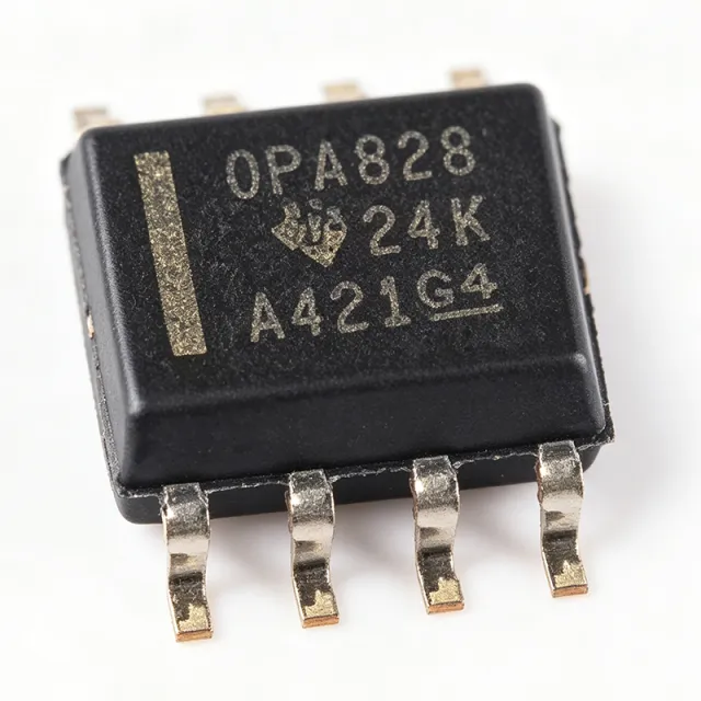
OPA828IDR - 45MHz JFET Op Amp, 4nV/√Hz | TI | Precision Amplifier
The Texas Instruments OPA828IDR is a high-speed, JFET-input operational amplifier delivering 45 MHz gain bandwidth, 150 V/us slew rate, and 4 nV/√Hz voltage noise in an 8-pin SOIC package. It operates over a wide supply range of ±4 V to ±18 V (36 V total) with rail-to-rail output (RRO), positioning it as the next-generation successor to the legendary OPA627 and OPA827 op amps. A JFET-input operational amplifier is a type of precision amplifier whose input stage uses junction field-effect transistors, providing extremely low input bias current (picoampere range) and high input impedance. Within the signal-chain hierarchy, op amps sit between sensors and data converters, serving as the general-purpose analog building block for amplification, filtering, buffering, and transimpedance conversion. Key features include 50 uV input offset voltage, 0.45 uV/C offset drift, 1 pA typical input bias current, and only 60 nVRMS of noise from 0.1 Hz to 10 Hz. These DC precision specifications make the OPA828 suitable for applications where both speed and accuracy are demanded simultaneously - a rare combination. MUX-friendly inputs allow multiplexed signal chains without settling artifacts or charge-injection damage. Architecturally, the OPA828 pairs a JFET input stage with a rail-to-rail output stage, combining classic precision topology with modern output swing. The RRO output maximizes dynamic range in low-voltage systems while the 36 V supply rating supports traditional ±15 V industrial analog rails without redesign. Typical applications include photodiode transimpedance amplifiers (TIA), high-fidelity audio front ends, precision ADC and DAC buffer stages, and active filters in test and measurement instrumentation. The wide 36 V supply range is particularly valuable for industrial designs retaining legacy ±15 V rails. For design, ensure supply decoupling with 0.1 uF ceramic capacitors placed within 3 mm of each supply pin. When replacing an OPA627, verify compensation and bias-current paths, as community feedback shows some legacy TIA circuits require adjustment despite pin compatibility. This page synthesizes distributor pricing, drop-in alternatives, and practical design notes not found in the manufacturer datasheet.

OPA858QIDSGRQ1 - 5.5GHz FET-Input TIA Op-Amp Q1 | TI
The Texas Instruments OPA858QIDSGRQ1 is an automotive-qualified (AEC-Q100), wideband, low-noise decompensated operational amplifier with FET (CMOS) inputs, delivering a 5.5-GHz gain bandwidth product (GBWP) while remaining stable at a minimum gain of 7 V/V. It is supplied in a compact 8-pin WSON (2x2 mm) surface-mount package. A decompensated amplifier is an operational amplifier internally compensated for stable operation only above a minimum closed-loop gain (here 7 V/V). By removing the compensation for unity-gain stability, the decompensated topology achieves dramatically higher bandwidth and lower input-referred noise than unity-gain-stable amplifiers of comparable process technology. In the signal-chain hierarchy, the OPA858-Q1 sits as a wideband voltage-feedback amplifier serving transimpedance amplifier (TIA) and high-gain voltage amplifier roles in high-speed analog front ends. Key features include the 5.5-GHz GBWP that enables high closed-loop bandwidths at transimpedance gains in the range of tens to hundreds of kilo-ohms, FET inputs that minimize input bias current effects on photodiode and high-impedance nodes, and single-ended single-channel configuration optimized for high-speed signal paths. The Q1 variant is manufactured on TI automotive flows and is qualified per AEC-Q100, supporting automotive lidar, imaging, and test applications that demand supply-chain traceability and automotive-grade reliability. The architecture combines CMOS input devices with wideband voltage-feedback internals, yielding low input capacitance that is critical in TIA designs because photodiode plus amplifier input capacitance directly limits achievable bandwidth per unit of transimpedance gain. TI provides the OPA858 together with a companion evaluation module and application collateral covering feedback resistor selection, compensation capacitor sizing, and stability analysis. Typical applications include automotive lidar receiver TIAs, wideband photodiode amplification in optical sensing, high-speed voltage amplification stages, and wideband test and measurement front ends. The device suits any signal chain that requires gain of 7 V/V or higher with multi-hundred-megahertz to gigahertz-class bandwidth. Design consideration: because the amplifier is only stable at gain >= 7 V/V, noise-gain analysis must be performed at all frequencies, including input capacitance effects at the inverting node; verify phase margin with the TI datasheet stability curves before finalizing feedback-network values.

PAM8302A - 2.5W Filterless Class-D Mono Audio Amplifier | Diodes Incorporated
The Diodes Incorporated PAM8302A is a 2.5 W filterless Class-D mono audio amplifier housed in an 8-pin MSOP package, with an additional SOP-8 option. Its CMOS architecture drives 4 ohm or 8 ohm speakers directly without low-pass output filters, saving PCB area and BOM cost while delivering high-quality, low-THD audio reproduction. An audio amplifier is an electronic integrated circuit that boosts a low-power audio input signal to a level capable of driving a loudspeaker or headphones. The Class-D topology uses pulse-width modulation (PWM) to switch the output transistors fully on or fully off, achieving much higher efficiency (typically >85%) than linear Class-AB amplifiers (typically <60%). Within the broader taxonomy, the PAM8302A sits in the audio amplifier IC category, a subset of amplifier ICs, which belong to the signal chain and power management product families. Filterless Class-D amplifiers are particularly valued in portable, battery-powered designs because they eliminate bulky LC output filter networks, reducing both board area and cost. Key specifications include a 2.5 W continuous output power into 4 ohm at 10% THD from a 5.5 V supply, low THD+N of 0.10% at 1 W into 8 ohm, a wide 2.0 V to 5.5 V supply range, integrated undervoltage lockout at 2.1 V, and a low shutdown current. The MSOP-8 (with thermal pad) footprint offers a compact 3.0 mm x 3.0 mm outline suitable for handheld devices, while the SOP-8 (PAM8302AADCR) variant serves designs requiring through-hole-compatible footprints. Built-in short-circuit protection and thermal shutdown further enhance robustness in consumer applications. The PAM8302A employs a fully-differential PWM modulator with proprietary filterless modulation, which eliminates the traditional LC reconstruction filter while maintaining acceptable EMI through controlled edge-rate switching and spread-spectrum techniques. The differential input topology also rejects common-mode noise from upstream audio DACs or PWM sources. Typical applications include portable Bluetooth speakers, handheld gaming consoles, alarm clocks, intercom systems, toys, and any cost-sensitive battery-powered device requiring moderate audio output. Designers frequently choose this part for retrofit audio upgrades in retro gaming hardware, single-board computers, and IoT devices where PCB area is at a premium. When designing with the PAM8302A, ensure adequate power supply bulk decoupling (typically 10 uF) close to the AVDD/PVDD pins to minimize THD. The SD pin (active-low shutdown) must be tied high for normal operation or controlled via a GPIO for power sequencing. Reserve sufficient copper pour on the exposed thermal pad to dissipate Class-D switching losses, especially at full 2.5 W output. This page synthesizes distributor pricing, verified drop-in alternatives, and application-specific design notes not found in the manufacturer datasheet alone, making it a practical engineering reference for sourcing and design.

PAM8403 - 3W Filterless Class-D Stereo Audio Amplifier | Diodes Incorporated
The Diodes Incorporated PAM8403 is a 3 W filterless Class-D stereo audio amplifier delivered in a 16-pin SOP package, operating from a 2.5 V to 5.5 V single supply. Each channel delivers 3 W into a 4 ohm load at 10% THD+N with a 5 V power supply, while maintaining efficiency up to 90% thanks to the Class-D switching topology. The device integrates a bridge-tied load (BTL) output stage that removes the need for external LC low-pass filters on the speaker lines, saving PCB area and BOM cost in stereo and mono consumer audio designs. A Class-D audio amplifier is a switching amplifier topology that uses pulse-width modulation at a switching frequency far above the audio band to recreate the input waveform. Compared with Class-AB linear amplifiers, Class-D parts achieve much higher efficiency (often >85%), which reduces power dissipation in portable and battery-powered applications. The PAM8403 belongs to the audio amplifier IC family, which itself sits inside the broader amplifier IC and integrated circuit hierarchy used in consumer and prosumer audio products. Key features include low THD+N for high-quality sound reproduction, a typical 90% efficiency figure that extends battery life in portable applications, and integrated protection such as short-circuit and thermal shutdown. The shutdown pin (SD) can drive the amplifier into a low-current mute state, and the device also provides a noise-free power-up/power-down cycle that eliminates audible pops. Available only in the SOP-16 package, the part is aimed at compact stereo speaker implementations where board real estate is at a premium. Typical applications include LCD TV and monitor speaker drivers, portable and Bluetooth speaker enclosures, laptop docking stations, DVD and game console line outputs, and phone / speakerphone accessories. Its filterless architecture allows very short, direct PCB traces from the IC outputs to the speakers, simplifying the layout versus traditional Class-D solutions that need an LC reconstruction filter. When designing with the PAM8403, place the supply decoupling capacitors as close to the VDDP and VDDL pins as possible, use a ferrite bead on the speaker outputs if extra EMI suppression is required, and respect the maximum junction temperature rating to avoid thermal shutdown during sustained high-output conditions. This page synthesizes distributor pricing, verified drop-in alternatives, and practical design notes that are not found in the standalone manufacturer datasheet PDF, including PCB layout and EMI considerations specific to filterless Class-D designs.

PGA206UA - 5MHz FET-Input Programmable Gain In-Amp | TI
The Texas Instruments PGA206UA is a high-speed digitally programmable gain instrumentation amplifier (PGA) delivering a 5 MHz bandwidth, 100 pA maximum FET-input bias current, and digitally selectable gains of 1, 2, 4, and 8 V/V in a 16-pin SOIC (SOL-16) surface-mount package. A programmable gain instrumentation amplifier is a precision differential amplifier whose closed-loop gain is set by digital control inputs rather than external resistors. It sits within the amplifier hierarchy as an instrumentation amplifier -> precision op amp -> analog front-end (AFE) -> signal chain IC, combining a true three-architectural-input instrumentation amplifier front end with internally switched gain networks. PGAs are essential in data acquisition systems where a single amplifier must handle sensor signals spanning several orders of magnitude without manual range switching. Key features include fast settling to 0.01% after a gain change, +/-40V input protection that survives overrange faults common in industrial field wiring, and a low maximum offset voltage of 1.5 mV. The FET input stage keeps bias current at 100 pA max, preserving accuracy with high-impedance sources such as pH probes, photodiodes, and piezoelectric sensors. Technically, the PGA206 uses internally switched precision resistor networks controlled by two digital gain-select lines, a scheme the datasheet notes pairs naturally with an external logic latch to acquire gain data from a high-speed digital bus. Slew rate is 25 V/us and the supply range is +/-4.5V to +/-18V, allowing operation from standard +/-5V, +/-12V, or +/-15V analog rails. Operation is specified from -40C to +85C. Typical applications include multi-range data acquisition front ends, programmable sensor interfaces, test and measurement instrumentation, and dynamic signal conditioning where gain must change on-the-fly between measurements. Design consideration: total response time after a gain change equals the switching time plus the settling time to the new output voltage, so budget for settling in high-throughput scanning systems. This page synthesizes distributor pricing, drop-in alternatives, and practical design notes not found in the manufacturer datasheet.
PGA207UA - 5MHz Programmable Gain Instrumentation Amp | TI
The Texas Instruments PGA207UA is a high-speed digitally programmable gain instrumentation amplifier offering a 5 MHz bandwidth, 100 pA maximum FET-input bias current, and digitally selectable gains of 1, 2, 5, and 10 V/V, housed in a 16-pin SOIC (SOL-16) surface-mount package. A programmable gain instrumentation amplifier (PGIA) is a precision differential amplifier whose closed-loop gain is set digitally rather than by external resistors. In the signal-chain hierarchy it sits between sensors and data converters, combining the true instrumentation-amplifier input stage (high common-mode rejection, balanced high-impedance inputs) with gain-switching logic, so a single ADC channel can resolve signals spanning several orders of magnitude. Key features of the PGA207 include two CMOS/TTL-compatible address lines for gain selection, analog inputs internally protected against overloads up to +/-40V even with the supplies off, and laser-trimmed offset voltage for low drift. A fast 0.01% settling specification allows the gain to be switched between conversions in high-throughput data-acquisition systems without dead time. Architecturally, the device uses a three-amplifier instrumentation topology with FET input transistors, giving negligible input bias current (100 pA max) for high-source-impedance sensors, a 25 V/us slew rate, and 18 nV/sqrt(Hz) input noise with 75 dB CMRR. Laser trimming at the Burr-Brown production line holds offset voltage to 1.5 mV max, preserving accuracy at the lowest gains. Typical applications include programmable data-acquisition front ends, dynamic signal ranges from PT100 sensors and strain-gauge bridges, test and measurement instrumentation, and industrial process-control analog front ends feeding 12- to 16-bit ADCs. When designing, remember the gain lines are logic-level inputs: tie them to clean CMOS/TTL levels and route away from the input traces. The +/-40V input protection removes the need for external clamp diodes in most industrial environments. This page consolidates distributor pricing, drop-in family alternatives, and engineering design guidance not found in a single manufacturer datasheet page.
PGA207UA/1K - 5MHz Programmable Gain In-Amp | Texas Instruments
The Texas Instruments PGA207UA/1K is a high-speed, digitally programmable gain instrumentation amplifier delivering gains of 1, 2, 5, and 10 V/V with a 5 MHz bandwidth, a FET input stage with 100 pA maximum bias current, and a 16-pin SOL-16 SOIC surface-mount package. A programmable gain instrumentation amplifier (PGIA) is a precision differential amplifier whose closed-loop gain is set digitally rather than by external resistors. Within the signal-chain hierarchy, it sits between raw transducers and ADCs as a front-end conditioning device, combining the high input impedance and CMRR of a true three-op-amp instrumentation amplifier with gain-switching logic that lets one device serve multiple transducer full-scale ranges. Key features of the PGA207UA/1K include digitally selectable gains (1, 2, 5, 10 V/V) via two CMOS/TTL-compatible address lines, fast settling to 0.01%, a FET input with maximum bias current of 100 pA, and internal input protection rated for plus/minus 40V overloads even with power supplies off. The device is laser-trimmed for low offset voltage (1.5 mV max) and low drift, eliminating manual calibration in most data acquisition designs. Technically, the PGA207 architecture uses a true instrumentation amplifier input stage whose gain is switched by the two digital address lines, so no external gain resistors are needed and gain accuracy is factory-determined. The 5 MHz bandwidth at higher gains supports multiplexed data acquisition channels, while the FET input minimizes loading on high-impedance sources such as photodiodes and piezoelectric sensors. Supply operation spans plus/minus 4.5V to plus/minus 18V, with a slew rate of approximately 25 V/us. Typical applications include multiplexed data acquisition front ends, programmable test and measurement signal conditioning, and industrial sensor interfaces where input channels of different amplitude must share one ADC. Fast settling allows channel-to-channel switching without long dead time, improving system throughput. Design consideration: ensure supply headroom within the plus/minus 4.5V to plus/minus 18V range and route the digital gain-select lines away from the high-impedance inputs to prevent digital noise coupling into the analog front end. This page synthesizes distributor pricing, drop-in family alternatives, comparison data, and practical design notes not found in the manufacturer datasheet.

PGA281 - Zero-Drift Programmable Gain Instrumentation Amplifier | TI
The PGA281 is a high-precision instrumentation amplifier from Texas Instruments featuring digitally-controllable gain and signal-integrity test capability. It uses proprietary autozeroing techniques to achieve low offset voltage, near-zero offset and gain drift, excellent linearity, and nearly no 1/f noise. The device is available in a 16-pin TSSOP package (PW) and operates over a wide supply range, making it suitable for precision sensor interfaces and data acquisition systems. An instrumentation amplifier (INA) is a type of differential amplifier that amplifies the difference between two input signals while rejecting common-mode voltages. It is characterized by high input impedance, high common-mode rejection ratio (CMRR), and low offset voltage. The PGA281 belongs to the family of programmable gain instrumentation amplifiers (PGIAs), which allow the gain to be set digitally or via external resistors, providing flexibility in signal conditioning chains. This category sits within the broader hierarchy of analog amplifiers, which are essential building blocks in electronic systems for signal conditioning and measurement. Key features of the PGA281 include gain programmable from G = 0.2 to 10,000 using an external resistor, fully differential outputs with integrated clamping, low offset voltage of 10 µV (typ) and 35 µV (max), low offset drift of 0.1 µV/°C (typ) and 0.3 µV/°C (max), and low input bias current of 5 pA (typ). These specifications make it ideal for high-accuracy applications where drift and noise are critical. The PGA281 employs a zero-drift architecture that continuously corrects offset and drift, achieving near-zero temperature coefficients. The integrated clamping circuitry protects the outputs from overvoltage conditions, enhancing system robustness. The device supports a wide supply range, typically ±5V, and provides rail-to-rail output swing, maximizing dynamic range. Typical applications include precision current sensing (10 µA to 100 mA), sensor signal conditioning for bridge sensors, thermocouple amplifiers, and data acquisition front-ends. Its low offset and drift make it suitable for medical instrumentation, industrial process control, and test and measurement equipment. When designing with the PGA281, ensure proper decoupling of the power supply pins and consider the thermal performance of the TSSOP package. The gain-setting resistor should be a precision resistor to maintain gain accuracy. The device's signal-integrity test capability allows for system-level diagnostics, which is valuable in safety-critical applications.

SGM8955XN5G - Zero-Drift Op Amp, 1-Ch, SOT-23-5 | SG Micro
The SG Micro SGM8955XN5G is a single-channel, micro-power, CMOS zero-drift operational amplifier housed in a 5-pin SOT-23-5 (XN5) surface-mount package. It delivers a 22 µV (MAX) offset voltage with 80 nV/°C offset drift, 100 dB open-loop gain, and 130 pA input bias current, optimized for precision signal chains operating from low-voltage rails. An operational amplifier (op amp) is a high-gain differential DC amplifier that uses external feedback components to set gain, bandwidth, and transfer characteristics. Zero-drift op amps employ either chopper or auto-zero (chopper-stabilized) architectures to continuously correct offset voltage, eliminating the 1/f flicker noise and offset drift that plague conventional CMOS and bipolar input stages. The SGM8955 belongs to the precision amplifier category within the broader linear IC hierarchy: operational amplifier → amplifier IC → analog signal chain → semiconductor. Key features of the SGM8955XN5G include a 20 µA typical quiescent supply current, 180 V/ms slew rate, rail-to-rail input and rail-to-rail output (RRIO) swing, EMI filtering/RF suppression on the inputs, and an integrated auto-zero calibration loop. The SOT-23-5 (XN5) package operates across -40 °C to +125 °C and supports supply voltages suitable for 2.7 V-5.5 V single-supply systems. The combination of low offset, low drift, low power, and RRIO makes the part a strong fit for battery-powered instrumentation, transducer conditioning, and precision ADC front ends. The SGM8955/6 architecture uses a chopper-stabilized CMOS input stage to achieve sub-50 µV offset, eliminating the periodic recalibration required by conventional CMOS amplifiers in precision applications. The internal EMI/RF input filter rejects high-frequency interference, simplifying PCB layout for sensor applications in electrically noisy environments. The 20 µA quiescent current and low shutdown leakage allow the part to remain continuously powered in battery applications without significantly reducing runtime. Typical applications include high-precision ADC driver circuits, weigh scale and strain gauge signal conditioning, thermocouple and bridge sensor amplifiers, portable medical instrumentation, battery-powered industrial sensors, and zero-drift transducer interfaces. The RRIO capability allows the part to operate at unity gain in single-supply systems where input and output signals swing close to either supply rail. When designing with the SGM8955XN5G, place the input capacitor as close to the op-amp input pins as possible, ensure the feedback network uses 1% or better resistors to maintain gain accuracy, and add an anti-aliasing RC network at the output when driving a downstream ADC. Estimated: total supply current is the sum of the 20 µA quiescent plus the load-dependent output stage current. This page synthesizes distributor pricing, drop-in alternatives, and practical design notes not found in the manufacturer datasheet.
SI8921BD-IS4 - ±250 mV Isolated Amplifier, 5 kV | Skyworks
The Skyworks Solutions SI8921BD-IS4 is a galvanically isolated analog amplifier with a ±250 mV differential input range, 5.0 kV RMS isolation rating, and differential output, housed in a wide-body stretched SOIC-8 package. Key headline specifications include 0.8 µs signal delay, ±0.40 µV typical input offset, ±0.06% typical gain error, 0.5 µV/°C offset drift, and -9 ppm/°C typical gain drift, providing accurate current-shunt measurement across industrial temperature ranges. An isolated amplifier is a type of analog amplifier that combines a precision front-end differential amplifier with a galvanic isolation barrier, transferring the signal across the barrier through capacitive or transformer coupling. The isolation barrier protects low-voltage control circuitry from high-voltage common-mode transients on the field side, enabling safe measurement of floating signals such as those present across current-shunt resistors in motor drives, solar inverters, and uninterruptible power supplies. Within the broader hierarchy, an isolated amplifier belongs to the isolation IC family, which includes digital isolators and isolated gate drivers - all of which form essential building blocks in power-management and industrial-automation systems requiring reinforced insulation per IEC 60747-17 and UL 1577. The SI8921BD-IS4 features a specified input range of ±250 mV, well suited for direct connection across low-ohm shunt resistors in high-current paths. Its differential output swings to a 2.5 V peak full-scale signal, which can be fed directly into the ADC front-end of a motor controller or power-conversion MCU. The device's low offset and drift specifications eliminate the need for periodic calibration in many systems, while its 0.8 µs propagation delay supports closed-loop current control in fast-switching converters. Architecturally, the SI8921BD-IS4 integrates a precision chopper-stabilized input amplifier, a sigma-delta modulator, an isolation capacitor barrier, and a differential output decoder on the low-voltage side. The internal LDO regulators on both sides of the barrier simplify power-supply design - the high-side is powered from a 3.0 V to 5.5 V supply, and the low-side is powered independently from 3.0 V to 5.5 V. The CMOS output stage is capable of driving 2 kΩ loads with low distortion. Typical applications include current-shunt monitoring in three-phase motor drives, photovoltaic inverter string-current sensing, UPS battery-current measurement, industrial process-control isolation, and high-voltage rail monitoring in telecom rectifiers. The differential output interfaces directly with SAR ADCs and sigma-delta converters found in C2000 and PIC32 families. When designing with this device, place bypass capacitors of 0.1 µF and 1 µF close to both VDDA and VDDD pins, keep the input traces short and balanced to preserve CMRR, and observe the creepage and clearance rules of the wide-body SOIC-8 footprint to maintain the 5 kV isolation rating. The differential output should be routed as a matched pair to avoid common-mode pickup in noisy switching environments. This page synthesizes distributor pricing, drop-in alternatives, and practical design notes not found on a single manufacturer product page or distributor listing.
SSM2141PZ - Differential Line Receiver, 100dB CMR, 3MHz | ADI
The Analog Devices SSM2141PZ is an integrated differential line receiver (audio amplifier, Class AB) designed to receive balanced line inputs in professional audio applications requiring high noise immunity and optimum common-mode rejection. Housed in an 8-pin PDIP (PZ) package, it operates from dual supplies of ±6V to ±18V and typically achieves 100 dB of common-mode rejection (CMR) at DC and 60 Hz, far exceeding the ~40 dB CMR achievable with a generic op amp and four discrete precision resistors. The device delivers 0.001% typical THD, a fast 10 V/us slew rate, and a wide 3 MHz small-signal bandwidth. A balanced line receiver is a specialized analog building block that accepts a differential signal riding on a common-mode voltage (such as the long cable run from a stage to a mixing console) and converts it to a single-ended, ground-referenced output while rejecting the common-mode noise picked up along the way. In the audio signal chain hierarchy, the SSM2141 sits between the input connector / XLR stage and downstream ADC or line-level processing; it is part of the broader family of audio amplifiers and instrumentation amplifiers used in pro-audio and broadcast equipment. Key differentiating specifications include 100 dB CMR (DC, typ), 70 dB CMR at 20 kHz and 62 dB at 40 kHz, 0.001% THD+N, 10 V/us slew rate, 3 MHz bandwidth, and a 600 ohm minimum load. Internal thin-film resistor networks are laser-trimmed to deliver matching that no off-the-shelf 0.1% discrete resistor approach can match at production volume, which is what enables the headline CMR figure. Typical applications include balanced audio line receivers in mixing consoles and stage boxes, AES3 / EBU receiver front-ends, audio distribution amplifiers, and instrumentation front-ends where high DC and AC common-mode rejection is required. The 600 ohm load rating and +22 dBu headroom make it directly compatible with broadcast and studio analog line-level standards. When designing with the SSM2141PZ, treat the gain-setting resistor (typically 10 kohm between pins 1 and 8 for unity gain) as a low-noise, low-drift metal-film part to preserve CMR. Add 100 ohm series output resistors plus 10 nF to ground at each output if cable capacitance will exceed ~1000 pF, to prevent oscillation. Decouple both supply pins with 0.1 uF ceramic in parallel with 10 uF tantalum or electrolytic, placed within 5 mm of the package. This page synthesizes distributor pricing, drop-in alternatives, and practical PCB layout notes not found in the manufacturer datasheet alone, including cross-brand substitutes from Texas Instruments and Maxim that share the same 8-pin PDIP footprint and equivalent CMR-class performance.
SSM2142 - Balanced Audio Line Driver, 10 Vrms/600Ω | Analog Devices
The Analog Devices SSM2142 is an integrated differential-output buffer amplifier that converts a single-ended input signal to a balanced (differential) output pair with high output drive capability. Housed in a 16-pin SOIC (or PDIP variant) package, it delivers a transformer-like balanced output capable of driving 10 V RMS into a 600 Ω load, making it a single-chip replacement for discrete audio line-driver circuits that historically required audio output transformers. A balanced line driver, or differential-output audio amplifier, is a specialized analog IC that takes an unbalanced single-ended input and produces two anti-phase outputs whose common-mode noise is rejected by the downstream differential receiver. The SSM2142 belongs to the audio amplifier IC category and sits inside the broader signal-chain taxonomy of op-amps / buffers → line drivers → audio interface ICs → mixed-signal semiconductors. By generating a true differential signal on-chip, it eliminates the need for bulky, expensive audio output transformers while preserving the common-mode rejection benefits that transformers provided in professional audio. Key features include a transformer-like balanced output, 10 V RMS drive capability into 600 Ω, low distortion suitable for professional audio distribution, and excellent common-mode rejection when paired with the complementary SSM2141 receiver. The 16-pin SOIC footprint is industry-standard, allowing direct PCB integration into existing professional audio designs without layout rework. The differential architecture also improves immunity to ground loops when running audio over long cable runs in studio, broadcast, and stage environments. The SSM2142 uses internal thin-film resistor networks laser-trimmed during production to achieve tight gain matching between the positive and negative output legs, which directly determines how well the common-mode noise of the line is rejected by the paired receiver. This integrated matched-resistor approach eliminates manual trimming and provides stable performance over temperature. The amplifier can drive the full pro-audio level of +24 dBu (12.28 V RMS) into balanced loads when powered from appropriately split ±V rails, while still operating cleanly from standard ±15 V laboratory supplies. Typical applications include balanced audio line drivers for pro-audio mixing consoles, broadcast studio and stage equipment, audio interfaces with XLR outputs, and differential signal transmission across factory-floor instrumentation lines where ground isolation is critical. The datasheet also documents its use in pairs (SSM2142 transmitter with SSM2141 receiver) over long cable runs. When designing with the SSM2142, pay attention to power-supply decoupling (low-ESR caps at both ±V pins are mandatory for low distortion) and to the recommended external feedback network that sets the closed-loop gain. PCB layout should keep the input trace short and symmetrical, since mismatched routing directly degrades the common-mode rejection performance measured at the receiver end.