دوائر المضخم المتكاملة
المنتجات (1,100+)
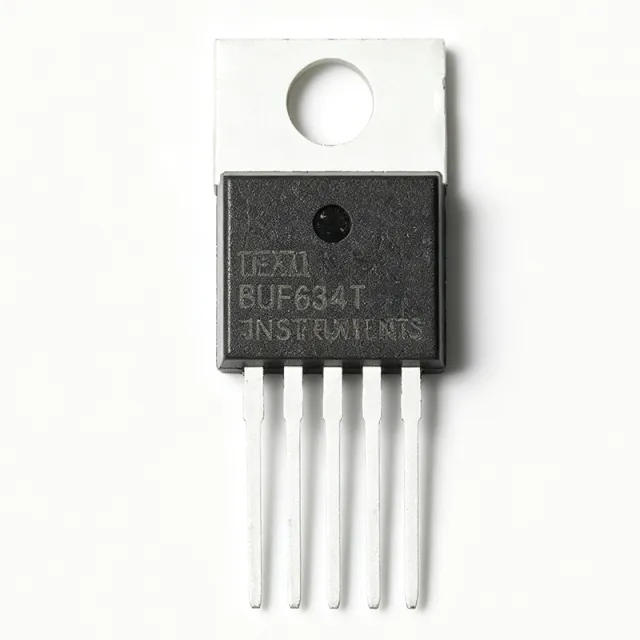
BUF634T - 250mA High-Speed Buffer, 2000V/us | Texas Instruments
The Texas Instruments BUF634T is a 250 mA high-speed, unity-gain, open-loop buffer amplifier with a 2000 V/us slew rate, pin-selected 180 MHz bandwidth, and a wide supply range of up to plus or minus 18 V, housed in a 5-pin TO-220-5 package. A buffer amplifier (also called a unity-gain voltage follower) is a specialized amplifier stage with a gain of one that isolates a high-impedance source from a low-impedance load. In the signal-chain hierarchy, buffers sit between operational amplifiers and their loads: an op amp provides voltage gain while the buffer provides current gain, preventing load-induced distortion and thermal feedback inside the gain element. Buffers are a core building block of analog power management and output driver design. Key features of the BUF634T include 250 mA of continuous output current, an extremely fast 2000 V/us slew rate, and a unique pin-selected bandwidth mode: connecting the BW pin to V- enables the full 180 MHz bandwidth (1.5 mA typical quiescent... 30 MHz mode draws only 1.5 mA... full 180 MHz mode draws approximately 11 mA). Internal current limiting and thermal shutdown protection provide robustness against output shorts and overloads. The device is fabricated on a bipolar process optimized for speed and drive capability rather than precision offset. Architecturally, the BUF634 is a completely open-loop, unity-gain buffer, so it adds no phase shift from feedback compensation and can be placed inside an op amp feedback loop to boost output current, eliminate thermal feedback errors in the op amp input stage, and improve capacitive load drive without oscillation risk. Typical applications include headphone amplifier output stages (a classic pairing with the OPA627 or OPA134), video distribution and line driving, op amp output current boosting for test and measurement instrumentation, and capacitive load isolation for ADC input drivers and cable drivers. Design consideration: the BUF634T is not a precision amplifier - offset voltage and drift are far looser than a precision op amp, so place it inside an overall feedback loop when DC accuracy matters. Power dissipation scales with load current and supply headroom, so the TO-220-5 tab should be heat-sunk for sustained high-current operation. This page synthesizes distributor pricing, drop-in alternative analysis, and practical design notes not found in the manufacturer datasheet.

BUF634U - 250mA, 180MHz High-Speed Buffer | Texas Instruments
The Texas Instruments BUF634U is a 250 mA high-speed unity-gain open-loop buffer amplifier featuring a 2000 V/us slew rate and a pin-selected bandwidth of up to 180 MHz, housed in an 8-pin SOIC (SO-8, 3.90 mm width) surface-mount package. A buffer amplifier is a unity-gain voltage follower that isolates a high-impedance source from a low-impedance load while delivering substantial output current. Within the power-management and signal-chain hierarchy, buffers sit between amplifiers and loads, extending the drive capability of operational amplifiers, ADCs, and filters. Buffers trade voltage gain for current gain, and the BUF634 is a classic open-loop buffer architecture in which the output stage is driven directly by the input, minimizing transient distortion. Key features include 250 mA of output current, a 2000 V/us slew rate that preserves fast edges, a wide supply range of +/-2.25 V to +/-18 V (4.5 V to 36 V total), and a low 1.5 mA quiescent current when operated in the 30 MHz low-power bandwidth mode selected via the bandwidth pin. Internal current limiting and thermal shutdown protection guard the device against overload faults. Technically, the BUF634 combines a high-speed bipolar input stage with a push-pull class-AB output stage. The pin-selected bandwidth (30 MHz or 180 MHz) lets designers trade quiescent power for speed: low-power mode suits battery and portable designs, while full-bandwidth mode supports fast pulse and video signal chains. Because it is open-loop, phase reversal is not an issue and it can be placed inside an op-amp feedback loop to boost output current, eliminate thermal feedback on the input stage, and improve capacitive load drive. Typical applications include op-amp output current boosting in instrumentation amplifiers, line drivers for video and communications, headroom-limited audio headphone amplifiers, and capacitive-load driving in data-acquisition front ends. A key design consideration: the bandwidth-select pin must be tied appropriately (to V- for 180 MHz or open with capacitor for 30 MHz); leaving it floating can produce unpredictable frequency response. Note that the BUF634U is designated not recommended for new designs (NRND); TI recommends the BUF634A as a pin-compatible upgrade. This page synthesizes distributor pricing, drop-in alternatives, application guidance, and lifecycle information not consolidated in the manufacturer datasheet.
BUF634U-VB - 250mA High-Speed Buffer, 180MHz SOIC-8 | Texas Instruments
The Texas Instruments BUF634U-VB (BUF634U) is a 250 mA high-speed, unity-gain, open-loop buffer with a 2000 V/us slew rate, pin-selected bandwidth up to 180 MHz, and a wide supply range of +/-2.25 V to +/-18 V, housed in an 8-pin SOIC package. A buffer amplifier is a unity-gain stage whose purpose is to isolate a high-impedance source from a low-impedance load while passing the signal without amplification. In the signal-chain hierarchy, the buffer sits between a precision op amp and its load, providing current gain and drive capability that the op amp alone cannot deliver. High-speed buffers like the BUF634 family are essential building blocks in analog front-end design. Key features include a continuous output current of 250 mA, a 2000 V/us slew rate for fast large-signal edges, and a bandwidth that is pin-selectable between 30 MHz, 130 MHz, and 180 MHz, allowing designers to trade bandwidth against quiescent current - only 1.5 mA at the 30 MHz setting. Internal current limiting and thermal shutdown protection guard against fault conditions. Architecturally, the BUF634 is an open-loop bipolar buffer with no internal feedback compensation, which means it adds essentially no phase shift when placed inside an op amp feedback loop. This lets it boost op amp output current, eliminate thermal-feedback-induced errors, and improve capacitive-load drive without degrading loop stability. Typical applications include buffering the output of precision op amps such as the OPA-series in test and measurement instrumentation, driving ADC input or reference networks, and serving as a current booster inside audio or video line-driver loops. Design consideration: the bandwidth pin (BW) sets quiescent current, so choose the lowest bandwidth setting that meets signal requirements to minimize power dissipation and thermal rise in the SOIC-8 package. This page synthesizes verified distributor pricing, drop-in alternative analysis, and practical design guidance not found in the manufacturer datasheet.
BUF634U/2K5 - 250mA 180MHz High-Speed Buffer | TI
The Texas Instruments BUF634U/2K5 is a 250mA high-speed unity-gain open-loop buffer amplifier with 180MHz bandwidth, 2000 V/µs slew rate, and a wide ±18V (36V single-supply) operating range, housed in an 8-pin SOIC (D) package supplied in tape and reel. A high-speed buffer is a unity-gain amplifier optimized for output current drive and bandwidth rather than voltage gain. In the power-management and signal-chain hierarchy, it sits between an op amp and a load, extending the load-driving capability of precision amplifiers. Buffers like the BUF634 belong to the buffer amplifier family of analog ICs and are commonly placed inside an op amp feedback loop to raise output current, isolate capacitive loads, and eliminate thermal-feedback-induced distortion. Key features of the BUF634U/2K5 include 250mA output current with internal current limiting, pin-selectable bandwidth of 180MHz (full bandwidth) or 30MHz with only 1.5mA quiescent current, and thermal shutdown protection. This bandwidth-selection pin lets designers trade speed for power, making the device equally at home in fast pulse applications and battery-conscious designs. The 2000 V/µs slew rate supports large-signal high-frequency signals without slew limiting. The BUF634 uses an open-loop, high-current class-AB output topology with a quiescent bias that scales with the selected bandwidth setting. Because it operates open-loop, its gain is fixed near unity with high input impedance (5µA input bias current) and a 30mV input offset voltage, so it is normally embedded within an op amp feedback loop where loop gain corrects its offsets and gain error. Typical applications include op amp output boost stages in line drivers and ATE, laser-diode and piezo drivers, video distribution, cable and test instrumentation drivers, and capacitive-load isolation for precision amplifiers such as the OPA series. A key design consideration is thermal management: driving 250mA continuously at high supply voltage can exceed package dissipation, so copper area on the SOIC-8 footprint and the thermal shutdown threshold must be accounted for in the design. This page synthesizes distributor pricing, drop-in alternatives, pinout data, and practical design notes beyond what the manufacturer datasheet alone provides. Pricing references are as of 2026-09-13.

CA3420AE - BiMOS Op-Amp, 0.5MHz, Low-V, pA Input | Renesas
The Renesas CA3420AE is a 0.5 MHz low-supply-voltage operational amplifier that integrates PMOS and bipolar devices (BiMOS) on a single monolithic die, housed in an 8-pin PDIP package. The CA3420A grade (suffix 'A') provides tighter input offset voltage specifications than the standard CA3420, with typical input bias currents below 1 pA and operation from a single supply as low as 2 V (and up to 15 V). According to the Renesas/Intersil datasheet, the CA3420AE uses gate-protected PMOS transistors in the input stage to deliver extremely high input impedance, making it well suited for transducer buffers, electrometer-style front ends, and any application where leakage from the op-amp input would otherwise corrupt a high-impedance signal. What is a BiMOS operational amplifier? A BiMOS op-amp is a hybrid analog integrated circuit that combines the high input impedance and ultra-low input current of PMOS transistors with the strong drive capability and DC precision of bipolar transistors. This places the BiMOS family in the broader taxonomy: operational amplifier -> amplifier IC -> linear IC -> analog signal chain -> semiconductor. Compared with a pure bipolar op-amp, a BiMOS part offers several picoamperes of input bias (rather than nanoamperes), and compared with a CMOS op-amp, a BiMOS part typically delivers higher output drive and better DC accuracy. Key features include 0.5 MHz unity-gain bandwidth, internal phase compensation for unity-gain stability, a unique bootstrapped guardbanding network that minimizes leakage, and rail-to-rail-ground sensing on the low side. The PMOS input pair gives the CA3420AE an input impedance exceeding 1 Tohm, and the bipolar output stage can swing within millivolts of ground while sinking several milliamps - a useful trait when the supply is only a few volts and headroom is at a premium. The CA3420AE is internally compensated and designed to operate from a single 2 V to 15 V supply (or dual ±1 V to ±7.5 V), making it compatible with low-voltage battery and legacy ±5 V analog rails. The bipolar output stage, combined with the PMOS input pair, gives the part its distinctive low-input-current / moderate-drive profile. Typical applications include pH and ion-selective electrode buffers, photodiode transimpedance preamps, precision long-time-constant integrators, sample-and-hold circuits, and high-impedance sensor signal conditioning. The wide supply range and single-supply ground-sensing capability make it a strong fit for battery-powered instrumentation as well as industrial process-control front ends. When designing with the CA3420AE, observe that the bipolar output stage cannot swing fully to the positive rail - typically leaving roughly 1 V of headroom - so design the surrounding circuit with appropriate margin. Input traces should be guarded to fully realize the 1 pA input bias advantage; unterminated high-impedance nodes will pick up 50/60 Hz hum and any nearby leakage. This page synthesizes Renesas datasheet specifications, distributor pricing snapshots, and pin-compatible cross references for engineers evaluating the CA3420AE for low-leakage precision analog front ends.
CA3420E - 0.5MHz BiMOS Op-Amp 8-PDIP | Renesas
The Renesas CA3420E is a 0.5 MHz, low-supply-voltage, low-input-current BiMOS operational amplifier housed in an 8-pin PDIP through-hole package. It combines PMOS input transistors with bipolar output devices on a single monolithic die, delivering rail-to-rail output swing, sub-picoampere input bias current, and operation from a 2 V to 15 V single rail (or ±1 V to ±7.5 V dual). The CA3420E is a general-purpose single-channel op-amp designed for high-impedance front-ends where CMOS-class I_B cannot be matched by classic bipolar parts. A BiMOS operational amplifier is a hybrid analog IC architecture that marries the high input impedance and near-zero gate current of PMOS transistors at the input stage with the high transconductance, high slew capability, and low offset drift of bipolar transistors at the gain and output stages. Within the broader taxonomy, BiMOS op-amps sit between pure CMOS op-amps (lowest I_B, lowest noise, lowest speed) and pure bipolar op-amps (highest speed, higher I_B). They occupy the use-case niche of picoampere-input instrumentation, charge amplifiers, pH/ORP electrodes, photodiode transimpedance, and high-impedance buffers where neither extreme of the trade-off curve is acceptable. Key features of the CA3420E include an input bias current below 1 pA (typical), rail-to-rail output swing, a unity-gain bandwidth of approximately 0.5 MHz, single-supply operation as low as 2 V, and internal gate-protection diodes on the PMOS inputs. The internal bootstrap network provides a unique guardbanding scheme that reduces leakage paths, an important advantage in high-temperature or high-humidity environments where PCB contamination would otherwise dominate leakage. The DIP-8 package simplifies breadboarding, socket replacement of legacy designs, and through-hole repair workflows in industrial instrumentation. Architecturally, the input differential pair uses PMOS transistors with on-chip gate protection. The second stage is bipolar, and the output is a bipolar class-B push-pull capable of rail-to-rail swing. The combination produces low input current, modest GBW, low quiescent current, and adequate phase margin for unity-gain buffer operation. The CA3420 is the broader family; the CA3420E denotes the 8-PDIP package, with the CA3420EZ being the SOIC-8 variant. An automotive/extended-screening grade CA3420E/AE also exists. Typical applications include pH and ORP probe buffers, photodiode transimpedance front-ends, electrometer-grade instrumentation, ion-selective electrode amplifiers, smoke-detector ionization-chamber interfaces, and legacy analog signal chains designed around CA3420 generations. The combination of sub-picoampere I_B and rail-to-rail output is rare and useful in battery-powered portable instrumentation. When designing with this device, note that the 0.5 MHz GBW restricts use to DC and low-frequency signal chains. For higher-speed applications (>100 kHz full-power), a different op-amp topology is required. Input protection against ESD strikes beyond the internal diodes is recommended for handheld probes.

CS5203A-HGZ - High-Temp Ceramic Geophone Amp | Cirrus Logic
The Cirrus Logic CS5203A-HGZ is a high-temperature ceramic-geophone amplifier integrated circuit, factory-qualified for operation in extended-temperature downhole and seismic acquisition environments. Housed in a hermetic ceramic package optimized for thermal stress tolerance, the CS5203A-HGZ delivers a low-noise differential amplification path tuned for the microvolt-level signals produced by geophone sensors deployed in oilfield exploration, geothermal monitoring, and vibration analysis systems. Geophone amplifiers form the front-end signal chain in seismic acquisition systems; they convert the small differential voltages generated by moving-coil geophone sensors into usable analog signals while rejecting common-mode noise picked up from long cable runs in the field. The CS5203A-HGZ is engineered specifically for high-temperature ceramic-geophone use, where standard plastic-encapsulated amplifiers would suffer from thermal drift, package cracking, or accelerated aging. The '-HGZ' suffix denotes the high-temp ceramic package grade, distinguishing it from commercial-grade equivalents. Key features include an extended operating temperature range suitable for downhole environments, low input-referred noise for faithful recovery of weak seismic reflections, and a differential input topology that suppresses common-mode cable noise. The ceramic package provides robust mechanical stability across thermal cycling. The amplifier operates from a low quiescent current, preserving battery life in remote, unattended seismic recorder nodes. Typical applications include seismic acquisition systems, oil and gas downhole geophone sensing, geothermal and volcano monitoring instrumentation, surface vibration analysis for civil engineering, and any harsh-environment MEMS or geophone signal-conditioning front end. The part is also used in academic seismology field stations requiring long-term unattended deployment. When designing with the CS5203A-HGZ, verify that downstream ADC input range matches the amplifier's differential output swing and provide proper input common-mode biasing. Place bypass capacitors close to the supply pins and keep the geophone cable shield bonded to a clean analog ground to maximize common-mode rejection in field installations.

E-TDA7391PDTR - 2x40W Dual BTL Audio Amplifier | STMicroelectronics
The E-TDA7391PDTR is a dual-channel bridge-tied load (BTL) audio power amplifier from STMicroelectronics, designed for high-quality car radio and multimedia applications. It delivers up to 2x40W of output power into a 4-ohm load with a 14.4V supply, making it a robust solution for automotive audio systems. The device is housed in a PowerSO-20 package, which provides excellent thermal performance for high-power operation. An audio power amplifier is an electronic device that increases the amplitude of audio frequency signals to drive loudspeakers. In the hierarchy of audio electronics, a BTL amplifier is a type of linear amplifier that uses a bridge configuration to double the voltage swing across the load, effectively quadrupling the output power compared to a single-ended amplifier with the same supply voltage. This makes BTL amplifiers ideal for automotive applications where the battery voltage is limited to 12V or 14.4V, and high output power is required without using bulky transformers or switching converters. Key features of the E-TDA7391PDTR include a wide operating supply voltage range of 8V to 18V, a low quiescent current of 120mA, and a high output power of 40W per channel at 10% THD. The device also features standby and mute functions for power management, a pop-free turn-on/off sequence, and full short-circuit and thermal protection. The PowerSO-20 package has an exposed pad that enhances heat dissipation, allowing continuous operation at high power levels without external heatsinks in many applications. The E-TDA7391PDTR uses a complementary NPN/PNP output stage with a class-AB biasing scheme, which provides low crossover distortion and high linearity. The device incorporates a sophisticated protection circuitry that includes output short-circuit protection, over-temperature shutdown, and load dump protection, ensuring reliable operation in harsh automotive environments. The standby and mute pins allow for easy system-level power management, reducing power consumption when the audio system is not in use. Typical applications include car radio head units, multimedia systems, and aftermarket audio amplifiers. The high output power and low distortion make it suitable for driving mid-range and subwoofer speakers in automotive sound systems. The device can also be used in home theater systems and portable PA systems where a compact, high-power amplifier is required. When designing with the E-TDA7391PDTR, it is essential to provide adequate power supply decoupling with a 1000uF electrolytic capacitor and a 100nF ceramic capacitor close to the supply pins. The exposed pad must be soldered to a large copper area on the PCB to ensure proper thermal management. Additionally, the standby and mute pins should be controlled with a microcontroller or a simple RC network to ensure a pop-free power-up sequence.

EL4340 - 500MHz Triple 2:1 Mux Video Amplifier | Renesas
The Renesas EL4340 is a 500 MHz triple, fixed-unity-gain, 2:1 multiplexing amplifier (mux amp) engineered for high-speed video switching and RGB routing applications. Housed in a 24-pin QSOP (24-QSOP, IUZ suffix) package, the device integrates three independent 2:1 input multiplexers feeding three fixed-gain of 1 output buffers, supporting RGB/YPbPr/1080p/UXGA video formats with minimal channel-to-channel skew. Key features include 500 MHz small-signal bandwidth at -3 dB, an 800 V/us slew rate (typical), a high-impedance output disable (HIZ) state that allows multiple device outputs to be wire-OR'd onto a shared output bus, and a per-channel ENABLE (power-down) pin that drops quiescent current in unselected channels for power-sensitive portable video designs. Output drive supports 2 Vp-p into 150 ohm back-terminated video loads. Internally the EL4340 uses a current-feedback architecture with three matched transimpedance input stages and high-speed complementary output stages. The unity-gain buffer simplifies board layout by eliminating feedback components, while the integrated 2:1 input mux eliminates the need for external mechanical or relay switching. Each channel has independent logic inputs (INA0/INA1, INB0/INB1, INC0/INC1) plus HIZ and EN control lines, allowing flexible source selection for triple-channel video systems. Typical applications include RGB video routers, video-on-demand switches, A/V receivers, projectors, broadcast studio equipment, surveillance systems, and digital signage. The HIZ and EN features make it especially attractive for large matrix switches where outputs of multiple EL4340 devices are bussed together. The wide supply range (single 5V or +/-5V) supports both portable and AC-powered systems. When designing with the EL4340, keep the analog input traces matched in length and impedance (75 ohm typical for video) and place 0.1 uF decoupling capacitors within 5 mm of each supply pin. Use 75 ohm back-termination at the output when driving long cable runs to absorb reflections. Drive ENABLE high only when the channel is active to minimize total system power.

EL4543 - Triple Differential Twisted-Pair Driver | Renesas
The Renesas EL4543 is a high-bandwidth triple differential amplifier with integrated encoding of video sync signals, housed in either a 24-pin QSOP or 20-pin QFN package. It delivers three matched differential line drivers optimized for twisted-pair video transport (UTP/STP), with bandwidth sufficient for SDTV, EDTV, and HDTV video formats. The common-mode input range extends all the way to the negative rail, enabling ground-referenced signalling in single-supply applications from +5 V or +3.3 V rails without level shifting. A differential line driver is an amplifier that converts a single-ended input into two complementary outputs whose voltage difference carries the signal; this architecture rejects common-mode noise picked up along a transmission cable, which is critical for long twisted-pair runs in security and pro-AV installations. As a member of the video amplifier family (differential amplifier -> video amplifier -> analog interface IC -> signal chain IC), the EL4543 integrates sync encoding that overlays horizontal and vertical sync information onto the common-mode voltage of the differential pair, allowing the receiver to recover timing from any conductor of the pair. Key features include three fully differential output channels, an integrated sync encoder that maps composite sync onto the common-mode level, support for single-ended or differential input signals, and ground-referenced input common-mode range to the negative rail. The high bandwidth enables clean reproduction of component video (YPbPr) and RGB signals over Cat5/Cat6 cabling with minimal crosstalk between the three pairs. Typical applications include CCTV camera-to-DVR transmission over UTP, KVM extenders, RGB video over Cat5 distribution systems, and studio video routing over twisted-pair infrastructure. Compared with discrete line-driver implementations, the EL4543 replaces multiple op-amps, sync insertion circuits, and bias networks, reducing PCB area and BOM cost while improving channel-to-channel matching. When designing with the EL4543, choose between the QSOP (EL4543IUZ) and QFN (EL4543ILZ) package based on assembly preference; both share electrical characteristics. Maintain a clean +5 V analog supply with adequate decoupling (1 µF + 0.1 µF) at each supply pin, and provide 75 Ω cable-side termination at each differential output to match characteristic impedance. This page synthesizes distributor stock, parametric comparisons with alternative triple differential drivers, and practical PCB layout guidance not collated in the manufacturer datasheet.

EL4543IUZ - Triple Differential Twisted-Pair Video Driver | Renesas
The Renesas EL4543IUZ is a high-bandwidth triple differential amplifier with integrated common-mode sync encoding, designed as a twisted-pair video line driver, supplied in a 24-lead QSOP package rated from -40C to +85C. A differential line driver is an amplifier stage that converts a single-ended or differential input signal into a balanced differential output pair suitable for transmission over twisted-pair or coaxial cable. Within the signal-chain hierarchy, it sits between a video source (encoder, GPU, camera sensor output) and the cable plant, complementing a differential receiver at the far end. Balanced transmission rejects common-mode noise picked up on the cable, which is why differential line drivers are the standard solution for long video links in KVM extenders, industrial displays, and automotive video systems. Key features of the EL4543 include three fully differential high-speed amplifier channels capable of handling high-resolution composite video, integrated encoding of video sync signals onto the common-mode of the output pairs (eliminating a separate sync channel and reducing cable count), and an input common-mode range that extends all the way to the negative rail. That rail-to-negative common-mode capability permits simple ground-referenced input termination in single-supply systems, removing the need for input level-shifting circuitry. The part accepts inputs in either single-ended or differential form, giving designers flexibility at the source interface. Technically, each channel drives a twisted pair with a balanced output whose sync information rides on the common-mode voltage, so a standard differential receiver with common-mode detection can recover both video and timing. Integrating three channels plus sync encoding in one IC delivers significant system cost savings versus discrete line-driver alternatives, per the manufacturer datasheet, cutting BOM count, board area, and channel-to-channel skew. Typical applications include KVM and video extender transmitter boards, driving high-resolution video over Cat5-class twisted pair, security camera video distribution, and industrial display links where sync and video must share one cable run. A key design consideration is supply decoupling and output termination: differential drivers require tight layout around each output pair and correct cable-side termination to preserve return-loss and minimize radiated emissions at video frequencies. This page adds value beyond the datasheet by compiling drop-in part variants, pricing tiers, design notes, and application guidance sourced from Renesas and distributor data.

EL5160 - 200MHz Low-Power Current Feedback Amplifier | Renesas
The Renesas EL5160 (originally Intersil) is a single low-power current-feedback operational amplifier delivering a wide -3dB bandwidth of 200MHz while drawing only 0.75mA of supply current per amplifier, housed in a 6-lead SOT-23 or 8-lead SOIC package operating over the industrial -40C to +85C temperature range. A current-feedback amplifier (CFA) is a type of operational amplifier whose architecture senses error current rather than error voltage at its input stage. In the power-management and signal-chain hierarchy, the CFA sits under the amplifier family alongside voltage-feedback op amps, but its closed-loop bandwidth is largely set by the feedback resistor rather than the gain-bandwidth product, allowing the EL5160 to maintain near-constant 200MHz bandwidth across useful gain settings. Key differentiating specifications include the 200MHz -3dB bandwidth, an extremely low 0.75mA supply current per amplifier, and an enable function (EL5160 variant) that permits power savings in multiplexed or strobed video signal paths. The output stage is capable of driving 50-ohm loads toward both supply rails, which is unusual for a micropower amplifier and simplifies direct drive of video cables and monitor inputs. Architecturally, the current-feedback topology yields high slew rate and fast settling without the classic gain-bandwidth trade-off of voltage-feedback designs. The family also includes the EL5161 (single, no enable), EL5260/EL5261 (dual) and EL5360 (quad), letting designers scale channel count while reusing the same 200MHz/0.75mA performance envelope. Typical applications include high-speed video signal distribution, CRT/LCD monitor front ends, video switching and buffering, and portable or battery-powered instrumentation where the 0.75mA quiescent draw extends battery life. Design considerations: because bandwidth depends on the feedback resistor, use the datasheet-recommended RF value; deviations directly shift the -3dB corner and peaking behavior. This page synthesizes verified manufacturer datasheet content, family cross-references, applications guidance and pricing context not consolidated in the Renesas datasheet alone.
EL5306 - Triple 350MHz Fixed Gain Amplifier | Renesas
The Renesas EL5306 (originally Intersil) is a triple 350MHz fixed gain amplifier with enable function, operating from a single 5V to 12V supply (or dual supplies from ±2.5V to ±5V) at just 1.5mA per amplifier supply current, housed in a 16-lead SOIC or QSOP package. A fixed gain amplifier is a type of high-speed voltage feedback amplifier in which the gain-setting network is internal, eliminating external gain resistors and the layout parasitics and tolerance errors they introduce. Within the signal-chain hierarchy, it sits between general-purpose op amps and dedicated video buffers, and belongs to the broader family of high-speed amplifiers and analog signal conditioning ICs. Key features include a 350MHz bandwidth tuned for high-speed video and monitor applications, internal gain-setting resistors configurable in gains of +1, -1 or +2, a power-saving enable/disable function that reduces supply current to 25uA typical per amplifier, and very low differential gain and phase of 0.02% and 0.04 degrees while driving 150 ohm loads at a gain of 2. Technically, the EL5306 uses special internal circuitry that reduces the variation of output impedance with output current, which directly delivers the excellent dG/dP video performance. Its low 1.5mA per-amplifier supply current combined with 350MHz bandwidth makes it well suited to portable, handheld, and battery-powered equipment, per the manufacturer datasheet. The device operates over the industrial temperature range to +85C. Typical applications include high-resolution video signal distribution in monitors, video line driving, and multi-channel high-bandwidth signal conditioning in portable test and communication equipment. A key design consideration: the amplifier is specified for supply spans of at least 5V and up to 11V; operate it within 5V to 10V single-supply or ±2.5V to ±5V dual-supply to maintain rated bandwidth and video performance. This page synthesizes verified datasheet parameters, application guidance, and drop-in alternative analysis not found on standard distributor product pages.
GX36220 - 2x64Gb/s Dual Linear TIA for 400G Coherent ROSA | Renesas
The Renesas GX36220 is a dual-channel linear Trans-Impedance Amplifier (TIA) designed for 400G coherent Receiver Optical Sub-Assemblies (ROSAs), delivering 2x64Gb/s aggregate bandwidth across two integrated TIA signal paths for I and Q channels. Housed as a bare die (DIE SALE), each channel supports 32Gb/s symbol rate operation to enable DP-16QAM and higher-order modulation formats used in next-generation coherent optical transceivers. An LDO (Low-Dropout) linear regulator is a class of voltage regulator that maintains a stable output voltage even when the supply rail is only marginally above the desired output. In this product family of high-speed analog amplifiers, linearity and low input-referred noise are paramount: the TIA converts small photodiode currents into usable voltage swings while preserving the modulation fidelity required for soft-decision FEC at 400G and beyond. The GX36220 sits within the linear amplifier hierarchy, which bridges photodetectors and the host CDR/DSP in the optical receive chain. Key differentiating specifications include a per-channel bandwidth of approximately 28 GHz to support 32Gbaud Nyquist operation, very low input-referred noise current on the order of sub-pA/sqrt(Hz), and a differential trans-impedance in the multi-kΩ range typical for coherent I-channel amplifiers. The device integrates two matched TIA cores on a single die, removing the need for a second IC in dual-polarization receivers. The die form factor is required for sub-pF parasitic bonding directly to the photodiodes and to the limiting-stage or CDR ASIC, minimizing stub lengths. Architecture-wise, the GX36220 is built on a high-fT SiGe BiCMOS process that delivers the fT/ft necessary for 32Gbaud I/Q paths. Auto-zero feedback and on-die bias networks hold the operating points stable across temperature. The dual-channel layout is symmetrical so that I and Q skew is minimized, which is critical for coherent demodulation where timing mismatch translates directly into phase-error penalties. Typical applications include 400G CFP2-DCO and QSFP-DD coherent transceivers, line-card ROSAs for DWDM transport platforms, and OEM 600G/800G next-generation coherent reference designs. The bare-die format means the part is wire-bonded inside a hermetic ROSA package alongside InP photodiodes or integrated coherent receivers. When designing with this device, follow Renesas evaluation board layout guidelines to keep bond-wire inductance below 0.5 nH per tap. Use matched differential routing on host side and provide a quiet low-noise analog supply. Thermal management is handled at the ROSA package level since the GX36220 ships as a bare die. This page synthesizes distributor pricing snapshots, cross-reference data, and engineering design notes that go beyond the manufacturer datasheet to assist BOM and qualification engineers.
GX36220-F-DNT - 2x64Gbps Linear TIA | Renesas Electronics
The Renesas Electronics GX36220-F-DNT is a dual-channel (2x) 64 Gbps linear transimpedance amplifier (TIA) supplied in bare-die form (DNT package code) for fiber-optic communication systems. It belongs to Renesas' telecom IC amplifier portfolio targeting next-generation optical interconnects. A transimpedance amplifier (TIA) is an analog amplifier that converts a current input, typically from a photodiode, into a voltage output with gain expressed in ohms (V/A). In the optical-module hierarchy, the TIA sits directly behind the photodetector (PD) in the receive path, feeding a limiting amplifier or linear equalizer, then a clock-and-data-recovery (CDR) unit - forming the optical receiver signal chain of a power management and signal-conditioning sub-system. Linear TIAs such as this device preserve waveform amplitude information, which is required for PAM4 reception and DSP-based equalization in high-speed links. The GX36220 integrates two independent TIA channels on one die, enabling compact dual-lane optical subassemblies such as OSFP, QSFP-DD, and CDFP-based 100-400 Gbps module implementations. The linear output architecture supports both NRZ and multi-level PAM4 signaling, allowing the downstream DSP or CDR to perform the slicing decision. Being supplied as a bare die (Telecom IC Amplifier Die per DigiKey classification), the device is intended for direct die-attach into optoelectronic packages, typically co-packaged with photodiodes in TO-can or butterfly subassemblies by module manufacturers. It is not a board-level packaged component; die-level handling, bond-pad design, and assembly require appropriate cleanroom and wire-bond capability. Typical applications include 400G/800G data-center optical transceiver receive paths, telecom coherent receiver front ends, active optical cables, and test instrumentation optical front ends where dual-channel density and 64 Gbps-per-lane linearity are required. Design consideration: because this is a die product, electrical performance is strongly dependent on bond-wire inductance, photodiode capacitance, and bias network layout; consult the Renesas datasheet for reference bond-out configurations before finalizing the subassembly. This page synthesizes distributor pricing, lifecycle, and sourcing data for the GX36220-F-DNT that is otherwise fragmented across multiple distributor listings.
GX36420 - 64 Gbps Quad Linear TIA for 400G/600G Coherent | Renesas
The Renesas GX36420 is a 64 Gbps linear quad transimpedance amplifier (TIA) chip integrating four independent TIA lanes (XI, XQ, YI, YQ) plus on-die DC-control digital interface circuitry on a single die. It is targeted at 400G and 600G coherent optical receivers in DWDM line-card applications. The bare-die form factor is supplied as tested wafer (DNT) for hybrid integration with photodiode arrays or coherent mixer subassemblies. A transimpedance amplifier (TIA) is the analog front-end stage that converts the small photocurrent from a photodiode into a usable differential voltage swing. Quad linear TIAs sit at the input of coherent DSP-based optical modules (typically CFP2-DCO, CFP2-ACO, OSFP, QSFP-DD) where four parallel optical channels (two polarizations x in-phase/quadrature) feed the analog-to-digital converter. The GX36420 belongs to the linear-TIA family because it preserves amplitude information for the downstream high-speed ADC, as opposed to a limiting TIA which would clip the signal. Key features of the GX36420 include 64 Gbps per-lane linear bandwidth, four-channel differential outputs, integrated DC bias and gain-control interface, and a single-die footprint that minimizes channel-to-channel skew in coherent optical assemblies. Renesas (formerly IDT) has shipped the device in volume to optical-module OEMs building 400ZR / 400ZR+ / OpenZR+ transceivers. The GX36420 is fabricated in a high-speed SiGe BiCMOS process chosen for low input-referred noise current, broadband transimpedance flatness, and low power per lane. On-die DC control circuitry lets the host DSP or microcontroller program TIA gain, peaking, and bandwidth over a serial interface, simplifying module calibration during production test. Typical applications for the GX36420 include 400G/600G coherent optical transceivers (CFP2-DCO, OSFP, QSFP-DD), DWDM line-card receivers, pluggable coherent modules for long-haul and metro DCI links, and laboratory test equipment for coherent optical signal analysis. The quad topology is preferred for dual-polarization I/Q receivers where matched channel response is critical. Design consideration: The GX36420 is a bare die (DNT suffix = die, no test package). PCB integration must use a hybrid substrate or chip-on-board process with controlled-impedance differential traces to the downstream ADC. RF grounding, supply decoupling, and thermal management are the primary design risks for the bare-die form factor. This page synthesizes distributor stock levels, package notes, and design considerations that go beyond the short-form datasheet, helping optical-module hardware engineers evaluate the GX36420 for next-generation coherent transceiver designs.
GX39220 - 2x96Gbaud Linear TIA for Coherent Optics | Renesas
The Renesas GX39220 (GX39220-DNT) is a dual-channel linear transimpedance amplifier (TIA) designed for 96 Gbaud coherent optical receivers used in 400G/800G/1.6T datacenter and DWDM line-side optical modules. Each of the two channels integrates a high-bandwidth TIA signal path for the I and Q components of a coherent optical front-end, supporting symbol rates up to 96 Gbaud per channel with low noise and low power consumption to enable small-form-factor integrated optical modules such as CFP2 and CFP4. The device is fabricated in a high-performance silicon process optimized for high-speed analog signal conditioning, with internal 50 ohm interfaces to simplify PCB routing and bond-wire transitions. A Linear TIA is a high-speed amplifier that converts the small differential photocurrent produced by a coherent photodetector (typically a 90-degree optical hybrid followed by balanced photodiodes) into a differential voltage with sufficient bandwidth and linearity for downstream high-speed ADC sampling. In coherent optical transceivers, the TIA sits at the analog front-end between the optical detector and the DSP/ADC, and its bandwidth, noise, and linearity directly limit the achievable OSNR and the symbol rate of the recovered constellation. The GX39220 is therefore a member of the optical front-end IC family within Renesas' coherent optics portfolio. Key features include two independent linear TIA channels with bandwidth sufficient for 96 Gbaud PAM/QAM symbol rates, integrated automatic gain control to extend dynamic range across strong and weak optical signals, low noise performance suitable for high-order QAM constellations, and a low-power architecture tailored to dense pluggable modules. The differential output is designed to drive high-speed ADCs directly over short controlled-impedance traces. Typical applications include 400G/800G/1.6T coherent pluggable transceivers (CFP2, CFP4, QSFP-DD/OSFP variants with coherent DSPs), DWDM line-side coherent optics in metro and long-haul transport, and high-speed coherent LiDAR front-end prototypes. Pair the GX39220 with a coherent DSP such as Renesas' R-series CR series and a high-speed ADC for a complete coherent receiver analog front-end. When designing with the part, follow high-speed PCB practices - controlled-impedance differential routing, low-loop-area decoupling, and short bond-wire transitions from the photodiode to the TIA input - to preserve the bandwidth and noise floor quoted in the Renesas datasheet.
GX76476 - 4x64GBd Linear Differential I/O Driver | Renesas
The Renesas GX76476 is a low-power, high-performance quad-channel linear driver chip designed for 400G/600G optical integrated transmitter small-form-factor (SFF) modules used in metro and long-haul networks. The device operates at 64 GBaud per lane with a 100 ohm differential AC-coupled input and a 60 ohm differential output termination, integrating four driver lanes together with SPI control circuitry on a single die. Each lane delivers the bandwidth, linearity, and adjustable swing required to directly modulate EML, MZM, and silicon-photonics-based optical engines in next-generation coherent and PAM4 transceivers. A linear differential driver (LDD) is a specialized analog amplifier that conditions high-speed electrical data before it reaches an optical modulator, where it converts voltage swings into optical intensity modulation. Linear drivers sit in the signal chain between the DSP/SerDes and the optical subassembly; in the broader IC taxonomy they belong to the high-speed amplifier family, which is itself a branch of amplifier ICs and interface ICs. The GX76476's architecture is tailored for the demanding linearity, gain, and power budget of 400G/600G pluggable modules rather than for general-purpose amplification. Key features include four independent 64 GBaud driver channels, integrated per-channel bias-T and amplitude control via SPI, single-die integration that minimizes channel-to-channel skew, and a low-power architecture compatible with QSFP-DD and OSFP thermal envelopes. Each lane supports AC-coupled differential signaling, and the integrated SPI allows per-lane DC settings such as swing, de-emphasis, and bias without external DACs. The architecture uses matched differential pairs with on-chip 60 ohm terminations and adjustable gain stages. The single-die integration keeps channel-to-channel skew below the values achieved with four discrete drivers, which is critical for coherent optical modules that depend on tightly-matched analog paths across all four lanes. Typical applications include 400G/600G coherent QSFP-DD and OSFP transceivers, metro and long-haul DWDM line-side pluggable modules, integrated transmitter sub-assemblies combining driver + MZM/EML, and OIF-compliant CFP2-DCO analog front ends. The 64 GBaud per-lane capability also supports emerging 1.6T architectures built from 4x100G or 8x100G channel groupings. When designing with the GX76476, plan input AC-coupling, output bias-T networks, and a clean SPI isolator. The driver dissipates significant power at full per-lane swing; thermal management of the QSFP-DD housing must be considered from the start of the PCB layout. This page synthesizes Renesas product information, distributor pricing, and application context to support engineers evaluating the GX76476 for 400G/600G optical transmitter designs.
GX79472 - Quad 96Gbaud Linear Driver for 800G Optical | Renesas
The Renesas GX79472 is a low-power, high-performance, quad-channel linear driver IC designed for 800G and beyond optical integrated transmitter small-form factor (SFF) modules serving metro and long-haul networks. It delivers four lanes of 96 Gbaud linear amplification with differential AC-coupled inputs and integrates SPI-controlled DC bias circuitry on a single die, enabling compact, high-density optical transmitter assemblies. A linear driver (also called a linear amplifier or linear modulator driver) is a key analog building block inside the transmit path of an optical module. It sits between the high-speed DSP or SerDes and the electro-absorption modulated laser (EML) or Mach-Zehnder modulator (MZM). Its job is to deliver a precisely-scaled differential voltage swing that the optical modulator converts into the optical amplitude and phase transitions encoding 800 Gbit/s PAM-4 or higher symbol rates, while contributing minimal distortion and noise. Key features of the GX79472 include four independent linear driver channels each capable of 96 Gbaud operation, per-channel 100 ohm differential AC-coupled inputs for direct DC-isolation from preceding SerDes outputs, an integrated SPI interface for per-channel gain and DC bias control, and a single-die integration that reduces PCB area and BOM count. The device targets 800G optical transmitter SFF modules for both metro and long-haul transport, where deterministic linearity and low additive jitter are essential at the highest symbol rates. At the architecture level, the GX79472 uses a wideband analog design suitable for the high data rates demanded by next-generation coherent and direct-detect optical links. The single-die integration of RF amplifier and SPI control simplifies module-level PCB layout, reduces parasitic loop inductance, and supports the channel-density targets of QSFP-DD and OSFP form factors. Typical applications include 800G coherent transmitter modules, metro and long-haul DWDM line-side optics, next-generation DCO pluggable modules, and high-speed test instrumentation driver references. The GX79472 also pairs naturally with Renesas coherent DSPs and high-speed TIAs. A key design consideration is that the GX79472 requires precision DC blocking at the input and matched 50 ohm single-ended or 100 ohm differential transmission lines on the output to the modulator to preserve the 96 Gbaud eye margin. Designers should follow the reference layout in the datasheet to control channel-to-channel crosstalk. This page synthesizes manufacturer datasheet details, authoritative distributor pricing, and drop-in footprint alternatives not always shown on stock pages.

HA4-5002/883 - 110MHz Wideband Buffer Amplifier | Renesas
The Renesas HA4-5002/883 is a monolithic, wideband, high slew rate, high output current buffer amplifier, qualified to MIL-STD-883 and housed in a 20-pin CLCC surface-mount package. It utilizes Intersil (formerly Harris) Dielectric Isolation technology to deliver 110 MHz of bandwidth, a typical slew rate of 1300 V/µs (1000 V/µs minimum), and a ±100 mA minimum output current capability enhanced by a 3 Ω output impedance. The 20-CLCC ceramic package makes it suitable for high-reliability military and aerospace programs that require hermetic packaging. A buffer amplifier (also called a unity-gain follower or current buffer) is a special-purpose analog building block placed between a high-impedance source and a low-impedance load. Buffers provide current gain without voltage gain, isolating upstream stages from load-induced disturbances such as cable capacitance, ADC input charge kickback, or laser diode nonlinear loading. In the broader taxonomy, the HA-5002 sits in the signal-chain hierarchy: sensor/transducer -> buffer -> ADC or driver -> downstream load. Buffer amplifiers complement operational amplifiers, which typically cannot source/sink the high peak currents needed for fast-settling, high-capacitance applications. Key features of the HA4-5002/883 include wideband 110 MHz operation, 1300 V/µs typical slew rate, ±100 mA minimum output current, 3 Ω output impedance, dielectric-isolation process for low parasitic latch-up susceptibility, and MIL-STD-883 Class B processing for high-reliability environments. The combination of speed and output drive makes it a classic choice for driving analog signals through long cables, laser diodes, and high-capacitance loads. Internally, the HA-5002 uses a complementary bipolar output stage with dielectric isolation, which prevents the substrate-junction latch-up common in junction-isolated high-current buffers. The wideband design uses local feedback and feedforward compensation paths that allow the closed-loop buffer to maintain flat gain and low distortion well past 10 MHz, even when driving 50 Ω or 100 Ω transmission lines. Typical applications include coaxial cable drivers, ADC front-end buffers, laser diode drivers, video line drivers, ATE (automatic test equipment) pin electronics, and reference buffers in precision instrumentation. Its MIL-STD-883 qualification also makes it suitable for avionics, missile guidance, and space-grade subsystems where commercial-grade plastic op amps are unacceptable. When designing with the HA4-5002/883, observe the thermal limitations of the 20-CLCC package: continuous ±100 mA output into a low impedance load produces noticeable self-heating, and supply bypassing must be placed immediately at the supply pins to sustain the high slew rate without ringing. This page synthesizes distributor pricing, drop-in and pin-compatible alternatives, and practical design notes not found in the manufacturer datasheet alone, helping procurement and design engineers quickly evaluate the HA4-5002/883 for new designs and legacy sustainment.
ICL7652P - 5 uV Zero-Drift Op Amp | Texas Instruments
The Texas Instruments ICL7652P is a single-circuit, precision chopper-stabilized operational amplifier with 5 uV offset, zero-drift operation, and a 1.9 MHz gain-bandwidth product. It is supplied in an 8-pin PDIP package. The device is designed for instrumentation and other applications requiring low input offset voltage, low bias current, and low drift over temperature or time. An operational amplifier is an analog signal-processing component that uses negative feedback to control gain, filtering, buffering, or amplification of a voltage signal. The ICL7652 belongs to the precision op-amp hierarchy: operational amplifier, instrumentation amplifier element, analog IC, and semiconductor. Its chopper-stabilized architecture is intended to reduce offset-related error in dc and low-frequency measurements. The verified manufacturer description identifies the ICL7652 as a high-precision, 5-uV-offset chopper-stabilized operational amplifier. The distributor listing specifies one amplifier circuit in an 8-PDIP package, while a separate component listing identifies 1.9 MHz as the associated frequency parameter. The supplied source material does not provide complete electrical tables for supply voltage, input bias current, output swing, noise, common-mode range, or temperature limits, so those specifications are not inferred here. ICL7652P is suitable for precision sensor interfaces, low-level signal conditioning, bridge amplification, current measurement, laboratory instrumentation, and industrial measurement systems when the circuit requires low offset and low drift. The 8-pin PDIP package is mechanically straightforward for through-hole assembly and prototyping. Its precision behavior should be evaluated against the complete manufacturer datasheet before production release. A key design consideration is to verify the required supply rails, input common-mode range, output swing, noise performance, and external compensation or filtering requirements on the authoritative ICL7652 datasheet. The verified distributor search result does not provide those values, so applications should be selected only after checking the electrical characteristics and pin configuration for the exact ICL7652P ordering code. This page combines the verified Texas Instruments product description, distributor identification, package information, available commercial sources, and application-oriented design guidance without inventing missing specifications. It is intended to help engineers identify the correct precision chopper-stabilized amplifier candidate for instrumentation and low-level analog designs.

INA101AG - High Accuracy Instrumentation Amplifier | TI
The Texas Instruments INA101AG is a high accuracy instrumentation amplifier delivering 25 uV maximum input offset voltage, 0.25 uV/C maximum offset drift, and 106 dB common-mode rejection at 60 Hz, housed in a 14-pin ceramic DIP (CDIP-14, 0.300 inch / 7.62 mm) package. Originally introduced by Burr-Brown, this classic three-op-amp instrumentation amplifier targets low-level signal amplification and general-purpose data acquisition. An instrumentation amplifier is a specialized precision voltage amplifier in the analog signal chain hierarchy: it sits above the general-purpose op-amp as a closed-loop, gain-set device designed to extract microvolt-level differential signals riding on large common-mode voltages. Unlike a standard op-amp, an in-amp uses an internal resistor network so gain can be set with a single external resistor while preserving high common-mode rejection, making it the standard front end for sensor interfaces. Key features include 0.002% maximum nonlinearity, 13 nV/rtHz low input noise, 106 dB CMR at 60 Hz, and 10^10 ohm input impedance. These specifications mean bridge transducer signals can be amplified without loading the sensor or corrupting the measurement with noise, and drift remains low across the industrial temperature range. Technically, the INA101 integrates three precision op amps and laser-trimmed metal-film resistors on a single monolithic die. The laser trim during manufacturing establishes the tight offset, drift, and gain accuracy without external calibration. The device operates from dual supplies of +/-5V to +/-20V, offering flexibility for industrial analog rails, with a 300 kHz bandwidth and 0.04 V/us slew rate suited to low-frequency precision signals rather than fast waveforms. Typical applications include strain gage bridge amplifiers, thermocouple and RTD temperature measurement front ends, and remote sensor signal conditioning where long cable runs demand high input impedance and strong common-mode rejection. The CDIP ceramic package suits military and industrial environments with elevated temperatures. Design consideration: gain is set by a single external resistor RG; keep RG leads short and use precision resistors, because trace resistance and thermal EMFs directly degrade the laser-trimmed accuracy. Note the 300 kHz bandwidth limits use to low-speed measurements. This page synthesizes distributor pricing, drop-in alternatives, and practical design notes not found in the manufacturer datasheet.
INA101AM - Very High Accuracy Instrumentation Amplifier | Texas Instruments
Texas Instruments INA101AM is a very high accuracy instrumentation amplifier designed for low-level signal amplification and general-purpose data acquisition. It integrates three precision operational amplifiers and laser-trimmed metal-film resistors on a monolithic integrated circuit, providing differential input amplification with high input impedance, low offset voltage, low drift, and strong common-mode rejection. The verified distributor data identifies the device as a single-circuit instrumentation amplifier in a TO-100-10 package, and the available ordering information indicates operation from approximately 5 V to ±20 V depending on the supply configuration. An instrumentation amplifier is a specialized differential amplifier optimized for measuring small differential signals that are superimposed on a much larger common-mode voltage. Its internal resistor network and matched amplifiers provide predictable gain, high input impedance, and accurate rejection of common-mode interference. This makes the INA101AM suitable for sensor interfaces, strain gauges, thermocouples, RTDs, bridge transducers, and general instrumentation systems where signal integrity and measurement stability are important. The INA101AM datasheet highlights very low drift of 0.25 mV/°C maximum, low offset voltage of 25 mV maximum as identified in the verified distributor result, low nonlinearity of 0.002%, low noise of 13 nV/√Hz, and high common-mode rejection of 106 dB at 60 Hz. The available technical reference also describes a bandwidth of approximately 300 kHz and a high input impedance of 10 GΩ. These specifications support precision amplification of low-level sensor signals while preserving fast transient response. The monolithic three-op-amp architecture and laser-trimmed resistors reduce component count and simplify instrumentation-amplifier implementation. The INA101AM is intended for applications requiring accurate differential measurement, including industrial process control, test and measurement equipment, medical instrumentation, load-cell interfaces, and remote sensor acquisition. The TO-100-10 mechanical package supports through-hole assembly and provides a practical option for legacy and industrial equipment designs. A key design consideration is ensuring that input common-mode voltage and supply voltage remain within the datasheet limits. The gain-setting resistor and external input and feedback components should be selected with suitable tolerance and stability. Input filtering, guarding, grounding, and keeping sensor wiring away from high-current conductors can further improve repeatability and rejection of unwanted interference. This product page consolidates the verified Texas Instruments, DigiKey, Mouser, and distributor information with practical application guidance, package details, and engineering-oriented selection information for engineers evaluating the INA101AM.
INA101HP - Very High Accuracy Instrumentation Amp | TI
The Texas Instruments INA101HP is a very high accuracy instrumentation amplifier delivering 25 uV maximum offset voltage, 0.25 uV/C maximum offset drift, and 0.002% maximum nonlinearity, housed in a 14-pin plastic PDIP (N) package operating from dual supplies of +/-5 V to +/-20 V. An instrumentation amplifier is a specialized closed-loop differential amplifier designed to amplify low-level sensor signals while rejecting common-mode noise. Unlike a standard op amp, an instrumentation amplifier provides a precise gain set by a single external resistor, extremely high input impedance on both inputs, and a high common-mode rejection ratio (CMRR) without requiring tightly matched external resistor networks. In the signal-chain hierarchy it sits between the sensor front end and the ADC stage of a precision data acquisition system. The INA101HP's headline features include low offset voltage of 25 uV max, low drift of 0.25 uV/C max, nonlinearity of 0.002% max, low input noise of 13 nV/sqrt(Hz), and very high input impedance of 10^10 ohm. These bipolar-architecture specifications were benchmark-setting when Burr-Brown introduced the family and remain competitive for DC-precision bridge applications. The three-op-amp internal architecture places precision input buffers ahead of a difference amplifier, so source-impedance imbalance does not degrade CMRR, which reaches high values at 60 Hz. Gain is programmed from 1 V/V to over 1000 V/V with one external resistor RG, giving bandwidth up to approximately 300 kHz at low gains and 0.04 V/us slew rate. Typical applications include strain-gauge bridge amplification, thermocouple and RTD temperature measurement, medical biopotential front ends such as ECG, and general-purpose low-level data acquisition where microvolt-level offsets cannot be tolerated. Design consideration: gain accuracy and CMRR depend on careful layout and a clean, low-impedance reference pin; always return the REF pin to a low-impedance ground or driven reference rather than a resistor divider. This page adds value beyond the manufacturer datasheet by consolidating drop-in alternative analysis, pricing context, design notes, and application guidance in one citable reference.