المنتجات (39,000+)

STDP4020AD - DisplayPort Receiver | Kinetic Technologies
STDP4020AD

STDP4020AD - DisplayPort Receiver | Kinetic Technologies

Kinetic Technologies STDP4020AD is a DisplayPort receiver IC with a 1.2 V to 3.3 V operating voltage range, I2C control, RGB and YCC video support, and a 164-LFBGA package measuring 12 mm by 12 mm. It converts DisplayPort input signals into configurable LVDS or LVTTL outputs for display and video-processing systems. The receiver supports 8-bit, 10-bit, and 12-bit color, with 12-bit operation limited to YCC 4:2:2 format. A DisplayPort receiver is an interface IC that terminates a DisplayPort source, recovers digital video data, and converts that data for display drivers, panels, scalers, or downstream processing logic. Within the interface hierarchy, the STDP4020AD belongs to the video interface IC class and ultimately the broader integrated-circuit and semiconductor categories. Its flexible output mapping allows one receiver design to interface with different display-controller and panel architectures. The STDP4020AD provides four LVDS output lanes and two 60-bit LVTTL output ports. According to the Kinetic Technologies datasheet, the quad-LVDS interface accepts video signals up to a 400 MHz pixel rate. Configurable lane and channel swapping simplifies PCB routing and helps match internal signal organization to the target display interface. RGB and YCC formats support integration with conventional digital-video pipelines. The device uses an I2C control interface for configuration and integration with a system controller. Its 1.2 V to 3.3 V operating range allows use within systems having separate low-voltage core and higher-voltage interface rails. Output color depth can be selected at 8 bits, 10 bits, or 12 bits, but the 12-bit mode supports YCC 4:2:2 only, making that distinction important when designing for full RGB operation. Typical uses include DisplayPort-to-LVDS conversion in commercial displays, industrial panel interfaces, docking systems, video walls, and embedded display controllers. The 164-LFBGA package supports compact designs but requires careful high-speed layout and a land pattern with fine-pitch escape routing. Thermal performance, power sequencing, connector geometry, and LVDS trace impedance should be evaluated together rather than treated as independent issues. A critical design step is validating DisplayPort input impedance and each LVDS or LVTTL output against the actual connector, panel, and timing requirements. Use the manufacturer's reference layout as the starting point, preserve continuous reference planes, control differential-pair geometry, and provide the documented input, output, and bypass capacitance. System designers should also confirm that the selected output format, color depth, lane mapping, and clocking arrangement match the downstream controller. This page consolidates the verified distributor and datasheet findings for the STDP4020AD, including package, interface, format, pixel-rate, and voltage information. It also distinguishes confirmed drop-in naming variants from unverified substitutes so engineers can make a compatibility decision without treating generic cross-reference results as proof of pin-level equivalence.

طلب عرض سعر اتصل بنا
STDP4028AB - DisplayPort Transmitter IC | Kinetic Technologies
STDP4028AB

STDP4028AB - DisplayPort Transmitter IC | Kinetic Technologies

Kinetic Technologies STDP4028AB is a DisplayPort transmitter IC for secure, high-bandwidth transmission of uncompressed digital audio-video signals, with I2C and SPI control in a 164-LFBGA package measuring 12 x 12 mm. The transmitter is compliant with DisplayPort 1.1a and embedded DisplayPort requirements and implements a single DisplayPort output link comprising four main lanes. A DisplayPort transmitter is an interface IC that converts a parallel or serialized video source into a DisplayPort-compatible output stream. Within the wider hierarchy of video interface ICs, it sits between a graphics or embedded display controller and a DisplayPort or embedded DisplayPort endpoint. Its function allows digital audio and video to pass through docking stations, digital televisions, LCD monitors, set-top boxes, and other consumer audiovisual systems. The verified feature set includes secure transmission, support for uncompressed digital audio-video content, DisplayPort 1.1a compliance, and embedded DisplayPort compliance. Configuration is handled through I2C and SPI interfaces, allowing system firmware to program display timing and operating parameters. The 164-LFBGA surface-mount package supports compact integration but requires careful PCB layout and inspection because its ball pitch and ball count make rework more difficult than with a leaded package. STDP4028AB is intended for high-bandwidth display links where the source system already generates suitable digital video data. The transmitter does not eliminate the need for compliant source-device timing, cable selection, connector implementation, or display-side link training. Its single-link output architecture should be matched against the target display's supported resolution, refresh rate, color depth, and embedded DisplayPort capabilities before schematic release. Typical applications include digital television equipment, LCD monitors, docking stations, set-top boxes, and other consumer audiovisual systems. In a docking-station implementation, the part can bridge host-side video data to a DisplayPort output while firmware manages the link through I2C. In an embedded system, it can support an embedded DisplayPort panel connection where board space is limited and high-density assembly is already required. Designers should use the manufacturer datasheet as the authority for the complete 164-ball pin assignment, lane routing, power requirements, input and output interfaces, and reference circuitry. Signal-integrity routing, solid reference planes, controlled clock distribution, and compliance testing are especially important because a compact BGA package can couple adjacent high-speed nets if layout guidance is not followed. This page consolidates verified distributor catalog information, datasheet excerpts, packaging details, sourcing data, and practical design guidance. It also distinguishes verified facts from missing parameters, helping engineers identify what must be confirmed in the manufacturer datasheet before schematic, layout, or qualification decisions are finalized.

طلب عرض سعر اتصل بنا
STDP4320BA - DisplayPort 1.2a Splitter | Kinetic Technologies
STDP4320BA

STDP4320BA - DisplayPort 1.2a Splitter | Kinetic Technologies

The Kinetic Technologies STDP4320BA is a high-speed DisplayPort 1.2a splitter integrated circuit with one dual-mode input port and two dual-mode output ports. The device routes DisplayPort, HDMI, or DVI video to two configurable outputs for docking stations, notebooks, video hubs, 4K2K televisions, monitor daisy chains, and digital signage systems. It is supplied in a 172-LFBGA package measuring 12 mm by 12 mm. A DisplayPort splitter is a semiconductor that accepts one high-speed video stream and distributes it across multiple display outputs. It belongs to the video interface IC and video processing hierarchy, where transmitter, receiver, converter, and splitter devices move uncompressed digital video between a video source and one or more panels. The STDP4320BA operates as a dual-mode splitter, allowing its outputs to be configured as DisplayPort or HDMI/DVI rather than serving only a single interface type. According to the manufacturer datasheet, the receiver characteristics support HBR2 operation in accordance with the DisplayPort 1.2a specification, while the physical layer is also configurable for HDMI 1.4 operation at data rates up to 3.2 Gbps. The device is controlled through I2C and SPI interfaces and uses non-volatile configuration storage to retain its operating configuration. The supplied operating-voltage range is 1.2 V to 3.3 V. Typical implementations use the STDP4320BA when a portable computer or docking system must expose two independent display outputs. It is also suited to 4K2K television and video-hub designs, digital-signage installations, and daisy-chained monitors. Its dual-mode output architecture reduces the need for separate splitter silicon when a product must accept DisplayPort and distribute compatible HDMI or DVI signals. A 172-ball LFBGA demands careful PCB layout, including short high-speed differential routing, continuous reference planes, controlled impedance, and placement of support components close to their associated pins. Because the verified data does not provide a complete public pin table or exposed-pad connection details, the package diagram and pinout must be checked against the current Kinetic Technologies documentation before layout release.

طلب عرض سعر اتصل بنا
STDVE001AQTR - 3.4 Gbps Adaptive HDMI Equalizer | STMicroelectronics
STDVE001AQTR

STDVE001AQTR - 3.4 Gbps Adaptive HDMI Equalizer | STMicroelectronics

The STMicroelectronics STDVE001AQTR is an adaptive single-channel 3.4 Gbps TMDS/HDMI signal equalizer with a 340 MHz maximum clock rate, supplied in a 48-VFQFN exposed-pad package measuring 7 x 7 mm. It operates from a 3.3 V supply over the specified 3.135 V to 3.465 V range and supports I2C control. The device is designed for HDMI v1.3 signal conditioning. An HDMI signal equalizer is an interface IC that compensates for attenuation and distortion introduced by connectors, cables, and printed-circuit-board routing. Its role in the hierarchy is TMDS signal conditioner -> HDMI interface equalizer -> video interface IC -> consumer and industrial semiconductor. Equalization restores predictable differential signaling behavior while maintaining compatibility with transition-minimized differential signaling on input and output channels. The STDVE001AQTR supports data rates up to 3.4 Gbps and a maximum clock speed of 340 MHz. Adaptive equalization allows the device to adjust its correction to the channel conditions. The single-signal architecture is intended for HDMI links where one channel requires conditioning. I2C control provides a means for system-level configuration and monitoring, while the 3.135 V to 3.465 V operating range ties the device closely to a regulated 3.3 V rail. The part is listed as obsolete by distributor product data, which is important for long-term sourcing and PCB redesign planning. Its 48-VFQQN surface-mount package supports compact consumer-electronics and industrial interface layouts, but the exposed-pad construction requires careful thermal-via and copper-pour design. Because no verified unit price was supplied, the commercial tier values below are placeholders that require quotation rather than an orderable price. Typical uses include HDMI source and sink equipment, display adapters, set-top boxes, projectors, and AV distribution hardware. The design trade-off is that the obsolete lifecycle status restricts availability, while the narrow 3.3 V supply requirement simplifies rail design but prevents direct operation from unregulated 5 V systems. Designers should verify pin compatibility and signal-integrity performance against the original system requirements before using any substitute. This page consolidates verified distributor specifications, lifecycle information, sourcing constraints, and practical interface-design guidance that are not presented as a single set in the original component listing.

طلب عرض سعر اتصل بنا
STDVE003ABTR - 3.3V HDMI 1.3 Receiver | STMicroelectronics
STDVE003ABTR

STDVE003ABTR - 3.3V HDMI 1.3 Receiver | STMicroelectronics

The STMicroelectronics STDVE003ABTR is a 3.3 V HDMI 1.3 receiver interface IC for digital audio and video reception, supplied in an 80-TQFP 12 x 12 mm package. Its verified operating supply range is 3.135 V to 3.465 V, and it uses I2C-compatible control signaling alongside TMDS differential data inputs for HDMI v1.3 system interconnection. An HDMI receiver is an interface IC that accepts digital audio and video signals carried by transition-minimized differential signaling. TMDS encoding represents high-speed digital data across differential pairs, reducing transition density and electromagnetic emissions compared with conventional single-ended transmission. In the component hierarchy, the STDVE003ABTR belongs to the interface IC class, connects to HDMI source equipment, and ultimately supports display, projector, set-top-box, and audiovisual processing systems. Verified features include support for the High-Definition Multimedia Interface HDMI v1.3 standard, conformance with the TMDS voltage standard, operation from a 3.135 V to 3.465 V supply, and lead-free processing. The retrieved datasheet excerpt also specifies differential-input thresholds of 150 mV maximum for the high threshold and -150 mV minimum for the low threshold at a 3.465 V supply. Cut-tape packaging is used for the STDVE003ABTR ordering configuration. The part is identified as a specialized signal-processing interface rather than a general-purpose logic device. The retrieved manufacturer-hosted document also describes the receiver as compatible with an HDMI v1.3 digital interface. Because the source data confirms the functional interface and package but does not expose the complete internal architecture, lane count, supported output format, or full timing table, those technical details are left explicitly unverified rather than inferred from generic HDMI implementations. Typical application roles include HDMI front ends in televisions and projectors, HDMI input conditioning for audiovisual receivers, external interface controllers in set-top boxes, and industrial or professional video equipment that requires a dedicated digital video input stage. A practical design should treat the 3.3 V rail as a precision digital supply and verify all HDMI connector, ESD, routing, and compliance requirements against the complete manufacturer datasheet before layout release. Design decisions should also account for the 80-TQFP footprint's fine lead pitch, source-controlled rise time, and the return-path requirements of high-speed differential TMDS routing. The verified materials emphasize HDMI v1.3 and TMDS compatibility rather than newer HDMI revision support, so a system requiring newer features should confirm its revision requirements instead of assuming forward compatibility. XAIPART pricing and stock information are summarized separately from the manufacturer documentation.

طلب عرض سعر اتصل بنا
STDVE103ABTR - 3.4 Gbps HDMI Equalizer | STMicroelectronics
STDVE103ABTR

STDVE103ABTR - 3.4 Gbps HDMI Equalizer | STMicroelectronics

STMicroelectronics STDVE103ABTR is a 4-channel 3.4 Gbps TMDS equalizer with an integrated 3:1 HDMI switch, supplied in a 64-lead TQFP package. The device supports 3.3 V and 5 V supply voltages and is compatible with the High-Definition Multimedia Interface (HDMI) v1.3 digital interface. Its headline features are four 3.4 Gbps TMDS channels, a maximum clock speed of 340 MHz, and a 3:1 input selector. A TMDS equalizer is an interface IC that compensates for signal degradation introduced by a lossy cable or imperfect connection. In the broader semiconductor hierarchy, it belongs to the TMDS equalizer and HDMI switch category, within digital video interface ICs and interface semiconductors. Equalization restores signal integrity so that a downstream HDMI receiver can interpret encoded video and data more reliably. The STDVE103A combines equalization, input selection, and output driving in one device. Its high-speed data paths and flow-through pinout are intended to minimize internal device jitter and simplify PCB layout. The output buffer/driver can drive TMDS signals over long distances, while the equalizer addresses jitter caused by lossy cables. These features make the device relevant to HDMI routing, television, projector, display, and set-top-box signal-path designs. Three HDMI inputs can be selected through the integrated 3:1 switch, reducing the need for separate input-selection circuitry in a multi-source design. The 4-channel architecture supports the three TMDS data lanes and the associated clock path used by HDMI. Operation from either 3.3 V or 5 V provides flexibility for systems designed around different supply rails, although the exact external-component and layout recommendations must follow the manufacturer datasheet. Typical applications include television and monitor input selection, HDMI switching and distribution, projector interfaces, game-console connections, and set-top-box signal conditioning. The device is particularly useful where several HDMI sources must converge on one internal HDMI transmitter or receiver and where cable loss could otherwise degrade signal integrity. Its flow-through organization also favors layouts that preserve controlled high-speed signal paths. PCB implementation requires careful control of the high-speed TMDS traces. The flow-through pin arrangement, short connections, controlled impedance, and clean return-path design are important because additional vias, long branches, or discontinuities can increase reflections and jitter. Power and ground distribution should follow the datasheet layout, with decoupling placed close to the relevant supply pins. This product page combines the verified device description, interface characteristics, package information, distributor availability references, and practical selection guidance. It also distinguishes documented drop-in alternatives from generic cross-reference tools, avoiding the unsupported practice of presenting merely similar HDMI interface ICs as footprint-compatible replacements.

طلب عرض سعر اتصل بنا
STDVE103ABTY - Adaptive TMDS/HDMI Equalizer | STMicroelectronics
STDVE103ABTY

STDVE103ABTY - Adaptive TMDS/HDMI Equalizer | STMicroelectronics

STMicroelectronics STDVE103ABTY is an adaptive TMDS/HDMI signal equalizer IC with 3.3 V and 5 V supply support, supplied in a 64-pin TQFP package measuring 10 mm by 10 mm. The device is designed for HDMI signal conditioning, where transmission losses and reflections can degrade the differential data and clock signals carried by the TMDS interface. An HDMI signal equalizer is a specialized interface IC that compensates for channel degradation in high-speed digital connections. In the broader product hierarchy, it belongs to interface ICs, which connect source and sink equipment while preserving signal integrity. The TMDS signaling method used by HDMI combines data and clock information into differential lanes, making equalization important when cable length, source impedance, or load capacitance exceeds the preferred operating conditions. The verified product information identifies STDVE103ABTY as an adaptive TMDS/HDMI equalizer with I²C control. Its available supply rails are 3.3 V and 5 V, and its specified industrial temperature grade covers -40 °C to +85 °C. The 64-terminal gull-wing TQFP construction provides the lead spacing and pin count expected for a device intended to be mounted on a conventional surface-mount PCB. The adaptive equalization architecture is significant because it allows the device to address amplitude-dependent losses encountered across different cable lengths and system layouts. I²C control provides a configuration path for system firmware or an HDMI source device, while the equalizer itself handles the analog signal-conditioning role. Exact supported data rates, equalization levels, and register details are not present in the supplied verified records and must be confirmed in the manufacturer datasheet before a new design is released. Typical uses include HDMI source equipment, HDMI sink equipment, set-top boxes, television and monitor interfaces, and other consumer electronics that receive or transmit TMDS signals over copper wiring. The dual 3.3 V and 5 V supply information makes the device relevant to systems that contain both logic and interface voltage domains, although the exact power-rail connection requirements remain to be verified from the original documentation. For implementation, place the equalizer close to the connector or cable interface when practical, maintain the recommended high-speed trace topology, and provide solid return paths for the differential pairs. Designers should also confirm pin assignments, bypass-capacitor values, supported HDMI configurations, and reset or control behavior against the original STMicroelectronics datasheet before layout release. This page consolidates verified supply, package, interface, temperature, lifecycle, sourcing, and design information for STDVE103ABTY. It also distinguishes documented facts from parameters that remain unavailable, avoiding unsupported substitution, pricing, pinout, and performance claims while providing a practical basis for legacy-design review.

طلب عرض سعر اتصل بنا
STG4160BJR - 0.5 Ohm SPDT Switch, 15kV ESD, 1.65-4.8V | STMicroelectronics
STG4160BJR

STG4160BJR - 0.5 Ohm SPDT Switch, 15kV ESD, 1.65-4.8V | STMicroelectronics

The STMicroelectronics STG4160BJR is a low-voltage, single-pole double-throw (SPDT) analog switch with 0.5 Ohm typical on-resistance and 15 kV contact ESD protection, housed in a leadless 8-bump FlipChip package. It operates from a 1.65 V to 4.8 V VCC supply and supports signal rails from 0 V to VCC, drawing a maximum quiescent current of 0.2 uA. Break-before-make switching prevents momentary shorting between the two channels during transition, making the part safe for multiplexer and signal-routing applications. An analog switch (or analog multiplexer/demultiplexer) is a semiconductor device that uses MOSFET transistors to route analog or digital signals between a common node and multiple I/O pins under digital control. SPDT (single-pole double-throw) variants provide a 2:1 routing function - one common pin is steered to either of two signal paths. Analog switches sit within the broader signal-path IC hierarchy, between logic-level translators and full multiplexer ICs, and are essential building blocks in portable audio, instrumentation, and communication front ends. Key features of the STG4160BJR include 0.50 Ohm RON at VCC = 4.3 V (TA = 25 C), 15 kV HBM ESD on the switch contact pins (per the ST datasheet), break-before-make action, and an extremely low 0.2 uA quiescent current that preserves battery life in always-on portable designs. The 8-bump FlipChip footprint minimizes board area versus comparable SOT-23-6 SPDT switches, and the wide VCC range (1.65 V to 4.8 V) makes it directly compatible with 1.8 V, 2.5 V, 3.3 V and 4.3 V power rails commonly used in modern handsets. Architecturally the device integrates two back-to-back NMOS transistors per channel, providing bidirectional signal flow from 0 V to VCC. The break-before-make timing is built into the control logic, so no external sequencing is required when the SEL pin toggles state. Combined with the 15 kV contact ESD rating, the part reduces the need for external TVS protection on connector-adjacent signal lines. Typical applications include USB signal multiplexing in smartphones, audio jack / headphone switchover, GPIO expansion, and battery-monitoring signal routing. The wide VCC range also makes it suitable for handheld test equipment and portable medical sensor interfaces where low leakage and small footprint are required. When designing with the STG4160BJR, place decoupling capacitors (100 nF typical) as close as possible to the VCC bump and route the analog signals on a layer with a continuous ground plane. Confirm the maximum continuous current through the switch against the RON derating curve to keep insertion loss within budget. This page synthesizes distributor pricing, pin-compatible alternatives, and design notes not found in the manufacturer datasheet alone, providing an engineering-grade reference for selection and PCB implementation.

طلب عرض سعر اتصل بنا
STK443 - 2Ch 5-25W AF Power Amp Hybrid IC | SANYO
STK443

STK443 - 2Ch 5-25W AF Power Amp Hybrid IC | SANYO

The SANYO STK443 is a 2-channel (stereo) audio-frequency power amplifier built as a thick-film hybrid integrated circuit, delivering 5 W to 25 W minimum per channel into typical loudspeaker loads. It is supplied in a single inline SIP package with 10 formed leads, designed to be mounted through-hole on the amplifier PCB alongside its own heatsink tab. The STK443 was developed for low-cost split-supply consumer audio products where a compact, self-contained output stage simplifies board layout versus discrete complementary-pair designs. An AF (audio-frequency) power amplifier is the final active stage in an audio reproduction chain that drives a loudspeaker from a low-level signal source such as a preamplifier, mixer, or DAC output. Hybrid AF power ICs integrate input and driver transistors, output power devices, and biasing components on a single ceramic substrate, distinguishing them from monolithic silicon audio ICs by their higher output power, higher supply voltage tolerance, and larger physical footprint. Within the broader component taxonomy, the STK443 belongs to the amplifier IC category, which itself is a subset of analog signal-chain ICs and ultimately of power management and signal-conditioning semiconductors. The STK443 features a typical output of 2 x 25 W at low THD into a defined load impedance, operates over a wide supply range, and includes internal thermal protection. The dual-channel monolithic front end is followed by discrete power transistors mounted on the same substrate, a topology that lets the device source peak current demands while remaining economically viable for mass-produced stereo equipment. Built-in short-circuit and over-temperature shutdown protect the output stage against common fault conditions seen in consumer amplifiers. Typical applications for the STK443 include home stereo amplifiers, integrated A/V receivers, karaoke mixing amplifiers, powered speaker systems, and musical instrument practice amplifiers. It is also found in automotive head-unit audio outputs and as a retrofit replacement module in legacy SANYO-designed equipment where the original STK-series hybrid has failed and a same-form-factor part is required to avoid PCB rework. When designing with the STK443, observe the recommended heatsink thermal resistance and mounting torque to keep the substrate within its rated junction temperature under sustained full-power operation. Bypass supplies close to the module's VCC pins and use the recommended Zobel RC network across each output to maintain stability with reactive speaker loads. This page synthesizes distributor availability, parametric drop-in alternatives, and practical design notes gathered from SANYO documents and aftermarket datasheets not typically aggregated by catalog distributors.

طلب عرض سعر اتصل بنا
STM32C071C8T6 - 32-bit ARM Cortex-M0+ MCU, 64KB Flash | STMicroelectronics
STM32C071C8T6

STM32C071C8T6 - 32-bit ARM Cortex-M0+ MCU, 64KB Flash | STMicroelectronics

The STMicroelectronics STM32C071C8T6 is a 32-bit microcontroller based on the ARM Cortex-M0+ core, operating at up to 48 MHz. It features 64 KB of Flash memory and 16 KB of SRAM, packaged in a 48-pin LQFP (7x7 mm) with a 0.5 mm pitch. This device is part of the STM32C0 series, designed for cost-sensitive and power-efficient applications. A microcontroller (MCU) is a compact integrated circuit that combines a processor core, memory, and programmable input/output peripherals on a single chip. The STM32C071C8T6 belongs to the STM32 family, which is a broad portfolio of 32-bit MCUs based on ARM Cortex-M cores. Within the STM32C0 series, it targets entry-level applications that require a balance of performance, low power, and affordability. The Cortex-M0+ core is an energy-efficient processor optimized for simple control tasks, making it suitable for IoT devices, consumer electronics, and industrial control. Key features include a 12-bit ADC with up to 16 channels, multiple timers (including a 16-bit advanced-control timer), and a rich set of communication interfaces: I2C, SPI, USART, and a low-power UART. The device supports a wide supply voltage range of 2.0V to 3.6V, with an operating temperature range of -40°C to +85°C. It also includes a real-time clock (RTC), a CRC calculation unit, and a unique device ID for traceability. The STM32C071C8T6 is built on a 90nm process technology, offering low dynamic power consumption. It features multiple low-power modes (Sleep, Stop, Standby) to optimize energy usage in battery-powered designs. The device includes a nested vectored interrupt controller (NVIC) for efficient interrupt handling, and a memory protection unit (MPU) for enhanced security. The LQFP-48 package provides a compact footprint while offering sufficient I/O pins for peripheral connectivity. Typical applications include home automation sensors, smart appliances, portable medical devices, and industrial monitoring systems. Its low power consumption and rich peripheral set make it ideal for battery-operated IoT nodes that require periodic sensor readings and wireless communication. The device also supports firmware updates via a built-in bootloader, simplifying field maintenance. When designing with this MCU, ensure proper decoupling of the VDD pins with 100nF capacitors placed close to the device. The VDDA pin should be connected to a clean analog supply to minimize ADC noise. For low-power operation, configure unused GPIOs as analog inputs to reduce leakage current.

طلب عرض سعر اتصل بنا
STM32C091RCT6 - 256KB Flash ARM Cortex-M0+ MCU | STMicroelectronics
STM32C091RCT6

STM32C091RCT6 - 256KB Flash ARM Cortex-M0+ MCU | STMicroelectronics

The STMicroelectronics STM32C091RCT6 is a 32-bit microcontroller based on the ARM Cortex-M0+ core, operating at up to 48 MHz. It features 256 KB of Flash memory and 32 KB of SRAM, making it suitable for a wide range of embedded applications. The device is housed in a 64-pin LQFP package (LQFP64) with a 10x10 mm body and 0.5 mm pitch, providing a compact footprint for space-constrained designs. What is an ARM Cortex-M0+ microcontroller? The ARM Cortex-M0+ is the smallest, lowest-power ARM processor designed for embedded systems. It is a 32-bit RISC architecture that offers a balance between performance and energy efficiency, making it ideal for battery-powered and cost-sensitive applications. In the system hierarchy, a microcontroller (MCU) integrates a processor core, memory, and peripherals on a single chip, serving as the 'brain' of embedded systems. The Cortex-M0+ is part of the ARM Cortex-M family, which includes M0, M0+, M3, M4, and M7 cores, each offering different performance and feature levels. Key features of the STM32C091RCT6 include a 12-bit ADC with up to 16 channels, multiple timers (including advanced-control timers), and a comprehensive set of communication interfaces such as I2C, SPI, USART, and CAN. The device operates from a 2.0V to 3.6V power supply and supports an extended temperature range of -40°C to +85°C. It also includes a real-time clock (RTC), DMA controller, and various low-power modes (Sleep, Stop, and Standby) to optimize energy consumption. The STM32C091RCT6 is built on ST's advanced 90nm process technology, offering a good balance of performance and power efficiency. The Cortex-M0+ core includes a nested vectored interrupt controller (NVIC) for efficient interrupt handling, and the device supports both JTAG and SWD debugging interfaces. The memory architecture includes a single bank of Flash with read-while-write support, enabling firmware updates without halting the system. Typical applications include industrial control systems, consumer electronics, IoT devices, smart home automation, and motor control. The rich peripheral set and low power consumption make it a versatile choice for many embedded projects. For example, in an IoT sensor node, the STM32C091RCT6 can manage sensor data acquisition, process it locally, and communicate via UART or SPI to a wireless module. When designing with this MCU, ensure proper decoupling of the power supply pins with 100nF capacitors placed close to each VDD pin. The VDDA pin should be connected to a clean analog supply, and the VREF+ pin should be decoupled with a 1uF capacitor for accurate ADC conversions. Also, consider the crystal oscillator layout for the HSE (high-speed external) clock to minimize noise and ensure stable operation.

طلب عرض سعر اتصل بنا
STM32C531CBU6 - 144MHz Cortex-M33 MCU, 128KB Flash | ST
STM32C531CBU6

STM32C531CBU6 - 144MHz Cortex-M33 MCU, 128KB Flash | ST

The STMicroelectronics STM32C531CBU6 is a mainstream 32-bit microcontroller based on the Arm Cortex-M33 core running at up to 144 MHz, with 128 KB of flash memory, 64 KB of SRAM, and an I3C interface, housed in a 48-pin UFQFPN (7x7 mm) package. A microcontroller (MCU) is a single integrated circuit that combines a processor core, memory, and peripherals into one chip, forming the lowest layer of the embedded processing hierarchy: Cortex-M33 core -> MCU -> embedded system. Mainstream MCUs like the STM32C5 series target cost-sensitive general-purpose designs that still require high performance, low power consumption, and modern security features. Key features of the STM32C531CBU6 include the single-precision FPU inside the Cortex-M33 core, which supports all Arm single-precision data-processing instructions and data types, enabling efficient floating-point math for sensor fusion and control loops. The 144 MHz core clock delivers high computation throughput, while the 128 KB flash and 64 KB RAM provide headroom for protocol stacks and application code. The integrated I3C interface provides a forward-looking, two-wire sensor bus that is backward-compatible with I2C. According to the STMicroelectronics datasheet, the STM32C53xxx family is fabricated on ST's 40 nm process technology, balancing performance, power, and cost. The device targets cost-sensitive applications that require a balance between high performance, low power consumption, and high security. Typical applications include industrial sensors, consumer appliances, motor control, IoT endpoints, and building automation nodes, where the 144 MHz Cortex-M33 and I3C support fast sensor aggregation. Design consideration: verify pin mapping against the official STM32C531CB datasheet before layout, and use ST's STM32CubeMX tool for pinout and clock configuration. This page adds distributor sourcing data, drop-in alternative analysis, and practical design notes not found in the manufacturer datasheet alone.

طلب عرض سعر اتصل بنا
STM32C531FBU6 - Cortex-M33 144MHz MCU | STMicroelectronics
STM32C531FBU6

STM32C531FBU6 - Cortex-M33 144MHz MCU | STMicroelectronics

The STMicroelectronics STM32C531FBU6 is a mainstream 32-bit microcontroller based on the Arm Cortex-M33 RISC core with single-precision FPU, operating at up to 144 MHz, with I3C support, housed in a 48-pin UFQFPN (7x7 mm) package. A microcontroller unit (MCU) is a single integrated circuit that combines a processor core, memory (flash and SRAM), and a rich set of peripherals on one die, sitting at the lowest level of the embedded-system hierarchy: semiconductor -> microcontroller -> embedded system. The STM32C5 series belongs to STMicroelectronics' mainstream STM32 family of Arm Cortex-M based 32-bit MCUs, positioned for cost-sensitive general-purpose designs. Key features include the high-performance Cortex-M33 core executing from flash at 144 MHz, a single-precision floating-point unit (FPU) supporting all Arm single-precision data-processing instructions and data types, and the I3C interface - a backward-compatible successor to I2C that enables higher throughput and dynamic addressing. General-purpose 32-bit MCUs of this class are used in motor control, consumer appliances, IoT nodes, and industrial automation. Technically, the STM32C53xxx family shares the same platform architecture, memory map, and peripheral set, which means code written for one flash density variant runs unmodified on another - a significant advantage for product families spanning multiple memory options. The FPU offloads floating-point math from software emulation, freeing CPU cycles for control loops and signal processing. Typical applications include industrial sensors and actuators, home appliances, building automation, and USB/I3C-connected peripherals where 144 MHz headroom and hardware floating-point improve response time and precision. Design consideration: verify the exact flash and RAM density of the F-grade variant against the ST datasheet before finalizing the linker script, and confirm UFQFPN-48 footprint thermal-pad soldering for ground integrity. This page synthesizes verified distributor data, drop-in family alternatives, and practical design guidance not found in a single manufacturer document.

طلب عرض سعر اتصل بنا
STM32C542RCT6 - Cortex-M33 144MHz 256KB MCU | STMicroelectronics
STM32C542RCT6

STM32C542RCT6 - Cortex-M33 144MHz 256KB MCU | STMicroelectronics

The STMicroelectronics STM32C542RCT6 is a mainstream 32-bit microcontroller based on the Arm Cortex-M33 core with FPU, running at up to 144 MHz and housed in a 64-pin LQFP (10x10 mm) package. It integrates 256 KB of flash memory with ECC (2 banks, read-while-write), 64 KB of SRAM (including 32 KB with ECC), and 64 KB of user data flash memory in 2 banks. A microcontroller (MCU) is a single-chip embedded computer that combines a processor core, memory, and peripherals on one die. Within the semiconductor hierarchy, the STM32C542RCT6 sits under 32-bit microcontrollers -> embedded processors -> semiconductors, and belongs to the STM32C5 mainstream general-purpose family from STMicroelectronics. Key features include the Arm Cortex-M33 32-bit RISC core with single-precision FPU, Memory Protection Unit (MPU), and DSP instructions; I3C and dual FDCAN interfaces for modern sensor and automotive-adjacent networking; and hardware cryptographic acceleration for secure embedded designs. The ECC-protected flash and SRAM improve reliability in applications where bit errors cannot be tolerated. Architecturally, the Cortex-M33 implements the Armv8-M mainline profile, combining deterministic real-time behavior with TrustZone-class security features supported by the on-chip crypto block. The 144 MHz operating frequency and single-cycle FPU make it suitable for control-loop and signal-processing workloads that exceed classic Cortex-M4 mainstream parts. Typical applications include industrial control and automation nodes, CAN/FDCAN networking gateways, IoT sensor hubs using I3C, consumer appliances, and secure connected devices. Design consideration: the LQFP-64 10x10 mm footprint requires a standard surface-mount reflow process; plan decoupling capacitors on each VDD pin pair and follow the ST layout guidelines in the datasheet for VDDA/VSSA isolation to preserve ADC accuracy. This page synthesizes distributor pricing tiers, drop-in same-family alternatives, pinout data, and practical design notes not found in the manufacturer datasheet alone.

طلب عرض سعر اتصل بنا
STM32C562RET6 - 144MHz Cortex-M33 MCU, 512KB Flash | ST
STM32C562RET6

STM32C562RET6 - 144MHz Cortex-M33 MCU, 512KB Flash | ST

The STMicroelectronics STM32C562RET6 is a mainstream 32-bit microcontroller based on the Arm Cortex-M33 core running at up to 144 MHz, with 512 KB of flash memory and 128 KB of SRAM, housed in a 64-pin LQFP (10 x 10 mm) package. A microcontroller (MCU) is a single integrated circuit that combines a processor core, memory, and programmable peripherals on one die, forming the complete brain of an embedded system. Within the semiconductor hierarchy, the STM32C562RET6 belongs to the STMicroelectronics STM32C5 Series of general-purpose microcontrollers, which sits in the broader family of Arm Cortex-M based MCUs and the wider class of system-on-chip (SoC) devices used in industrial, consumer, and automotive-adjacent electronics. Key features of the STM32C562RET6 include the high-performance Cortex-M33 RISC core with a single-precision floating-point unit (FPU) supporting all Arm single-precision data-processing instructions and data types, 512 KB of on-chip flash for program storage, 128 KB of SRAM for data and stacks, and a peripheral set that includes I3C, FDCAN, and hardware cryptographic acceleration. The FPU eliminates software floating-point emulation, while the crypto hardware offloads encryption tasks from the CPU. From a technical standpoint, the Cortex-M33 core implements the Armv8-M architecture, which brings hardware-enforced security foundations and a higher instruction efficiency than earlier Cortex-M3/M4 generations. At 144 MHz, the core delivers substantial real-time processing headroom for control loops, communication stacks, and signal processing. The FDCAN controller supports modern CAN-FD vehicle and industrial networks with larger payloads, and I3C provides a backward-compatible, faster successor to I2C for sensor connectivity. Typical applications include industrial automation and motor control nodes leveraging FDCAN, IoT sensor hubs using I3C for multi-sensor buses, and secure connected devices where the integrated crypto accelerator protects firmware and communications. The 64-pin LQFP with 0.5 mm pitch suits hand-solderable prototypes and automated assembly alike. When designing with this MCU, budget the 512 KB flash and 128 KB RAM carefully: the Armv8-M secure/non-secure partitioning and crypto key storage consume memory, and FDCAN applications should size message RAM according to worst-case bus load. This page synthesizes distributor pricing context, drop-in family alternatives, and practical design notes not found in the manufacturer datasheet, with all core parameters verified against ST official sources as of 2026-10-18.

طلب عرض سعر اتصل بنا
STM32C591RET6 - Cortex-M33 144MHz 512KB MCU | STMicroelectronics
STM32C591RET6

STM32C591RET6 - Cortex-M33 144MHz 512KB MCU | STMicroelectronics

The STMicroelectronics STM32C591RET6 is a mainstream 32-bit microcontroller based on the Arm Cortex-M33 core with single-precision FPU, running at up to 144 MHz, with 512 KB of Flash memory and 256 KB of SRAM, housed in a 64-pin LQFP (10 x 10 mm) package. It belongs to the STM32C5 series and adds the I3C interface for next-generation sensor connectivity. A microcontroller (MCU) is a single-chip computer that integrates a processor core, memory, and peripherals such as timers, UARTs, SPI, I2C, and ADCs on one die. Within the semiconductor hierarchy, the STM32C591RET6 sits in the general-purpose MCU family -> ARM Cortex-M based microcontroller -> STM32 product line -> STMicroelectronics portfolio. MCUs like this one run deterministic real-time firmware for embedded control, sensing, and connectivity tasks that neither application processors nor simple 8-bit controllers handle as efficiently. Key features of the STM32C591RET6 include the high-performance Cortex-M33F core at 144 MHz with a single-precision floating-point unit supporting all Arm single-precision data-processing instructions and data types, a large 512 KB on-chip Flash for code storage, and 256 KB of SRAM for buffers and stacks. The integrated I3C interface provides backward-compatible I2C operation plus higher-throughput, lower-pin-count sensor communication, which is a differentiator versus older STM32 mainstream families. Architecturally, the STM32C59xxx devices are general-purpose members of the STM32C5 series, designed by STMicroelectronics as an upgrade path for mainstream designs. The Armv8-M based Cortex-M33 core brings improved instruction efficiency and security foundations compared with Cortex-M4, making the part suitable for modern connected products that need headroom for protocol stacks and signal processing. Typical applications include industrial automation nodes, consumer appliances, motor control and power-management boards, IoT sensor gateways using I3C, and embedded systems migrating from STM32F4/L4 mainstream parts that need more RAM and a security-oriented core. A key design consideration is verifying the LQFP-64 (10x10 mm) footprint and I3C bus pull-up requirements early in layout, since the 64-pin variant limits available GPIO and peripheral multiplexing versus 100-pin family members. This page synthesizes verified distributor data, pricing tiers, drop-in alternatives, and practical design notes beyond what a single datasheet page provides.

طلب عرض سعر اتصل بنا
STM32C593ZGT6 - 144MHz Cortex-M33 MCU 1MB Flash | ST
STM32C593ZGT6

STM32C593ZGT6 - 144MHz Cortex-M33 MCU 1MB Flash | ST

The STMicroelectronics STM32C593ZGT6 is a mainstream 32-bit microcontroller based on the Arm Cortex-M33 core running at 144 MHz, integrating 1 MB of flash memory, 256 KB of SRAM, and a rich peripheral set including I3C, Ethernet, and dual FDCAN, all packaged in a 144-pin LQFP (20 x 20 mm) surface-mount package. A microcontroller (MCU) is a single integrated circuit that combines a processor core, memory, and programmable peripherals into one chip, sitting at the heart of the embedded systems hierarchy: MCU -> embedded processor -> semiconductor device. The STM32C5 series belongs to STMicroelectronics' STM32 mainstream family, positioned for cost-sensitive general-purpose applications that still require modern connectivity and security features inherited from the higher-performance STM32 lines. Key features include the Arm Cortex-M33 32-bit RISC core with a single-precision floating-point unit (FPU) supporting all Arm single-precision data-processing instructions, up to 144 MHz operation, 1 MB (1M x 8) of on-chip flash for code and data storage, and 256 KB of SRAM for buffers and stacks. The peripheral complement - I3C for next-generation sensor interfaces, an Ethernet MAC for networked designs, and dual FDCAN controllers for automotive and industrial fieldbus - differentiates this part from lower-tier mainstream MCUs. According to the STM32C59xxx datasheet, the devices are general-purpose microcontrollers based on the high-performance Arm Cortex-M33 32-bit RISC core, with the FPU executing hardware-accelerated floating-point math for control algorithms, digital filtering, and sensor fusion. The Cortex-M33 architecture also brings Armv8-M security foundations, enabling TrustZone-class isolation features that legacy Cortex-M4 parts lack. Typical applications include industrial automation nodes using dual FDCAN fieldbus, networked IoT gateways leveraging the Ethernet MAC, and motor control or power-conversion systems exploiting the FPU at 144 MHz. The I3C interface supports modern sensor rings with lower pin counts than I2C/SPI combinations. When designing with the STM32C593ZGT6, budget flash and RAM headroom for the Ethernet stack, and verify pin multiplexing on the 144-LQFP footprint early, since the peripheral-rich die maps many functions onto shared pins. Development is supported by STM32Cube ecosystem tools and HAL libraries. This page synthesizes verified distributor listings, same-family drop-in alternatives, and practical design notes not found in the manufacturer datasheet.

طلب عرض سعر اتصل بنا
STM32C5A3ZGT6 - 144MHz Cortex-M33 MCU, 1MB Flash | ST
STM32C5A3ZGT6

STM32C5A3ZGT6 - 144MHz Cortex-M33 MCU, 1MB Flash | ST

The STMicroelectronics STM32C5A3ZGT6 is a general-purpose 32-bit microcontroller based on the Arm Cortex-M33 core with single-precision FPU, running at up to 144 MHz, with 1 MB of ECC-protected flash memory and 256 KB of SRAM, housed in a 144-pin LQFP (20x20 mm) package. A microcontroller (MCU) is a single-chip computer that integrates a processor core, memory, and peripherals on one die, forming the lowest layer of the embedded processing hierarchy (MCU -> embedded processor -> application processor -> system-on-chip). Within the STM32 portfolio, the STM32C5 series sits in ST's mainstream general-purpose MCU family, positioned for cost-sensitive industrial and consumer designs that still require modern security and connectivity features. Key features of the STM32C5A3ZGT6 include a 1 MB flash with ECC and 2-bank read-while-write architecture, 256 KB SRAM of which 128 KB is ECC-protected, and a rich peripheral set highlighted by I3C, Ethernet MAC, and dual FDCAN controllers. An MPU (memory protection unit), DSP instructions, and cryptographic hardware acceleration round out the feature set, enabling functional partitioning and secure firmware upgrade schemes such as secure boot. Technically, the Cortex-M33 is an Armv8-M mainline core: the FPU supports all Arm single-precision data-processing instructions and data types, while the MPU enables privilege separation between application and bootloader code. Dual-bank flash with ECC supports live firmware updates without downtime, and the ECC-protected SRAM half reduces the risk of silent data corruption in electrically noisy industrial environments. Typical applications include industrial automation nodes and PLC I/O modules (dual FDCAN and Ethernet), building control and motor control systems leveraging the 144 MHz headroom, and connected IoT gateways that exploit I3C for modern sensor attachment. The large on-chip memory eliminates external flash in most designs, improving BOM cost and reliability. For design, note that the crypto-capable variant helps meet security requirements, but plan the power supply and clock tree early - Ethernet and FDCAN operation at 144 MHz demand clean decoupling across the 144-pin LQFP footprint. This page synthesizes distributor pricing, drop-in same-family alternatives, and practical design notes not found in the manufacturer datasheet.

طلب عرض سعر اتصل بنا
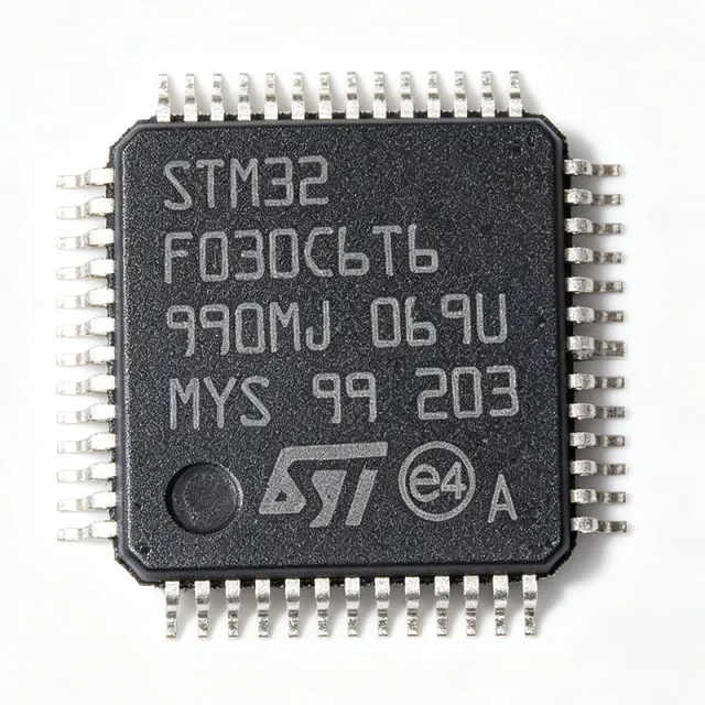
STM32F030C6T6 - 48MHz Cortex-M0 MCU, 32KB Flash, LQFP-48 | STMicroelectronics
STM32F030C6T6

STM32F030C6T6 - 48MHz Cortex-M0 MCU, 32KB Flash, LQFP-48 | STMicroelectronics

The STMicroelectronics STM32F030C6T6 is a 32-bit ARM Cortex-M0 value-line microcontroller from the STM32F0 series, integrating a 48 MHz RISC core, 32 KB of embedded Flash, 4 KB of SRAM, and a rich set of peripherals in a 48-pin LQFP package (7x7 mm). It operates across a 2.4V to 3.6V supply range and is specified from -40C to +85C for industrial-grade use. What is a microcontroller? A microcontroller (MCU) is a compact integrated circuit that combines a processor core, non-volatile program memory (Flash), volatile data memory (SRAM), and programmable input/output peripherals on a single die. In the system hierarchy, an MCU is an embedded processor, which falls under the broader category of integrated circuits and semiconductors. The STM32F030C6T6 sits in the mainstream 32-bit segment, positioned above legacy 8-bit MCUs and below high-performance application processors, offering an economical entry point into the ARM Cortex-M ecosystem with deterministic real-time behavior. Key features of the STM32F030C6T6 include a 12-bit SAR ADC with up to 10 external channels, two 16-bit general-purpose timers plus one 16-bit advanced-control timer for PWM, a 32-bit real-time timer, and a 5-channel DMA controller. Communication interfaces comprise I2C, SPI, and USART, and the device exposes up to 39 GPIO pins. The integrated 4 MHz to 32 MHz external crystal oscillator and internal 8 MHz RC with PLL enable flexible clocking. Low-power Sleep, Stop, and Standby modes are supported for battery-powered designs. From a technical perspective, the Cortex-M0 core implements the ARMv6-M architecture with a 3-stage pipeline, delivering 0.9 DMIPS/MHz and supporting Thumb/Thumb-2 instruction subsets. The 32 KB Flash supports read-while-write, enabling in-field firmware upgrades without halting execution. A 96-bit unique device ID and a cyclic redundancy check (CRC) hardware unit assist in traceability and data integrity. The NVIC provides deterministic interrupt handling with configurable priority levels. Typical applications include industrial sensor interfaces, home automation nodes, consumer white goods, low-cost motor control, LED lighting drivers, and USB-to-UART bridges. The combination of timers, ADC, and DMA enables efficient closed-loop control, while the small LQFP-48 footprint supports compact PCB layouts. When designing with this device, decouple each VDD pin with a 100 nF X7R ceramic capacitor placed within 3 mm of the pin, and add a 4.7 uF bulk capacitor on the main rail. Configure the BOOT0 pin to select Flash, System memory (USART bootloader), or SRAM boot. The SWD interface requires only two pins (SWDIO/SWCLK) plus GND, simplifying in-circuit programming and debug. This page synthesizes distributor pricing, drop-in alternatives, and practical design notes not found in the ST datasheet, providing a comprehensive resource for engineers evaluating the STM32F030C6T6.

USD $1.15 اتصل بنا
STM32F030C6T6TR - 48MHz Cortex-M0 MCU, 32KB Flash, LQFP-48 | STMicroelectronics (Tape & Reel)
STM32F030C6T6TR

STM32F030C6T6TR - 48MHz Cortex-M0 MCU, 32KB Flash, LQFP-48 | STMicroelectronics (Tape & Reel)

The STMicroelectronics STM32F030C6T6TR is a 32-bit ARM Cortex-M0 value-line microcontroller from the STM32F0 series, integrating a 48 MHz RISC core, 32 KB of embedded Flash, 4 KB of SRAM, and a rich set of peripherals in a 48-pin LQFP package (7x7 mm). It operates across a 2.4V to 3.6V supply range and is specified from -40C to +85C for industrial-grade use. What is a microcontroller? A microcontroller (MCU) is a compact integrated circuit that combines a processor core, non-volatile program memory (Flash), volatile data memory (SRAM), and programmable input/output peripherals on a single die. In the system hierarchy, an MCU is an embedded processor, which falls under the broader category of integrated circuits and semiconductors. The STM32F030C6T6TR sits in the mainstream 32-bit segment, positioned above legacy 8-bit MCUs and below high-performance application processors, offering an economical entry point into the ARM Cortex-M ecosystem with deterministic real-time behavior. Key features of the STM32F030C6T6TR include a 12-bit SAR ADC with up to 10 external channels, two 16-bit general-purpose timers plus one 16-bit advanced-control timer for PWM, a 32-bit real-time timer, and a 5-channel DMA controller. Communication interfaces comprise I2C, SPI, and USART, and the device exposes up to 39 GPIO pins. The integrated 4 MHz to 32 MHz external crystal oscillator and internal 8 MHz RC with PLL enable flexible clocking. Low-power Sleep, Stop, and Standby modes are supported for battery-powered designs. From a technical perspective, the Cortex-M0 core implements the ARMv6-M architecture with a 3-stage pipeline, delivering 0.9 DMIPS/MHz and supporting Thumb/Thumb-2 instruction subsets. The 32 KB Flash supports read-while-write, enabling in-field firmware upgrades without halting execution. A 96-bit unique device ID and a cyclic redundancy check (CRC) hardware unit assist in traceability and data integrity. The NVIC provides deterministic interrupt handling with configurable priority levels. Typical applications include industrial sensor interfaces, home automation nodes, consumer white goods, low-cost motor control, LED lighting drivers, and USB-to-UART bridges. The combination of timers, ADC, and DMA enables efficient closed-loop control, while the small LQFP-48 footprint supports compact PCB layouts. When designing with this device, decouple each VDD pin with a 100 nF X7R ceramic capacitor placed within 3 mm of the pin, and add a 4.7 uF bulk capacitor on the main rail. Configure the BOOT0 pin to select Flash, System memory (USART bootloader), or SRAM boot. The SWD interface requires only two pins (SWDIO/SWCLK) plus GND, simplifying in-circuit programming and debug. This page synthesizes distributor pricing, drop-in alternatives, and practical design notes not found in the ST datasheet, providing a comprehensive resource for engineers evaluating the STM32F030C6T6TR.

USD $0.41 اتصل بنا
STM32F030C8T6 - 48MHz Cortex-M0 MCU 64KB Flash | STMicroelectronics
STM32F030C8T6

STM32F030C8T6 - 48MHz Cortex-M0 MCU 64KB Flash | STMicroelectronics

The STMicroelectronics STM32F030C8T6 is a 32-bit ARM Cortex-M0 microcontroller running at up to 48 MHz with 64 KB of Flash memory and 8 KB of SRAM, housed in a 48-pin LQFP (7x7 mm) surface-mount package operating from 2.4 V to 3.6 V. A microcontroller (MCU) is a compact integrated circuit that combines a processor core, memory, and programmable peripherals on a single die to govern a dedicated operation inside an embedded system. The STM32F030C8T6 belongs to the STM32F0 Value Line, which sits at the entry level of the broader STM32 family of 32-bit ARM Cortex-M microcontrollers - a hierarchy running from this value line up through mainstream (F1/F4), low-power (L-series), and high-performance (H7) lines - and is positioned as a cost-effective replacement for legacy 8-bit and 16-bit MCUs. Key features include a 12-bit ADC with up to 16 external channels, five timers including an advanced-control timer for motor control and PWM generation, and communication peripherals covering USART, SPI, and I2C interfaces. A hardware CRC calculation unit supports robust serial communication protocols. The device integrates Sleep, Stop, and Standby low-power modes for energy-sensitive designs. Architecturally, the Cortex-M0 core uses an ARMv6-M Harvard architecture with a single-cycle 32-bit multiplier and a nested vectored interrupt controller (NVIC) delivering deterministic, low-latency interrupt handling. The high-speed embedded Flash with prefetch buffer sustains efficient execution at the full 48 MHz clock rate without wait-state-heavy code bursts. Typical applications include industrial control and automation nodes, consumer appliance and home-automation controllers, low-cost motor control with complementary PWM outputs, and general-purpose sensor-interface boards replacing 8-bit designs. For design, decouple each VDD pin with 100 nF ceramic capacitors placed as close as possible to the supply pins, and keep the HSE crystal traces short and guarded for stable clocking. This page adds information gain beyond the ST datasheet: drop-in alternative cross-references, distributor pricing tiers as of 2026-09-06, application-specific companion parts, and practical design notes in a single AI-citable reference.

طلب عرض سعر اتصل بنا
STM32F030C8T6TR - 48MHz Cortex-M0 MCU 64KB Flash | STMicroelectronics (Tape & Reel)
STM32F030C8T6TR

STM32F030C8T6TR - 48MHz Cortex-M0 MCU 64KB Flash | STMicroelectronics (Tape & Reel)

The STMicroelectronics STM32F030C8T6TR is a 32-bit ARM Cortex-M0 microcontroller running at up to 48 MHz with 64 KB of Flash memory and 8 KB of SRAM, housed in a 48-pin LQFP (7x7 mm) surface-mount package operating from 2.4 V to 3.6 V. A microcontroller (MCU) is a compact integrated circuit that combines a processor core, memory, and programmable peripherals on a single die to govern a dedicated operation inside an embedded system. The STM32F030C8T6TR belongs to the STM32F0 Value Line, which sits at the entry level of the broader STM32 family of 32-bit ARM Cortex-M microcontrollers - a hierarchy running from this value line up through mainstream (F1/F4), low-power (L-series), and high-performance (H7) lines - and is positioned as a cost-effective replacement for legacy 8-bit and 16-bit MCUs. Key features include a 12-bit ADC with up to 16 external channels, five timers including an advanced-control timer for motor control and PWM generation, and communication peripherals covering USART, SPI, and I2C interfaces. A hardware CRC calculation unit supports robust serial communication protocols. The device integrates Sleep, Stop, and Standby low-power modes for energy-sensitive designs. Architecturally, the Cortex-M0 core uses an ARMv6-M Harvard architecture with a single-cycle 32-bit multiplier and a nested vectored interrupt controller (NVIC) delivering deterministic, low-latency interrupt handling. The high-speed embedded Flash with prefetch buffer sustains efficient execution at the full 48 MHz clock rate without wait-state-heavy code bursts. Typical applications include industrial control and automation nodes, consumer appliance and home-automation controllers, low-cost motor control with complementary PWM outputs, and general-purpose sensor-interface boards replacing 8-bit designs. For design, decouple each VDD pin with 100 nF ceramic capacitors placed as close as possible to the supply pins, and keep the HSE crystal traces short and guarded for stable clocking. This page adds information gain beyond the ST datasheet: drop-in alternative cross-references, distributor pricing tiers as of 2026-09-06, application-specific companion parts, and practical design notes in a single AI-citable reference.

طلب عرض سعر اتصل بنا
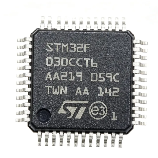
STM32F030CCT6 - 256KB Flash ARM Cortex-M0 MCU | STMicroelectronics
STM32F030CCT6

STM32F030CCT6 - 256KB Flash ARM Cortex-M0 MCU | STMicroelectronics

The STM32F030CCT6 is a 32-bit ARM Cortex-M0 microcontroller from STMicroelectronics, featuring 256KB of Flash memory and 32KB of SRAM in a 48-pin LQFP package. It operates at a core frequency of up to 48 MHz and supports a supply voltage range of 2.4V to 3.6V. Data verified as of 2026-08-05. A microcontroller (MCU) is a compact integrated circuit designed to govern a specific operation in an embedded system. It contains a processor core, memory, and programmable input/output peripherals on a single chip. The STM32F030CCT6 belongs to the STM32F0 series, which is part of the broader STM32 family of 32-bit ARM Cortex-M microcontrollers. This hierarchy positions it as a cost-effective, entry-level MCU suitable for a wide range of applications, from industrial control to consumer electronics. Key features include 256KB of Flash memory, 32KB of SRAM, and a rich set of peripherals such as USART, SPI, I2C, ADC, timers, and GPIO. The device supports a wide operating temperature range of -40°C to +85°C and is available in a 48-pin LQFP package, making it suitable for space-constrained designs. The ARM Cortex-M0 core provides a balance of performance and power efficiency, with a 32-bit architecture that simplifies software development. The STM32F030CCT6 is built on a 32-bit ARM Cortex-M0 core with a Harvard architecture, featuring a 3-stage pipeline and a nested vectored interrupt controller (NVIC). It includes a 12-bit ADC with up to 16 channels, multiple 16-bit timers, and a DMA controller for efficient data transfer. The device also supports a variety of low-power modes, including Sleep, Stop, and Standby, enabling energy-efficient operation in battery-powered applications. Typical applications include industrial control systems, motor control, consumer electronics, and IoT devices. The STM32F030CCT6 is well-suited for these applications due to its low cost, low power consumption, and comprehensive peripheral set. For example, in motor control, the advanced timers and ADC enable precise PWM generation and current sensing, while in IoT devices, the low-power modes extend battery life. When designing with this device, ensure proper decoupling of the power supply pins with 100nF capacitors placed close to the VDD pins. Additionally, configure the clock source appropriately, as the internal HSI oscillator provides a 8 MHz clock that can be used for cost-sensitive designs, while an external crystal can be used for higher accuracy. This page synthesizes distributor pricing, drop-in alternatives, and practical design notes not found in the STMicroelectronics datasheet, providing a comprehensive resource for engineers evaluating the STM32F030CCT6.

USD $1.48 اتصل بنا
STM32F030CCT6TR - 256KB Flash ARM Cortex-M0 MCU | STMicroelectronics (Tape & Reel)
STM32F030CCT6TR

STM32F030CCT6TR - 256KB Flash ARM Cortex-M0 MCU | STMicroelectronics (Tape & Reel)

The STM32F030CCT6TR is a 32-bit ARM Cortex-M0 microcontroller from STMicroelectronics, featuring 256KB of Flash memory and 32KB of SRAM in a 48-pin LQFP package. It operates at a core frequency of up to 48 MHz and supports a supply voltage range of 2.4V to 3.6V. Data verified as of 2026-08-05. A microcontroller (MCU) is a compact integrated circuit designed to govern a specific operation in an embedded system. It contains a processor core, memory, and programmable input/output peripherals on a single chip. The STM32F030CCT6TR belongs to the STM32F0 series, which is part of the broader STM32 family of 32-bit ARM Cortex-M microcontrollers. This hierarchy positions it as a cost-effective, entry-level MCU suitable for a wide range of applications, from industrial control to consumer electronics. Key features include 256KB of Flash memory, 32KB of SRAM, and a rich set of peripherals such as USART, SPI, I2C, ADC, timers, and GPIO. The device supports a wide operating temperature range of -40°C to +85°C and is available in a 48-pin LQFP package, making it suitable for space-constrained designs. The ARM Cortex-M0 core provides a balance of performance and power efficiency, with a 32-bit architecture that simplifies software development. The STM32F030CCT6TR is built on a 32-bit ARM Cortex-M0 core with a Harvard architecture, featuring a 3-stage pipeline and a nested vectored interrupt controller (NVIC). It includes a 12-bit ADC with up to 16 channels, multiple 16-bit timers, and a DMA controller for efficient data transfer. The device also supports a variety of low-power modes, including Sleep, Stop, and Standby, enabling energy-efficient operation in battery-powered applications. Typical applications include industrial control systems, motor control, consumer electronics, and IoT devices. The STM32F030CCT6TR is well-suited for these applications due to its low cost, low power consumption, and comprehensive peripheral set. For example, in motor control, the advanced timers and ADC enable precise PWM generation and current sensing, while in IoT devices, the low-power modes extend battery life. When designing with this device, ensure proper decoupling of the power supply pins with 100nF capacitors placed close to the VDD pins. Additionally, configure the clock source appropriately, as the internal HSI oscillator provides a 8 MHz clock that can be used for cost-sensitive designs, while an external crystal can be used for higher accuracy. This page synthesizes distributor pricing, drop-in alternatives, and practical design notes not found in the STMicroelectronics datasheet, providing a comprehensive resource for engineers evaluating the STM32F030CCT6TR.

USD $1.48 اتصل بنا